
Abstract
The diverse properties of two-dimensional materials have been utilized in a variety of architecture to fabricate high quality electronic circuit elements. Here we demonstrate a generic method to control hysteresis and stable memory effect in Van der Waals hybrids with a floating gate as the base layer. The floating gate can be charged with a global back gate-voltage, which it can retain in a stable manner. Such devices can provide a very high, leakage-free effective gate-voltage on the field-effect transistors due to effective capacitance amplification, which also leads to reduced input power requirements on electronic devices. The capacitance amplification factor of ∼10 can be further enhanced by increasing the area of the floating gate. We have exploited this method to achieve highly durable memory action multiple genre of ultra-thin 2D channels, including graphene, MoS2, and topological insulators at room temperature.
Export citation and abstract BibTeX RIS

Original content from this work may be used under the terms of the Creative Commons Attribution 4.0 licence. Any further distribution of this work must maintain attribution to the author(s) and the title of the work, journal citation and DOI.
The exfoliation of graphene, which provided the platform for the subsequent discoveries of several other atomically thin two-dimensional (2D) materials such as MoS2, hBN, and Bi-based topological insulators (TIs) have led to a revolution in the research of devices [1–11]. The weak interlayer van der Waals coupling allows these materials to be exfoliated even down to a single atomic layer, displaying several novel phenomenon. Some of the remarkable properties displayed by the Dirac Fermionic carriers in graphene and topological insulators (TIs) include room temperature quantum Hall effect, superconductivity, and quantum anomalous Hall effect [4, 12–18]. MoS2 is one of the most important members of the transition metal-dichalcogenide family, and has found numerous applications in electronics, optoelectronics, piezoelectricity, and valleytronics [7, 19–23]. The diverse properties of these materials have been best exploited by fabricating hybrids out of them, by stacking one on top of the other, leading to state-of-the-art sensors, and providing a solid platform for further miniaturization of devices and faster electronics [8, 9, 16, 18, 19, 24–42].
One major area of thrust with Van der Waals hybrids has been to achieve non-volatile, durable memory action, which provide several advantages such as reduced power consumption, higher integration density, and enhanced life-times [43, 44]. In this work, we have demonstrated a generic device architecture to achieve non-volatile memory effect in stacks made using 2D materials in a floating gate geometry [45–48]. While the floating gate geometry has been exploited in case of transition metal dichalcogenide-based in 2D atomic/molecular layers, it's applicability for a broader range of 2D materials, and an optimization of the architecture itself, remains unexplored. The floating gate can be charged by the application of a back-gate voltage (VG). The charge remains stored even after the gate-voltage is switched off due to lower back transfer probability, and gives rise to higher effective gate-voltage compared to that of the standard 285 nm SiO2. The cyclic charge trapping due to VG-dependent band-bending leads to a large hysteresis window, which can be accurately tuned by controlling the area of the floating gate. This effect can be utilized in a variety of devices such as extremely robust low power, non-volatile memory applications using MoS2, which is difficult to achieve with graphene due to the absence of any band-gap. The high effective VG can also be implemented to achieve ambipolar transport in topological insulators, and highly repeatable large hysteresis window, even at room temperature. Attaining ambipolar transport usually requires a large gate-voltage, and low temperature due to high residual bulk doping. Such devices can be utilized for exploring several properties of Dirac Fermions in TIs when access to the surface states is required.
The durable memory action in our devices is made possible due to the presence of the floating gate. Floating gate MOSFETs (FGMOS) have been extensively used as in memory applications such as EPROMs (Erasable Programmable Read Only Memories) and EEPROMSs (Electrically Erasable Programmable Read Only Memories), and can be used in neural networks as well [46, 49, 50]. With substantial improvement of the fabrication techniques and the emergence of two-dimensional materials, such circuits can be implemented using entirely Van der Waals materials, leading to further miniaturization. The advantage of using a floating gate rests in the amplification of the equivalent capacitance (Ceqv), and hence the effective VG on the channel, which is our case, is graphene, MoS2, and TIs. A typical schematic to understand the capacitance amplification in the present scenario is illustrated in figure 1(a) . Let C1 be the capacitance between the graphene channel and the 2DM underlayer. The thickness of this capacitor is equal to the thickness of hBN (dhBN), which also acts as the tunnel barrier in these devices. The area of the capacitor is equal to the area (A) of the channel. Let C2 be the capacitance between the Si back gate and the 2DM underlayer, whose thickness is equal to the thickness of SiO2 (dS) , and the area is equal to the area of the underlayer (A2D) . Let us now assume that the area of the underlayer is equal to the area of the channel (A2DM = A), which is illustrated in figure 1(a). Since C1 and C2 both have the same area and the dielectric constant of hBN and SiO2 are also similar ( r ∼ 4), we can write
  , where n = dS/dhBN. If VG is applied on the Si gate, and V0 is the voltage at the underlayer, since the charge induced on the underlayer and the channel is same, we can write


Figure 1. Basics of capacitance amplification: (a) The top panels show the capacitance circuits for devices without and with extended underlayers, respectively. C1 and C2 are underlayer to channel and underlayer to back gate capacitances (with area equal to the area of the channel), respectively. xC2 is the capacitance between the extended part of the the underlayer and the back gate. (b) The bottom panels show typical device schematics without and with the extended underlayer.
Download figure:
Standard image High-resolution imageIn real devices, however, the area of the underlayer is always larger, and can be expressed as A2D = A + xA. Here A is the part of the underlayer that is lying underneath the channel, and xA is the extended part of the underlayer located outside the channel area. In such a scenario, the capacitance between the Si gate and the underlayer ( ) can be expressed as
  , which is schematically represented in figure 1(b). This implies that the voltage at the underlayer VA can be expressed as,
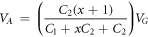
The capacitance amplification (AV) in our devices is defined as the ratio of VA and V0. It can be expressed as

Using the relation  and considering the fact that both
  , equation (3) can be rewritten as

Equation (4) clearly enunciates that the effective VG can be further enhanced by the increasing the area of the underlayer, a property which has been exploited in our present work.
The devices studied in this manuscript have been fabricated from several two dimensional materials such as single layer graphene (SLG), molybdenum disulphide (MoS2), Bi-based chalcogenide Bi1.6Sb0.4Te2Se topological insulators (TIs), and boron nitride. While the top channel is formed by graphene, MoS2, and TIs, the floating gate is primarily made of single or multi-layer graphene, and MoS2. In certain devices, the area of the floating gate has been extended by depositing 20 nm Au, which is connected only to the 2D underlayer only. In all our devices, hBN forms the tunnel barrier between the channel and the floating gate. In order to process these devices, graphene, MoS2, Bi1.6Sb0.4Te2Se, and hBN were separately exfoliated on standard 285 nm SiO2/Si substrate, followed by the fabrication of the required hetero-structure in a home-made transfer assembly. The contacts were patterned by standard electron beam lithography followed by thermal evaporation of 5/50 nm Cr/Au for source, and drain electrodes. All resistivity measurements were performed using a lock-in amplifier with a carrier frequency of 227 Hz, in a home-made variable temperature cryostat.
The preliminary transfer characteristics of a typical device using the floating gate geometry with single layer graphene as the top channel (figure 2(a)) is shown in figure 2(b), which exhibits two distinct features. Firstly, the transport in the graphene channel with 2DM underlayer displays a strong hysteresis between the forward and backward VG sweeps, while the standard hysteresis-free R vs VG is restored when the 2D underlayer is absent. Secondly, the sharpness of the transfer characteristics is significantly enhanced in the presence of the 2D layer, suggesting an increase in either the carrier mobility in the channel or the effective capacitance. Since hBN is the common substrate to the entire channel, both effects can only be due to the presence of the 2D underlayer. Both these effects, however, are absent when the 2D underlayer is electrically grounded, and the transfer characteristics is determined by the extent of VG-dependent screening by the doped 2D layer (see supplementary section A available online at stacks.iop.org/MRX/7/014004/mmedia). The extent of (anti-)hysteresis can be reduced, and eventually completely removed, by decreasing the sweep range below a critical value VCG (±12 V for the device in figure 2(c)), which suggests that the total trapped charge in the 2DM layer remains fixed as long as the sweep range is below VCG around the Dirac point. The enhanced sharpness of the transfer characteristics in the presence of the 2DM underlayer, however, has negligible effect on the range of the VG sweep.

Figure 2. Features of graphene-FETs with a floating gate: (a) Illustration of a typical graphene/hBN/MoS2 heterostructure along with the measurement circuit used. (b) The red and the green traces are the R − VG characteristics of graphene channel without and with the underlayer. The arrows indicate the sweep directions. (c) Traces of different colors present the R − VG transfer characteristics of the graphene channel having underlayer for different VG sweep range. The hysteresis vanishes for sufficiently small VG window (Green trace). (d) The measured and expected carrier density a function of VG with and without underlayer is presented as the red data points and the solid yellow line, respectively. (e) Tunability of the charge neutrality of the channel is demonstrated by hysteresis free R − VG and n − VG characteristics. (f) Schematics at the left presents the mechanism of voltage amplifications. The schematics in the top right and the bottom right panels shows the band diagram when the channel is highly doped with positive and negative charge, respectively.
Download figure:
Standard image High-resolution imageTo understand it's origin, we have extracted the carrier density n in the channel directly from Hall measurements. The measured n for forward and backward sweeps over a sweep range of 60 V is shown in figure 2(d). The dependence of n on VG is also (anti-)hysteretic, with the Dirac points coinciding with the reversal in the sign of the carriers. Around the Dirac points n varies linearly with VG, and the total capacitance (CG ) sis obtained from the slope. Evidently, CG is considerably larger than C0 (slope of the solid line in figure 2(d)), where  is the sum of the respective geometric capacitances of SiO2, 2DM and hBN layers in series. Here
  , and
, and  where dBN and
  are the thicknesses of the hBN and SiO2 layers, respectively. C2DM is usually 10–100 times larger that CBN and
  , and can be neglected. This confirms that the sharpness in the R − VG characteristics is indeed is due to enhanced CG, rather than an improbable increase in the carrier mobility in the channel region just above the 2DM underlayer. By restricting the sweep range below VCG, the variation of n with VG can be made completely non- hysteretic, irrespective of the location of the Dirac point, i.e. the extent of trapped charge in the 2DM underlayer. Figure 2(e) illustrates this at three locations of the Dirac point.
The clockwise hysteresis (i.e. anti-hysteresis) of R − VG in figure 2(f) is the effect of cyclic charge trapping by the 2DM due to VG-dependent bending of the hBN bands, and has been recently observed in memory devices based on trilayer Van der Waals hybrid of similar architecture [45, 47]. When VG increases in positive or negative directions from the Dirac point, the transfer of electrons or holes from the graphene channel to the 2DM causes an effective gate voltage shift, that can be erased only by reversing the polarity of VG. The enhancement in VA is limited by the band gap ΔBN of hBN, and for voltage  , electric field-induced band bending within hBN will cause charge to flow across the dielectric, thereby pinning the Fermi level of the channel. This allows us to estimate both
  , as well as the saturation carrier density nmax ∼ ε0εBNΔBN/edBN, both of which could be directly verified from their dependence on dBN. Further amplification of the effective capacitance can be achieved by enhancing the area of the floating gate, which can be done by connecting the underlayer with Au. Using this, AV has been found to increase by an order of magnitude (See Supplementary section B).
One of the shortcomings of graphene is the lack of a band-gap, rendering it unsuitable for non-volatile memory based applications. To circumvent this, we have utilized the floating gate technique in an MoS2 FET to evince the possibility of high performance and power efficient non-volatile memory devices. The device structure is shown in (figure 3(a)) where the graphene and molybdenum disulphide layer have been interchanged from (figure 2(a)). Similar hysteresis is also observed when MoS2 forms the top current carrying layer as demonstrated in figure 3(b) due to the screening of back gate electric field by the trapped charges in the floating gate. Such structures have been previously investigated in [45, 47, 51]. One of the major parameters that determine electronic device performances is the sub-threshold swing. It is defined as the amount of gate voltage bias required to change the source-drain current (Isd) by one decade, and is given by the following expression,

Here S is the surface potential in the channel. The second term in the equation (5) has Boltzman theoretical limit of 60 mV/decade at room temperature while the first term, known as the body factor is given by

where CS is the quantum capacitance of the channel. The equivalent capacitance for our extended floating gate structure is the capacitance of the hBN dielectric, which is much larger than that of the 285 nm SiO2. From equation (6) it is clear that higher the equivalent capacitance, lower is the value of sub-threshold swing (S) leading to faster switching, and reduced power consumption. The higher capacitance per unit area of hBN allows us to reduce the body factor significantly leading to almost ideal subthreshold slope in all the measured devices for over four decades of Isd as shown in the inset of figure 3(b).

Figure 3. Features of MoS2-FETs with a floating gate: (a) Graphical illustration of a typical MoS2 device. The bottom panel shows a hybrid after transfer, while the right image shows an optical micrograph of an actual device. (b) Hysteresis observed in MoS2 devices. Inset shows calculation of sub-threshold swing (S = 80 mV/decade for the representative device). (c) Temporal dependence of drain current after a program (−9/−7 V) or erase (+9/−7 V) pulse for a drain bias of 10 mV (yellow line) and 50 mV (blue line). (d) Demonstration of the repeatability of memory action for over 100 cycles of program and erase pulse. The memory ratio, defined as the ratio of the on and off state current, for 100 cycles is shown in the inset.
Download figure:
Standard image High-resolution imageThe large memory window and the near ideal subthreshold swing (figure 3(b)) make the extended floating gate MoS2 devices perfect candidates for non-volatile memory storage. The binary memory action is depicted in figure 3(c) with a ON/OFF ratio of ≈ 103 at a drain bias of 50 mV, with a pulse time of 1 section. The pulse rise time has a significant effect on the on/off ratio, which is expected due to increased storage of charges on the floating gate, and is depicted for pulse widths of 0.1, 1, and 10 msec (Supplementary section C.1). The devices also show excellent retentivity, with negligible change of ISD upto ∼10000 secs for all three pulse times (Supplementary section C.1). To obtain the switching transition, a program and erase pulse of +9 and −9 V respectively was applied to the silicon back gate. The memory action is robust and repeatability has been checked for 100 program and erase cycles (figure 3(d)). We find a very low cycle to cycle variability in the memory ratio, defined as the ratio of the on and off state current, demonstrating the reliability of these non-volatile memory devices (inset of figure 3(d)). Furthermore, the memory ratio in our devices, which can be as high as 108, is comparable to state of the art sensors fabricated with two-dimensional materials, that have reported in literature (Supplementary section C.2) [52–59]. Additionally, the low bias requirements and program state current value makes the device power efficient with an observed power dissipation of ≈10 pW in the program state in our MoS2 based memory devices [51]. A lower stress on the gate dielectric due to reduced program and magnitude improves the reliability of these devices making them ideal for low power portable memory applications.
We have further exploited this technique by using topological insulators (TIs) as the conducting channel. High bulk conductivity due to doping from defects in the bulk makes it difficult to tune the Fermi level across the Dirac point, and achieve ambipolar transport. This severely limits the T range for practical applications of TIs since the surface transport regime remains inaccessible. This problem can be circumnavigated either by going to very low temperatures, where the bulk doping is suppressed, which is not a feasible solution for several practical applications, or by using an ionic liquid top gate, can degrade the device characteristics due to intercalation of ions [60–65]. To address this, we have utilized capacitance amplification to access the Dirac Fermion dominated transport regime, even at high T. To fabricate the devices, the TI Bi1.6Sb0.4Te2Se was used, which offers reduced bulk number density due to compensation doping, and the transport below T < 50 K for samples with thickness d < 100 nm is primarily through the surface [66–68]. The scanning electron micrograph of a typical device with MoS2 as the floating gate is shown in figure 4(a). The R − VG as shown in figure 4(b) shows ambipolar transport at T = 22 K, and remarkably at T = 300 K as well. Similar transfer characteristics were observed in devices with multi-layer graphene as the floating gate (Supplementary section D.1). Such large and controlled hysteresis in TI-FETs clearly demonstrate that they can be used in non-volatile memory operations at room temperature. The percentage change in R, however, is ∼10%–20%, which implies that only the bottom surface is affected by the VG, and the top surface remains unaffected due to screening of VG by the bottom surface and the bulk. The measured R is possibly limited by the top surface, and any residual bulk conducting channels. To verify the ambipolar nature of transport, we have performed Hall measurements in the sample at different VG-s across the Dirac point. The Hall number density (n), extracted using  , is shown in Figure 4(c), as a function of VG, where RH is the Hall co-efficient. The number density shows a clear change in sign across the Dirac point, thus validating the ambipolar nature of transport in our TI devices. The capacitance of the stack can be estimated using ne = Ceqv(VG − VD), and is equal to 7.5 × 10⁻⁴ F, which is ∼6 times larger than the 285 nm SiO2 dielectric. The R-VG data for several sweep rates clearly indicates that the hysteresis is independent of the sweep rate (Supplementary section D.2). From R − VG at different temperatures, the impurity density as well as mobility of the TIs can be extracted from T = 22–300 K (Supplementary section D.3). The mobility of the sample increases as the T is reduced, as expected. However, the value of mobility is low (< 50 cm2V−1S−1) at low T, even though the samples are on BN. This is in stark contrast to a medium like graphene, since μ increases manifold when the SiO2 substrate is replaced by the atomically flat BN, where the effect of trapping-detrapping and dangling bonds on the electrical transport in the sample is significantly reduced. This clearly signifies that the low mobility in TI samples can be attributed to the contribution of bulk defects which act as the dominant scattering centers [68–71], and provide an intrinsic limit to the mobility.

Figure 4. Features of TI-FETs with a floating gate: (a) Scanning electron micrograph of a typical TI-FET with MoS2 as the floating gate. (b) Resistance vs gate-voltage behavior at T = 22 K and 300 K, both exhibiting ambipolar transport. (c) Number density, extracted from Hall measurements vs VG, displaying a change in sign across the Dirac point, thus verifying the ambipolar nature of the transport.
Download figure:
Standard image High-resolution image
In summary, we have utilized capacitance amplification due to a floating gate in Van der Waals hybrids fabricated out of graphene, MoS2, and topological insulators. The increase in effective capacitance leads to an increase in the effective gate-voltage on the conducting channel, which shows a large hysteresis due to cyclic trapping and detrapping of charges. This effect has been used in a variety of ultra-thin materials like graphene, MoS2, and topological insulators to demonstrate highly stable, non-volatile memory response at room temperature. Our work provides a framework for employing hybrids of atomically thin quantum materials for memory-based applications requiring high durability, and low power .
Acknowledgments
The authors thank the Department of Science and Technology, Government of India for funding. The authors thank CenSe, IISc for nanofabrication facilites.