
Abstract
Van der Waals epitaxy enables the integration of 2D transition metal dichalcogenides with other layered materials to form heterostructures with atomically sharp interfaces. However, the ability to fully utilize and understand these materials using surface science techniques such as angle resolved photoemission spectroscopy (ARPES) and scanning tunneling microscopy (STM) requires low defect, large area, epitaxial coverage with ultra-clean interfaces. We have developed a chemical vapor deposition van der Waals epitaxy growth process where the metal and chalcogen sources are separated such that growth times can be extended significantly to yield high coverage while minimizing surface contamination. We demonstrate the growth of high quality 2D WS2 over large areas on graphene. The as-grown vertical heterostructures are exceptionally clean as demonstrated by ARPES, STM and spatially resolved photoluminescence mapping. With these correlated techniques we are able to relate defect density to electronic band structure and, ultimately, optical properties. We find that our synthetic approach provides ultra-clean, low defect density (~1012 cm−2), ~10 μm large WS2 monolayer crystals, with an electronic band structure and valence band effective masses that perfectly match the theoretical prediction for pristine WS2.
Export citation and abstract BibTeX RIS
Interest in transition metal dichalcogenides (TMDs), such as WS2, MoS2 and related compounds, has been renewed by the discovery of emergent properties when reduced to single, two-dimensional (2D) layers [1, 2]. These atomically thin layers of TMDs form a versatile and vast library of 2D materials [3]. On the one hand, they are useful for studying novel condensed matter phenomena, such as strong excitonic many-body interactions or topological phases [4–6], while on the other, they hold great promise for applications in electronics, optoelectronics, and catalysis [7–10]. A defining characteristic of 2D materials is that the interaction with the substrate or, more generally, with any interfacial layer plays a critical role in their electronic and optical properties due to the reduced electrostatic screening in two dimensions [11, 12].
In this context, other layered materials, such as graphene or hexagonal boron nitride (h-BN), can serve as advantageous substrates for synthesis of 2D TMDs via van der Waals epitaxy. For layered materials, the weak van der Waals interaction between individual layers allows the growth of unstrained 2D films that are crystallographically aligned to the underlying substrate even in the presence of a large lattice mismatch [13–20]. Graphene provides a conductive support that is ideal for vertically integrated electronic devices and electronic spectroscopy such as scanning tunneling spectroscopy or photoelectron spectroscopy [21]. The main challenge to understand and use these vertical heterostructures is that the growth process of the TMD induces such a high level of surface contamination and defect density that the resulting optical and electronic properties are strongly impacted by the locally varying defects [22].
In terms of gas phase synthesis, however, the use of layered van der Waals materials as substrates poses certain challenges. Due to the absence of dangling bonds at the growth substrate interface, reactants from the gas phase adsorb via weak van der Waals interactions only, and the growth occurs in a regime where the lateral growth rate is slow, which in turn leads to small crystal domains [14, 23]. For 2D TMDs, metal oxide powder chemical vapor deposition (CVD) is one of the most common approaches to synthesize 2D materials due to its simplicity, versatility, and low cost [24–26]. Several studies have already established the feasibility of directly growing 2D TMDs on van der Waals substrates, in particular graphene and h-BN, via CVD [16, 18, 27]. However, in a conventional reaction geometry, the metal oxide precursor is exhausted before the growth is complete due to the chalcogenation reaction of the oxide precursor, as recently demonstrated for wafer-scale CVD of MoS2 on sapphire [25]. Consequently, the slow lateral growth rate of TMDs on van der Waals substrates mostly results in isolated submicrometer grains with low surface coverage, which limits the applicability of powder CVD to wafer-scale van der Waals epitaxy on these substrates [16, 27, 28]. The common use of solid sulfur or selenium as chalcogen sources adds additional complexity in controlling the amount of precursor during gas phase reaction, which in turn has a significant impact on the reproducibility of the growth process [29]. Direct CVD of TMDs on van der Waals substrates would therefore benefit from a process that uses a well controlled, non-exhaustive precursor supply.
Here, we use a modified, atmospheric pressure CVD system where the metal and chalcogen precursors are separated such that the growth time could be extended significantly to yield large area growth. We use H2S as a precise chalcogen source which provides enhanced control over the growth conditions [30, 31]. This process was applied to synthesize monolayer WS2 on SiC/graphene substrates via van der Waals epitaxy. Monolayer islands up to 10 micron lateral size were grown, with homogeneous distribution and coverage up to 25% across the substrates. Using surface sensitive techniques such as atomic resolution scanning probe microscopy (STM) and angle resolved photoemission spectroscopy (ARPES), for in-depth characterization of these heterostructures, we find that the as-synthesized monolayers are exceptionally clean and can readily be characterized, even after exposure to atmospheric conditions. Moreover, we demonstrate nanoscale ARPES with spatial resolution down to 230 nm, which opens up the possibility to explore the fundamental electronic structure of nanoscale or heterogeneous 2D systems, such as lateral 2D heterostructures. Our synthetic scheme based on gaseous chalcogen precursors instead of chalcogen powders combined with a nearly unlimited metal oxide supply offers a straightforward extension to controlled growth of TMD heterostructures.
Results and discussion
Figure 1(a) depicts the modified CVD reactor used for the van der Waals growth of 2D TMDs. The horizontal tube furnace system consists of an outer 1 inch quartz tube and an inner 1/4 inch quartz tube, the latter terminating at the center of the hot zone. The tubes are equipped with separate gas supply lines. The inner tube is connected to an Argon supply line, whereas the outer tube is connected to Argon and H2S supply lines. The metal oxide precursors are loaded into the inner tube and the growth substrate is placed directly next to its outlet. Unlike the standard approach, where the metal oxide powder is supplied in an open crucible or boat, the depicted configuration slows down the chalcogenation of the metal oxide [25]. Therefore, the growth time can be extended to achieve large domain sizes even on van der Waals materials such as h-BN or graphene where the lateral growth rate is low. The growth procedure is detailed in the methods section.
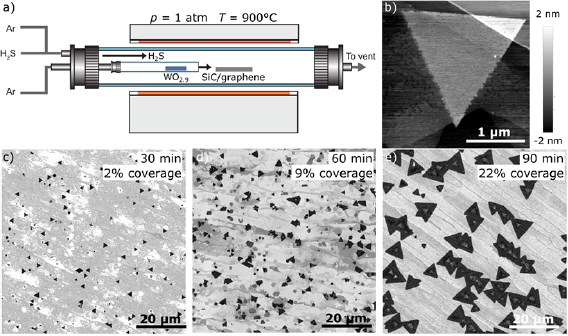
Figure 1. Ambient pressure chemical vapor deposition. (a) Modified tube furnace system with separate gas supplies for outer and inner tube. Tungsten oxide powder (WO2.9) loaded in the inner tube serves as the metal source. Hydrogen disulfide (H2S) and Argon (Ar) serve as chalcogen source and carrier gas, respectively. The SiC/graphene substrate is placed next to the outlet of the inner tube at the center of the hot zone. Due to the separation of metal and chalcogen precursor flow, the growth time can be extended without exhausting the precursors, which results in increased domain size and surface coverage. (b) Atomic force microscopy image of monolayer WS2 domain on epitaxial graphene. (c)−(e) Electron microscope images of CVD-grown WS2 islands where increased growth time leads to increased surface coverage and domain size. The WS2 islands appear as dark contrast.
Download figure:
Standard image High-resolution imageFigures 1(c)–(e) depict representative scanning electron microscope (SEM) images of WS2 islands grown with the modified CVD system. In SEM, the WS2 domains appear as dark contrast. The substrate consists of stepped, atomically flat terraces of mono- and bi-layer graphene (figure 1(b)) prepared by ambient pressure graphitization of SiC(0 0 0 1) [32]. For the shortest growth time of 30 min, we find strictly triangular monolayer WS2 domains. Statistical analysis of the SEM images yields a surface area coverage of 2.5%. Similar to recent reports, the orientations of the monolayer domains are registered to the substrate [16, 28, 33]. Upon increasing the growth time from 30 min to 60 min, we observe an apparent increase of the average domain size and a significant increase of the surface area coverage to 9%. In figure 1(e), the growth took place for 90 min and the average domain size approaches 10 microns at a surface area coverage of 25%. We note that for this particular substrate, the SEM images and Raman mapping (figure S1) (stacks.iop.org/TDM/5/045010/mmedia) clearly indicate multilayer regions at the center of WS2 domains which are located at the step edges of the SiC/graphene substrate. Since it is known that such step edges can act as nucleation sites for growth of 2D materials [34], we conclude that these multilayer regions are nucleation sites. This is consistent with the observed homogeneous size distribution in the images, from which we infer that in figure 1(e) the initial nucleation step occurred at the same time for a majority of the crystallites. We speculate that this particular nucleation behavior may be ascribed to the increased average step height of about 5 nm for the substrate in figure 1(e) compared to 1 nm for the substrates in figures 1(c) and (d). These larger step edges provide very effective nucleation sites and lead to the formation of crystal domains with multilayer centers and monolayer edges. The difference in step height is due to the slightly different miscut angles of the wafers. The step height was determined by AFM (not shown). We confirmed the increase of surface coverage and domain size with increasing growth time on several sets of substrates. Importantly, we achieve 50% film coverage in selected areas, where the growth conditions are apparently improved due to, for example, optimum precursor supply conditions (figure S2). This suggests that further increasing the growth time can lead to continuous film growth. We find that the domain shape sometimes deviates from strictly triangular, which indicates a regime in-between chalcogen- and metal-rich conditions and suggests a certain variability in the metal oxide precursor flow [24]. Although the modified tube furnace geometry effectively slows down the chalcogenation of the oxide precursor by establishing a laminar flow of pure Ar in the metal precursor line, back-diffusion of Ar/H2S still leads to partial chalcogenation of the metal oxide for extended growth times. As demonstrated recently [25, 35], the reproducibility of the metal oxide precursor supply can be greatly enhanced for such a furnace geometry by a small amount of additional oxygen flow in the metal oxide precursor line. Enhanced control over the metal precursor supply may also aid in deliberately controlling the initial nucleation step, which depends critically on the concentration of the precursor available on the surface.
We used room temperature photoluminescence (PL) spectroscopy to characterize the optical properties of the as-grown films. Figure 2(a) shows a spatial map of the integrated PL emission intensity of a WS2 monolayer island. For CVD-grown TMDs, often spatially inhomogeneous patterns of exciton emission are reported, such as bright edge regions or dark intragrain boundaries, which is usually attributed to local changes in strain or chemical composition due to variations during the growth process [30, 36–38]. Our optical characterization reveals two main insights. First, these samples maintain a strong photoluminescence intensity despite sitting directly on graphene. Second, we find that within the spatial resolution of 300 nm, the emission intensity is uniform and we observe no brightening or darkening of the exciton emission related to morphological features, such as the edges or intragrain boundaries. The spectral mean of the exciton emission yields further information on the local optical properties (figure 2(b)). We find distinct spatial fluctuations of the exciton emission energy on the order of 10 meV whereby the lateral size of the fluctuations is given by the instrument resolution. Similar to the emission intensity, the spectral shape of the emission is not correlated to the morphology of the WS2 monolayer or the underlying substrate.

Figure 2. Photoluminescence spectroscopy of WS2 monolayers on epitaxial graphene. (a) Integrated PL intensity map of a WS2 monolayer domain on graphene. (b) Spectral mean of the WS2 emission spectrum. (c) PL spectra of WS2 at edge position (black curve, rightward triangle) and center position (blue curve, leftward triangle). The inset shows a histogram of the spectral mean of the WS2 domain depicted in (b).
Download figure:
Standard image High-resolution imageImportantly, the spatial homogeneity with graphene as a substrate is increased compared to TMD monolayers grown on non-epitaxial substrates such as SiO2, where the spectral fluctuations are reported to be on the order of 25 meV to 50 meV [12, 30, 38]. Figure 2(c) depicts representative PL spectra measured at the center and the edge of the triangular domain. The spectra exhibited are merely shifted by approximately 10 meV and have the same, symmetric peak shape with a FWHM of 40 meV indicating mostly excitonic emission. The reminiscent spatial heterogeneity may be attributed to random fluctuations in the density of point defects in the WS2 (as discussed later for the STM analysis) or to heterogeneity in the substrate such as charge puddling in the graphene layers, which is expected to be reduced even further by using h-BN as the growth substrate [39]. However, the observed fluctuations are very small compared to conventionally grown samples, and combined with the exciton dominated emission indicate high optical quality of these WS2 flakes. We also characterized the optical quality of the larger domains (figure S1) that result from increasing the growth time to 90 min (see figure 1(e)) by Raman and PL imaging, and we observed a comparable spatial homogeneity of the excitonic properties. To further corroborate the quality of our materials we investigated their electronic band structure.
The electronic band structure of the WS2 films were determined by angle resolved photoemission spectroscopy (ARPES). ARPES also has the advantage of being supremely sensitive to the surface, reflecting any adsorptive or defect related modification of the electronic structure. Figure 3 shows ARPES intensity maps of a single WS2 monolayer domain. The experiments were conducted using the nano-ARPES endstation at the MAESTRO beamline of the Advanced Light Source. The data was acquired at a photon energy of 95.4 eV and at in-plane momenta of 1.2 Å−1 <  < 3.8 Å−1, which is outside of the first Brillouin zone. Figure 3(a) depicts a spatial photoemission map of the integrated valence band intensity at Γ2 near
  = 2.2 Å−1, which clearly resolves a triangular WS2 monolayer domain, with a spatial resolution of 230 nm full width at half maximum (FWHM), in line with the selected measurement geometry. The measurement geometry was selected to allow a signal-to-noise ratio sufficient to resolve the band structure from an area as small as 300 nm × 300 nm (figure S4). The analyzer was oriented such that the measured trajectory in k-space intersects a Γ-point and a K-point outside of the first Brillouin zone (inset of figure 3(b)). At these large in-plane momenta the APRES intensity is enhanced compared to the first Brillouin zone, and contributions from the graphene substrate are minimized (figure S3). Consequently, we can precisely resolve the structure of the spin–orbit split valence bands around the K-point (figure 3(c)). We determine the spin–orbit splitting at K to be ΔSO = (425 ± 5) meV, and the distance between the valence band maxima at Γ and K to be ΔEKΓ = (240 ± 3) meV. These results are in excellent agreement with theoretical predictions [40] and recent experiments on single layer WS2 on h-BN/TiO2, where the TMD is decoupled from the conductive TiO2 substrate [41]. However, our values differ significantly from previously reported ones for WS2 on graphene/SiC, which are 462 meV for the spin–orbit splitting and 182 meV for the distance of the valence bands between Γ and K [21]. The discrepancy between these results may be attributed to the different positions of the valence band maxima, equivalent to a different doping, with respect to the Fermi level, which are −1.84 eV for [21] and −1.13 eV for this work. The intrinsic charge density in turn determines the effect of manybody renormalization effects on the band structure measured by ARPES [41, 42].
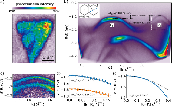
Figure 3. Band structure of a single triangular domain of monolayer WS2 on epitaxial graphene. (a) Spatial photoemission intensity map of the integrated intensity of the valence band near the Γ-point of WS2. The spatial resolution is set and checked to be 230 nm (FWHM). (b) Averaged ARPES intensity map of the monolayer WS2 domain shown in (a). The spectrum was measured outside of the 1st Brillouin zone (see inset). (c) ARPES intensity map near the K-point (dashed rectangle in (b)). (d) Dispersion of the two topmost valence bands at the K-point. A parabolic fit of the dispersion in the region near the maximum (solid black line) yields effective masses of meff = (0.41 ± 0.01) me and meff = (0.52 ± 0.04) me. For large values of |k − K|, the dispersions begin to deviate from the parabolic model (grey dashed line). (e) Dispersion of the topmost valence band at the Γ-point with effective mass meff = (2.33 ± 0.1) me.
Download figure:
Standard image High-resolution imageFigure 3(d) depicts the dispersion of the valence band near K obtained by fitting the ARPES spectra with Gaussian line profiles (figure S5). Using a parabolic model for the dispersion, we extract hole effective masses of (0.41 ± 0.01) me for the upper valence band and (0.52 ± 0.04) me for the spin–orbit split valence band. Our results match previously reported values while greatly improving on the precision in those measurements due to the high spatial resolution of the MAESTRO beamline, enabling the measurement of a single WS2 domain [21, 43]. We note that the apparent value of the effective mass is sensitive to the choice of the fitting range due to the trigonal warping term, which becomes significant at large values of |k − K|. Therefore, we determined the effective mass from a region very close to the K point (|k − K| < 0.06 Å−1). For the effective mass at the Γ point we find meff = (2.33 ± 0.1) me within a range |k − Γ| < 0.1 Å−1 (figure 3(e)). In all cases, the value of the effective mass is sensitive to the choice of the fitting range around the high symmetry points and accounts for most of the quoted uncertainty value. Table 1 compares our results to experimentally and theoretically determined band parameters for WS2 from the literature. The agreement of our experimental results with theoretical predictions for freestanding, pristine WS2 and experimental results on WS2 decoupled from the substrate indicate that our synthetic process can provide high quality TMD materials that exhibit electronic properties on par with theoretical predictions and close to those of intrinsic monolayer WS2. To get the ultimate insight into the effective structure we synthesized, we employed low temperature non-contact atomic force microscopy/scanning tunneling microscopy (nc-AFM/STM) to study the quality of our material with atomic resolution.
Table 1. Experimental and theoretical valence band parameters of monolayer WS2. At the K point, the effective masses of the upper valence band and lower valence band are quoted in the upper and lower row, respectively. ΔSO is the spin–orbit splitting between the valence bands at K and ΔEKΓ is the distance between the valence band maxima at K and Γ.
| Reference | meff at K (me) | meff at Γ (me) | ΔSO at K (meV) | ΔEKΓ | Substrate |
|---|---|---|---|---|---|
| This work (experiment) | (0.41 ± 0.01) | (2.33 ± 0.1) | (425 ± 5) | (240 ± 5) | SiC/graphene |
| (0.52 ± 0.04) | |||||
| Ref. [51] (experiment) | (0.45 ± 0.05) | (1.55 ± 0.13) | 420 | 260 | TiO2 |
| (0.63 ± 0.17) | |||||
| Ref. [21] (experiment) | 0.39 | (462 ± 5) | 182 | SiC/graphene | |
| 0.53 | |||||
| Ref. [43] (experiment) | (0.40 ± 0.02) | (419 ± 5) | 510 | Au(1 1 1) | |
| (0.57 ± 0.09) | |||||
| Ref. [40] (theory) | 0.35 | 2.18 | 429 | 252 | Vacuum |
| 0.49 |
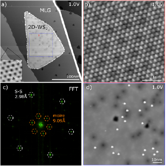
The epitaxial graphene on SiC constitutes an atomically-flat, electronically homogeneous substrate that is almost ideal for STM of 2D materials [19, 33]. Figure 4(a) shows a representative large area scan of a WS2 monolayer island. For all samples we find that, except for the edges, the TMD islands are ultra-clean and free from adsorbates after mild annealing at ~300 °C for 30 min in ultrahigh vacuum. Consequently, atomic resolution could be routinely achieved on both graphene and WS2 (figure 4(b)). The lattice mismatch between WS2 and graphene gives rise to a characteristic moiré pattern and the atomic registry of the WS2 lattice was usually rotated only by a few degrees with respect to the graphene lattice (figure 4(c)) [44]. Using scanning tunneling spectroscopy at T ≈ 5 K, we measured an electronic band gap of monolayer WS2 on monolayer graphene of 2.47 eV. A smaller band gap of 2.35 eV was found on bilayer graphene, owing to the increased screening by the substrate [42]. Figure 4(d) depicts an STM image where individual point defects can clearly be discerned, appearing as bright and dark spots under the given imaging conditions. It is worth noting that throughout all samples the point defects appear randomly distributed across the islands without any prevalence towards the domain edges or the center. This is consistent with the PL characterization which did not show any systematic correlation of optical properties and morphology. In turn, these findings corroborate that the presented synthesis method yields crystalline domains which are structurally and chemically homogeneous due to the improved control of the metal oxide precursor. From larger-scale STM images, we derived a cumulative defect density of 1011–1012 cm−2, depending on the sample. Note that the necessary annealing process for UHV STM is known to induce chalcogen vacancies as defects [45]. While the determined defect density is already low, the as synthesized defect density is considerably lower than our measurement, explaining the excellent optical properties and band structure. Detailed electronic characteristics of these defects are not within the scope of the manuscript and they will be discussed elsewhere. Line defects within single islands such as mirror twin boundaries, as reported for other TMD materials and growth methods, were not observed, suggesting that the domains grow as single crystals from single nucleation events [4, 19].
Figure 4. Scanning tunneling microscopy. (a) STM topography (I = 50 pA, V = 1 V) of a single monolayer WS2 island on epitaxial graphene. The inset at the bottom left (I = 20 pA, V = 0.2 V) shows the atomically resolved graphene honeycomb lattice. (b) Atomic resolution STM image of the area indicated by the small red rectangle in (a) showing the WS2 lattice and the moiré pattern with the underlying graphene substrate. (c) 2D Fourier transform of the image in (b) with the peaks corresponding to the hexagonal sulfur sublattice and the moiré pattern. (d) STM image of WS2 at the location indicated by the blue dashed rectangle in (a). The bright and dark features correspond to single point defects in the WS2 layer.
Download figure:
Standard image High-resolution image
Conclusion
In summary, we have synthesized and extensively characterized vertical WS2/graphene heterostructures via a modified metal oxide powder CVD-process. Contrary to the most commonly applied CVD process which uses solid metal and chalcogen precursors [19, 21, 33, 46], we employed a hybrid approach which uses a solid metal precursor (tungsten oxide powder) and a gaseous chalcogen precursor (H2S). Furthermore, the modified geometry of the reactor separates the metal oxide precursor from the chalcogen, such that chalcogenation of the metal precursor over time is prevented and the growth time can be extended to yield higher monolayer coverage. While the use of H2S as sulphur source has been demonstrated before for CVD of monolayer MoS2 and solid state sulfurization of few-layer MoS2 and WS2 [30, 31, 47, 48], the presented methodology constitutes a further improved handle on both the metal and chalcogen precursor supply. We analyzed the pristine 2D WS2 structures with a combination of highly surface sensitive techniques, STM and ARPES, with minimal further processing. Importantly, we demonstrate nanoscale electronic band structure measurements by nano-ARPES, and they indicate that the WS2 is largely decoupled from the graphene substrate. At the K point, we calculate the effective masses of the valence bands to be (0.41 ± 0.01) me for the upper valence band and (0.52 ± 0.04) me for the lower valence band, and for the spin–orbit splitting we find (425 ± 5) meV, fitting excellently to theoretical band structure calculations for pristine WS2. In STM, we find that the dominant defects are randomly distributed point defects and we estimate their upper limit of defect density to be 1011–1012 cm−2. Overall the material quality, as assessed by STM and ARPES, compares favorably with studies on TMD monolayers grown by metalorganic chemical vapor deposition, which generally provides superior control and reproducibility [49, 50]. Yet, metal oxide powder based CVD still offers the benefit of extreme ease and versatility [26], and our hybrid CVD approach, that uses gaseous chalcogen precursors and improved control over the metal oxide source, will therefore be applicable not only to the specific case of WS2 but the van der Waals epitaxy of most TMDs.
Methods
Epitaxial graphene growth
Graphene was synthesized on nominally on-axis 6H–SiC(0 0 0 1) following the procedure described in [32]. Before graphene epitaxy, the substrates were etched in hydrogen (atmospheric pressure, T = 1650 °C, t =15 min) yielding atomically flat, stepped surfaces with typical step width of 1 μm–10 μm and step height of 1 nm–5 nm depending on the specific wafer. Graphene growth was carried out under Argon flow (T = 1700 °C, t = 15 min). This procedure yields 1–3 layers of graphene.
Tube furnace/growth conditions
We used a modified CVD tube furnace system, which consists of an outer 1 inch tube and an inner 1/4 inch tube, whereby the latter terminates at the center of the hot zone. The tubes have separate gas supplies (outer tube: Ar and H2S, inner tube: Ar). About 10 mg WO2.9 powder (Alfa Aesar, 99.99% (metals basis)) were loaded into the inner tube and the growth substrates were placed directly next to the outlet. Both the substrate and the tungsten oxide precursor were located in the constant temperature region of the hot zone. Before loading, the substrates were sonicated in ethanol and blow dried with nitrogen. Pure argon (Praxair Ultra High Purity Grade, 99.999%) passed through an oxygen/moisture trap (Agilent OT3-4) served as a carrier gas. We used pure H2S (Praxair, 99.6%) as the chalcogen source. After loading the samples, the tube furnace was pumped to low vacuum (~10 torr) and purged with dry Ar multiple times before restoring to atmospheric pressure under Ar flow (outer tube: 20 sccm, inner tube: 4 sccm). The center temperature of the furnace was increased from room temperature to the growth temperature T = 900 °C over 15 min and held at that temperature for 30 min to 90 min in total. 4 sccm H2S were added to the gas flow of the outer tube when the desired growth temperature was reached. At the end of the growth period, heating was switched off, and the Ar flow in the inner tube was set to zero to terminate the metal oxide precursor supply. The H2S flow was maintained during cooldown to prevent the formation of chalcogen vacancies. Once the temperature in the hot zone fell below 500 °C, the furnace was purged with dry Argon gas (outer tube: 500 sccm) and H2S was switched off. The process took place at atmospheric pressure.
Morphological and optical characterization
The synthesized structures were characterized by atomic force microscopy (Park NX-10, tapping mode), electron microscopy (Zeiss Ultra-55, E = 1 keV–10 keV) as well as combined Raman and photoluminescence spectroscopy (WITEC Alpha 300R, λexcitation = 532 nm, room temperature, ambient conditions).
Scanning tunneling microscopy
The experiments were performed using a CreaTec low-temperature (T ≈ 5 K), ultra-high vacuum (p ≈ 10−10 mbar) STM. The voltage was applied to the sample. STM images were taken in constant-current mode. A CO-functionalized tip was created by picking up a single CO molecule from a Au(1 1 1) surface.
Angle resolved photoemission spectroscopy
Angle resolved photoemission intensity maps were recorded using a Scienta R4000 analyzer on a selected WS2 domain using a focused photon beam at the MAESTRO beamline at the advanced light source (ALS). The photon energy was set to 95.4 eV and the sample held at room temperature. The base pressure during the measurements was below 10−11 mbar.
Acknowledgments
Work at the Molecular Foundry was supported by the Office of Science, Office of Basic Energy Sciences, of the US Department of Energy under Contract No. DE-AC02-05CH11231. This research used resources of the Advanced Light Source, which is a DOE Office of Science User Facility under contract no. DE-AC02-05CH11231. B Schuler appreciates support from the Swiss National Science Foundation under project number P2SKP2_171770.