
Abstract
The growth of two-dimensional layered chalcogenides on two- or three-dimensional substrates, named (quasi) van der Waals epitaxy, has been pioneered by the group of A. Koma at Tokyo University in 1985. The passive nature of the van der Waals surface is important in energy converting interfaces as solar cells and photoelectrochemical cells. For those reasons the two-dimensional materials have intensively been studied by us in the early 90s of the last century. The growth of different 2D/2D, 2D/3D and 3D/2D heterostructures has been studied with an emphasis on the electronic structure of the materials and their interfaces, which have been characterized using photoelectron spectroscopy and are reviewed in this contribution. Our work includes a discussion of the coupling of electronic states across the interfaces, which influences the growth behavior and determines energy band alignment. The weak electronic coupling allowed the first experimental determination of the band structure of a single layer of a 2D chalcogenide, namely WS2. We also review the electronic structure of a GaSe half-sheet terminated Si(111) surface, which provides an ideal platform for the integration of 2D materials with Si microelectronics.
Export citation and abstract BibTeX RIS

This is an open access article distributed under the terms of the Creative Commons Attribution Non-Commercial No Derivatives 4.0 License (CC BY-NC-ND, http://creativecommons.org/licenses/by-nc-nd/4.0/), which permits non-commercial reuse, distribution, and reproduction in any medium, provided the original work is not changed in any way and is properly cited. For permission for commercial reuse, please email: permissions@ioppublishing.org.
Layered Materials and Their Applications
Layered chalcogenides are considered to be prototypes of two-dimensional inorganic materials. Their basic structural, electronic and physical properties have thoroughly been investigated, which is documented in a number of original papers and books.1–5 The crystal structures of the layered chalcogenides of formal stoichiometry MX2 and M2X2 (M = metal, X = chalcogen) are shown in Fig. 1.

Figure 1. Crystallographic structure of different layered chalogenides. Reprinted by permission from Springer Nature Customer Service Center GmbH from Ref. 6, Copyright (2000).
Download figure:
Standard image High-resolution imageThey are characterized by two-dimensional sandwich units of X-M-X or X-M-M-X atomic layers (the sandwiches form a close-packed structure). Along the crystallographic c-direction the sandwich units are separated from each other by the so-called van der Waals-gap. Close-packed and chemically saturated chalcogenide atoms form the inner surfaces. The bonding within the sandwich units is strong and is based on covalent bonds with some electrostatic contribution depending on the ionicity of the M–X bonds. The metals are found in a trigonal prismatic coordination for more covalent chalcogenides to optimize the covalent overlap, whereas more ionic compounds prefer octahedral coordination minimizing the electrostatic repulsion.7 A special case are the chalcogenides of In and Ga with the formal stoichiometry MX (M2X2), which contain metal-metal single bonds of group III elements. The bonding of the sandwich units to each other is weak along the crystallographic c-axis and is often referred to as van der Waals-like. However, as is already evident from the band dispersion calculated and measured along the c-direction (normal) to the van der Waals plane there is a non-negligible electronic interaction across the van der Waals gap (see discussion below). An electronic coupling of adsorbates interacting with the van der Waals surface have also been deduced e.g. from H2O induced upward Fermi level shifts indicating electron donation into the layered transition metal chalcogenides (see e.g. Refs. 8 and 9).
A prominent application of layered materials is lubrication,10,11 utilizing the low adhesive forces between the van der Waals-planes. In contrast to other lubricants, the layered materials are solid and stable up to high temperatures and therefore can be used in vacuum and space environments. Layered materials are also applied as catalysts for the hydrodesulfurization reaction,12 with transition metals used as promotors. The reversible intercalation of lithium allows the application as battery electrodes,13,14 although presently oxide electrodes are favored because their larger voltages. Layered materials have also been studied for solar cell applications, as ideal interface properties are expected without recombination losses.15–19
Nanotubes of WS2 and MoS2 have already been fabricated in early years11,20,21 and those of GaSe were investigated theoretically.22 Additionally, the layered chalcogenides have been intensively investigated as photoelectrochemical cells (see Refs. 8, 15, and 23, and contribution of B. Parkinson.24), but high performance could only be reached if defects in the bandgap, which may occur on edge planes or at defects on the van der Waals plane, will not play an active role. Recently MoS2 has been discovered as effective H2 evolution catalyst:25–28 For this application defects on the van der Waals plane are needed to be efficient. Evidently, the observed physical and chemical properties may be very different depending on the preparation of the 2D layered materials and must be studied in detail to understand the origin of the observed performance. Therefore, it must be checked, which of the many interesting results found in recent years using 2D chalcogenides are intrinsic properties of ideal van der Waals heterointerfaces or whether defects formed during the synthesis of the 2D chalcogenides or during the processing of the heterostructures may play a decisive role. Most of the recent studies on van der Waals hetero structures use exfoliation and coupling techniques or CVD based synthesis procedure for their manufacturing.25,29–34 In these cases, the quality (defect absence or defect origin) of the van der Waals surfaces and their cleanliness (there is a strong tendency of CH-adsorbate sticking) are very often not checked properly, for example using sub-monolayer sensitive surface science studies. Just from measurements of the optical and electric properties of the prepared device structures this severe problem can hardly been clarified. For a detailed mechanistic understanding it is necessary to relate the observed properties of 2D quantum size structures to studies on model systems which have been prepared in UHV combined with a detailed analysis of the surface and interface properties. Therefore, we have summarized in this review our past results on the electronic properties of surfaces and interfaces of layered chalcogenides prepared using van der Waals-epitaxy in ultrahigh vacuum (UHV), to provide benchmarks for perfect van der Waals heterointerfaces.
2D van der Waals Type Heterostructures in Materials Science
A number of interesting new physical and chemical phenomena are related to the miniaturisation of materials approching nano-sized dimensions. The controlled manufactoring and processing of materials in the extreme case on the atomic and monolayer level has developed to an important and strongly emerging field of materials science which will allow to pave the way to advanced device structures especially in optical, electronic, optoelectronic, thermal, catalytic, sensing, and electrochemical applications, A decisive factor is the dimensionality of the nano-structures ranging from OD to 3D systems. Specifically the 2D layered materials, which are the focus of these issues of the ECS, have been intensively investigated in recent years following the groundbreaking results of Novoselov and Geim on graphene,35,36 which have been awarded with the nobel prize in 2010. Afterwards the scientific efforts investigating the fundamental properties but also possible applications of extremely thin 2D layered materials have strongly been increased covering all aspects of materials science, physics, and chemistry. Starting from synthesis and manufacturing, a detailed chemical and physical characterization on the nanoscale is provided, which is followed by processing issues involving functionalization, manipulation, metrology, and finally the applications of 2D materials in many technology fields (for some recent reviews on 2D van der Waals heterostructures see e.g. Refs. 25, 37–45).
Originally, the material of interest was mostly graphene and its specific properties and applications as single or ultrathin layer. However, because of the missing bandgap the variability is limited and other classical 2D materials, such as boron nitride, transition metal dichalcogenides (TMDs), transition metal carbides, nitrides, or carbonitrides (MXenes), oxides and emerging 2D materials such as borene, phosphorene, silicene, germanene, antimonene have been included in the studies. A schematic summary of the most interesting 2D materials under consideration is given, for example, in Refs. 37 and 45. With this set of materials there is a wide playground for a lego design box to new materials as the interfacial coupling is considered to occur via their van der Waals gaps, which are usually discussed in terms of a van der Waals type of interaction.45 Especially the layered metal chalcogenides provide a wide variety of physical properties. Depending on their structure and chemical composition metallic, semiconducting as well as insulating materials are available. Also the chemical interactions may be very different: there exist layer sequences with different transition metal ions between two chalcogenide layers with the sequence (X-T-X, see Fig. 1). There are also main group elements which form layered structures (e.g. in the sequence X-M-M-X as in InSe (see Fig. 1) or X-M-X-M-X e.g. as in Bi2S346) but also layered systems where both the metal and the chalcogenide is exposed to the van der Waals gap as in SnS.46 This wide variety of materials showing a layered structure indicates already that the term van der Waals interaction may be not correct for describing the interlayer interaction as will be discussed in more detail in this review.
Even before the renewed interest in 2D layered materials, layered chalcogenides have been studied intensively because of their ideal surface properties.1–3 As the ideal van der Waals surface exposing a close packed layer of chalcogenide atoms is chemically rather inert, very many interesting investigations on surface interactions without considering chemical bond formation have been performed in the past either under ambient conditions but also in electrochemical environment8,15,23,47 (see also the contribution of B. Parkinson in this focus issues24). Therefore, one may argue that the layered chalcogenides provide ideal boundary conditions for fundamental surface and interface studies outside vacuum conditions. However, because of their chemically saturated van der Waals-surfaces, they are also outstanding candidates for fundamental studies of interface properties in UHV. The most recent review of our work on the interface properties of layered heterointerfaces has been given by Jaegermann, Klein and Pettenkofer.6 Some previous contributions also consider adsorption and electrochemistry.15,23 The results presented therein will be shortly summarized to introduce the materials and results already obtained before. More recent results on the electronic properties of the surfaces, thin films and interfaces are described in more detail in this contribution. Although being an essential part of these investigations, this review does not include a detailed description of "van der Waals-epitaxy", which has been introduced by Koma's group back in 1985,48 as it is outside the length limit and scope of this work. The reader interested in the growth of the films used for the studies reported here is referred to our previous review6 and references therein, which gives an extensive survey of van der Waals epitaxy as performed in UHV environment.
Electronic Structure of Layered Chalcogenides
Transition metal dichalcogenides
The bulk electronic structure of layered transition metal dichalcogenides is described in Refs. 49–51. A detailed discussion of interlayer interactions will be given below). Electronic interactions across the van der Waals-gap, or across a heterointerface with a van der Waals-surface, are due to electronic states, which orbitals are directed perpendicular to the layers. These states will be referred to as z-states. In addition to the z-states there are pure x, y-statesa but also xz, yz-states according to different combinations of the chalcogen px and py states. In Fig. 2 the x, y-states are labelled as x+-states and the xz and yz-states as x−-states.b Within the P63/mmc space group, which is appropriate for the group VIb transition metal dichalcogenides (except WTe2), the x+-states have the same symmetry properties as the metal  and dxy-states and the x−-states have the same symmetry as the metal dxz and dyz-states (for more details see Ref. 52). The x+, x− and the corresponding z-states are symmetrized according to the irreducible representations of the space group. The symmetry labels identifying these irreducible representations at the center of the Brillouin zone Γ are also given in Fig. 2.
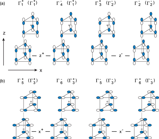
Figure 2. Combinations of chalcogen pz (a) and px, py-orbitals (b) according to the symmetry of layered chalcogenides in the 2H (or β) polytype. (Reprinted with permission from Ref. 52. Copyright (2001) by the American Physical Society.) The states can be divided into intralayer bonding and antibonding combinations (superscripts + and − at z or x). Both states can be subdivided into interlayer bonding and antibonding combinations. At the top of each orbital combination the symmetry label at the center of the Brillouin zone Γ is given. Labels in brackets are for single layer materials.
Download figure:
Standard image High-resolution imageMattheis49 and Coehoorn et al.51 give a detailed description of the electronic states of group VIb TMDCs close to the energy gap. As an illustration a band structure calculation for WS2 based on density functional theory using the scalar relativistic, self-consistent augmented sperical wave (ASW) method is shown in Fig. 3,52 together with the hexagonal Brillouin zone. Symmetry labels according to electronic states described in Fig. 2 are given for Γ and A. The valence band maximum  -state is located at the center of the Brillouin zone and is formed by metal
  and chalcogen pz-states51 (for more details see below). Unoccupied conduction band states at Γ are 2–3 eV above the valence band maximum and formed only by x+ and x−-states. The conduction band minimum is located on the line connecting Γ and the Brillouin zone boundary at K. Different metal and chalcogen orbitals contribute to this state. However, the contribution of z-states to the conduction band minimum is rather small.51

Figure 3. Brillouin zone and electronic band structure of WS2 calculated by using a self-consistent augmented spherical wave method. (Reprinted with permission from Ref. 52. Copyright (2001) by the American Physical Society).
Download figure:
Standard image High-resolution imageThere is considerable contribution of z-orbitals to conduction band states of layered Mo and W dichalcogenides for wave vectors off the hexagonal symmetry axis (k∥ > 0). This is because non-hybridized  and pz-states will disperse upwards in energy,49,53 when the parallel component of the wave vector k∥ is increased from zero.
A discussion of the contribution of z-states to the conduction band requires a more detailed consideration of the metal  and chalcogen pz-states. In Fig. 4 the occupied electronic states at Γ are given in the order of their binding energy. There are two pairs of
  and
and  -states, which have intralayer bonding character with respect to the chalcogen pz-orbitals. These orbital combinations have the same symmetry as the metal
  -states. As a consequence of identical symmetry, hybridization between pz and
  occurs at
  and
and  . The two pairs of states are different with respect to metal-chalcogen bonding. Bonding combination of pz and
  leads to the high binding energy
  and
and  -states. The valence band maximum is formed by a metal
  -chalcogen pz antibonding
  -state, which has been pointed out first by Coehoorn et al.51 Intralayer antibonding pz-states (
 and
and  ) do not hybridize with metal
  because of the missing horizontal mirror plane. Energetically they are situated approximately between the
  -pz bonding and antibonding combinations.
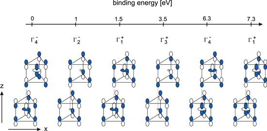
Figure 4. Occupied electronic valence states at Γ with contributions from metal  and chalcogen pz-states in the order of increasing binding energy. The
  and
and  -states are mixtures of chalcogen pz and metal
  with different signs of pz and
  in adjacent layers. The
  and
and  -states appear twice because of a different intralayer coupling of pz and
  .
.
Download figure:
Standard image High-resolution imageThe ionization energies of the chalcogen pz and the metal  -orbitalsc are different, leading to different contributions of metal and chalcogen orbitals to the two pairs of
  and
and  -states. The metal-chalcogen bonding combinations at higher binding energies have larger chalcogen p contributions, while the low binding energy states have larger metal d contributions.
As already mentioned above, the z-states should disperse upwards in energy when k∥ increases from zero.d This is not readily identified in the band structure (Fig. 3) since hybridization between z and x+ (and x−) states occurs for  , which leads to a forbidden crossing of energy bands. This hybrization between (mostly)
  and
and  -states is the origin of the energy gap in TMDCs.49 Nevertheless z-states have to be expected to contribute to the conduction band. As outlined in the preceeding paragraph, the contribution of chalcogen p-orbitals to the electronic states decreases with lower binding energy and the contribution of metal d-orbitals increases. Upward dispersing z-states should therefore reduce their chalcogen character. Thus, the contribution of z-states to the conduction bands should thus be mostly due to metal
  -states. This general argument is supported by detailed calculations of orbital contributions to the electronic states of MoSe2 given by Coehoorn et al.51 While metal
  -states contribute to the conduction band minimum and considerably to the slightly higher K5 conduction band state, no significant contributions of chalcogen pz-orbitals to the conduction band states are mentioned.
To summarize this section the contribution of z-orbitals to the electronic states of TMDCs close to the energy gap have been identified. At the center of the Brillouin zone all valence band states with binding energies 0–2 eV are derived from chalcogen pz and metal  -orbitals. Contributions of z-orbitals to conduction band states close to the energy gap exist only for k∥ > 0 and are mainly due to metal
  -orbitals.
InSe and GaSe
Although the van der Waals-surfaces of the III-VI-compounds InSe and GaSe are also formed by an hexagonal array of close-packed and chemically saturated selenium atoms as in the case of the TMDCs, their electronic structure is significantly different. This is due to the replacement of the transition metal atom by two group III metal atoms. A detailed description of the electronic structure of III-VI-compounds is given in the literature.55–57 More details will be discussed below. InSe is a direct gap semiconductor with valence band maximum and conduction band minimum located at Γ for the β (2H) polytype, or at Z for the γ (3R) polytype, respectively. The difference in electronic structures of the various polytypes is mainly explained by the different extension of the unit cell along c. The energy bands of the different polytypes can be mapped onto each other by suitable folding procedures. If this is done, almost identical electronic structures are found for the different polytypes.57
In the simplest description of the electronic structure of layered III-VI compounds the valence band maximum is derived from chalcogen pz-orbitals and the conduction band minimum from metal pz-orbitals (see also Fig. 27). However, as described for the TMDCs, hybridization between chalcogen and metal states is important. More detailed results for InSe are reported by Gomes da Costa et al.57 According to them, the valence band maximum is composed of 70% Se pz and 30% In pz-orbitals, while the conduction band minimum is composed of Se s (37.5%), Se pz (25%) and In s-orbitals (37.5%). Significant contributions of chalcogen z-states to both the valence band maximum and the conduction band minimum exist for the III-VI compounds InSe and GaSe. Both band extrema are found at k∥ = 0.
In summary, the bulk electronic band structure of 2D layered chalcogenides show a small but clearly existing dispersion of the electronic states in the direction perpendicular to the van der Waals surface, which is due to the electronic coupling of the different pz and  states (see Figs. 2–4). These electronic states are also involved to different degrees, depending on lattice mismatch, in the electronic hybridization across the van der Waals gap when heterostructures are formed.
Growth and Structure of Interfaces
2D/2D interfaces
The weak interaction across the van der Waals-gap is the conceptual basis for the growth of epitaxial layers of one type of layered compound on a layered chalcogenide substrate (2D/2D epitaxy, see Fig. 5). The interactions between two van der Waals-surfaces of different layered compounds is similar to the interlayer interactions in a layered crystal. As a consequence epitaxial films may be grown combining such van der Waals-compounds even when the lattice mismatch  is very large. The concept and term van der Waals-epitaxy (vdWe) have been introduced by Koma et al., who first studied the deposition of NbSe2 on the (0001) van der Waals-surface of MoSe2 single crystalline substrates.48 The prepared interfaces and their electronic properties have been summarized before.6

Figure 5. Interfaces of lattice mismatched materials as prepared by conventional (3D/3D) and van der Waals-epitaxy (2D/2D) (top). Low-energy electron diffraction of thin SnS2 layers grown on a MoS2 substrate (center). Scanning tunneling microscopy images of InSe layers on different layered substrates (bottom). Reprinted by permission from Springer Nature Customer Service Center GmbH from Ref. 6, Copyright (2000).
Download figure:
Standard image High-resolution imageThe growth and nucleation of van der Waals-epitaxy films has been studied with different techniques (see Ref. 6 and references therein). Two examples are shown in Fig. 5. Epitaxial growth and orientation of the overlayer is obvious from low-energy electron diffraction (LEED). The hexagonal diffraction pattern of the growing overlayer is superimposed and aligned to the substrate pattern for intermediate film thicknesses.58 Although the epitaxial relation is affected by the substrate only for very large lattice mismatch,6 the nucleation might be different as shown by the STM of InSe films deposited on GaSe, MoTe2 and highly oriented pyrolytic graphite (HOPG) (Fig. 5). These differences are clearly related to the different lattice constants; We attribute the different nucleation behavior to the different strength in the electronic coupling of the overlayer to the various substrates.6
The azimuthal orientation of the epitaxial layer to the substrate, which in van der Waals-epitaxy comes along without evidence for an in plane lattice relaxation, is a typical characteristic of the fundamental nature of its orientational interactions. The detailed analysis of the electronic structure of layered compounds proof that there is a small but non-negligible electronic overlap of the electronic states across the van der Waals-gap, which must depend on the orientational arrangement. In the layered chalcogenides the so-called van der Waals gap is formed between the chalcogen layers of two adjacent sandwiches. The chalcogen atoms of the top sandwich unit are situated in threefold hollow sites formed by the chalcogen atoms of the underlying sandwich. In this geometrical arrangement the chalcogen atoms form weak bonding interactions by the overlap of their pz orbitals with orbitals of the metal atoms of the underlying sandwich unit (see Fig. 4). Due to the lattice mismatch and the specific growth mode in van der Waals-epitaxy it is not possible for all chalcogen atoms to occupy threefold hollow sites. In contrast, some chalcogen atoms of the epilayer film must also sit ontop of substrate chalcogen atoms leading to height modulations. Ohuchi and Parkinson59,60 observed Moiré-like structures for MoSe2 on MoS2 using STM studies, which has been explained by such height undulations. Moiré patterns have also observed for few other material combinations61,62 and have been analyzed theoretically by Kobayashi.63,64 Tiefenbacher et al. also observed Moiré like pattern by LEED (Fig. 6) where the I-V analysis also favours a height undulation of the overlayer.65 The LEED-pattern associated with the undulation fades out after 2–3 layers and transforms to a standard hexagonal pattern as shown in Fig. 6 with increasing film thickness. Moiré-like LEED-patterns have also been observed for very slowly prepared ultra thin films of InSe deposited by MBE on TiSe2.66 A height undulation should in principle occur for all lattice mismatched vdWe-systems but has, unexpectedly, only been observed in a few substrate/-film combinations. The reason is not clear yet, but can most probably also be related to small differences in the electronic coupling across the vdWe-heterointerface (see also Refs. 63 and 64).

Figure 6. (top) LEED-pattern of a MoTe2 substrate (a) and of the growing WS2 film (b)–(d). A Moiré-like superstructure is observed for low coverages (b) and (c), which disappears with increasing film thickness (d). The sample has been tilted to monitor the (00)-spot; (bottom) schematic representation of the buckling of a single layer grown on a lattice mismatched substrate induced by the variation of interlayer z-state coupling (for more details and additional LEED-patterns see Ref. 65).
Download figure:
Standard image High-resolution image3D/2D interfaces
After the introduction of van der Waals-epitaxy it has been shown that epitaxial layers with large lattice mismatch can also be grown when layered chalcogenides are combined with three-dimensional materials. In Fig. 7 the typical 3D/2D material combinations of interest are schematically sketched. A precondition of such interface growth is in most cases the growth of an hexagonally arranged close packed layer of the 3D material on top of the hexagonally arranged substrate layer surface. For example fcc metals like Cu, Ag, and Au may form epitaxial (111) oriented films on layered chalcogenide (0001) surfaces (2D/3D; used convention: substrate/overlayer).67,68 Epitaxial layered chalcogenide films may also be grown on hexagonally close packed (111)-surfaces of cubic semiconductor substrates as Si(111):H or GaAs(111) (3D/2D).69,70 Oriented growth has also been observed for II-VI semiconductors on layered chalcogenide (0001)-surfaces,71 although strong clustering of the overlayer occurs. These type of heteroepitaxy was named quasi-van der Waals-epitaxy (qvdWe) as the heterointerface was formed between the van der Waals (0001)-surface of the layered compound and a surface plane of a non-layered material, e.g. the (111) plane of fcc compounds, which contains hexagonally close packed atoms.

Figure 7. Interfaces between three-dimensional and two-dimensional materials (quasi-van der Waals-epitaxy interfaces).
Download figure:
Standard image High-resolution imageAlready at the very beginning of quasi-van der Waals-epitaxy research it was considered to use this approach as buffer layer for conventional lattice mismatched semiconductors. Therefore, different 3D materials (metals as well as semiconductors) have been combined with 2D layered chalcogenides as substrates aiming at 3D/2D, 2D/3D and also 3D/2D/3D combinations (see Fig. 7). As first quasi-van der Waals-epitaxy interfaces, metal/semiconductor combinations were prepared and investigated (see Ref. 72 and references therein). For non-reactive interfaces, atomically abrupt metal/semiconductor interfaces are evidently formed.68,73–77 For noble metals such as e.g. Ag deposited on WSe2 (0001) the LEED-pattern shows a superposition of undisturbed substrate and overlayer diffraction spots of the Ag film with the 3-fold symmetry of the (111)-plane68 (see Fig. 8) As in the case of vdWe interfaces no evident lattice stress or strain is observed for the deposited film. The perfect orientation and high crystallinity of Ag (111) is also evident from the typical Shockley type surface state as identified by angle-resolved valence band spectroscopy.75 But, different to vdWe, island growth is usually obtained in qvdWe as for metal films, which is readily identified with STM measurements,78,79 but also for 3D semiconductor overlayer growth (see below).

Figure 8. LEED-pattern of silver islands grown on a WSe2 (0001) substrate.6,68 The outer hexagon corresponds to uncovered substrate regions while the inner three spots correspond to the silver islands. Reprinted by permission from Springer Nature Customer Service Center GmbH from Ref. 6, Copyright (2000).
Download figure:
Standard image High-resolution imageAlready in the last century, a lot of different quasi-van der Waals-epitaxy heterointerfaces have been prepared by numerous groups (for a summary see Ref. 6). Also 2D layered chalcogenides were deposited onto 3D substrates, which was also first demonstrated by Koma's group using a lattice mismatched (17%) hetero structure by deposition of MoSe2 on perfectly F-terminated CaF2(111).80 Also the growth of GaSe on GaAs substrates with different surface orientations have been reported,81–84 but the structure of the interface has not been identified.80 Ohuchi et al. proposed the formation of a GaSe interface layer on GaAs(111)81 whereas Tatsuyama et al. reported a layer-by-layer growth of GaSe on As or Ga terminated GaAs(111) surfaces.82,84 Interestingly, it also possible to grow (0001) oriented GaSe films on GaAs(100) surfaces despite the completely different surface symmetry82–84 assuming the formation of a Ga2Se3 interface layer. GaSe layers grow onto slightly misoriented GaAs(100) surfaces with a considerably inclined c-axis.85,86 As these examples indicate the qvdWe grown heterointerface GaSe/GaAs is not atomically sharp as originally assumed but may contain interface layers depending on the GaAs surface orientation, pretreatment and growth conditions. This is also observed for the growth of GaSe on Si(111) surfaces, which have been investigated in very detail (see below).
Before discussing this important heterostructure, we like to present some other interfaces applying 3D semiconductor growth onto layered chalcogenide (0001) surfaces. Such interfaces are a precondition for the manufacturing of technologically intriguing device structures using 2D buffer layers in lattice mismatched 3D systems. The first reports on 3D/2D/3D systems have been published by Palmer et al.87–89 showing GaAs growth on a thin GaSe buffer layer on As-terminated Si(111). The 3D GaAs grows as strongly clustered films with large azimuthally oriented islands of approx. 200 nm in diameter. The deposition of 2–6 compounds on layered substrates has also been demonstrated by Löher et al.71,90–92 On MoTe2 a (0001)-oriented film of CdS (Wurtzite structure) was deposited (mismatch 17%) (see Fig. 9). Similar results have been obtained for CdTe, ZnSe and CdS deposition on WSe2, MoTe2 and InSe (0001).71,91,92 The crystallites are all azimuthally oriented with respect to the substrate showing their intrinsic lattice constants. In most cases a strong clustering of the growing film is observed (see e.g. a typical STM images obtained for ZnSe/GaSe interfaces as shown Fig. 9).

Figure 9. (a) Low energy electron diffraction recorded during stepwise growth of CdS on MoTe2. Reprinted by permission from Springer Nature Customer Service Center GmbH from Ref. 6, Copyright (2000); (b)–(c): SEM images, (d) AFM image and (e) schematic arrangement of ZnSe nanoclusters on GaSe.93
Download figure:
Standard image High-resolution imageDue to the higher surface tension of the 2–6 compound overlayer relative to those of the van der Waals-surfaces of the layered chalcogenides a Vollmer-Weber growth mode is expected and also observed for most cases. Remarkable in this context is the growth of CdS on the layered compound InSe. Löher94 achieved oriented epitaxial growth even at room temperature and also initial layer-by-layer growth. But, the CdS film starts to roughen and forms facets of the S-terminated (111) surface toward vacuum for higher coverages. Therefore, additional experiments on the application of InSe buffer layers between Si and CdS or ZnSe have been performed, also showing crystalline orientation95,96 and photoactivity of the deposited ZnSe layer.97 In summary, the growth of highly crystalline qvdWe-heterointerfaces have already been proven for a number of combinations (2D/3D, 3D/2D, 3D/2D/3D). These studies allow to investigate the electronic properties of the formed layers and interfaces in very detail, as will be shown later in this contribution.
Van der Waals-epitaxy therefore offers the possibility to use layered materials as buffer layers in three-dimensional epitaxy between lattice mismatched materials (3D/2D/3D) but also for 2D quantum sized heterostructures. Because of the weak interactions across van der Waals surfaces, this should enable the growth of fully relaxed multilayers of different substrates making use of their intrinsic 2D electronic properties. Therefore, an in depth understanding of the electronic properties of van der Waals-epitaxy interfaces is required, which depends on the crystalline quality of the interface arrangement and the electronic coupling strength. With van der Waals-epitaxy it is, in principle, possible to combine electronically dissimilar materials under defined conditions. In combination with nanofabrication, which has also been shown already at the early times with layered materials using different STM and AFM techniques,98–107 a large variety of new devices and applications should be within reach. This is a main driver of the recent renewed interest in van der Waals type heterinterfaces. However, more extensive work is needed to optimize growth conditions in order to obtain heterodevices with well-defined interfaces. Therefore, the (q)vdWe 2D heterostructures provide reference data on interfacial coupling across the van der Waals gap.
The Si:GaSe surface termination
Silicon is still the most important semiconductor material in microelectronics. Because of its indirect bandgap it can hardly be used for optoelectronic applications. As van der Waals-epitaxy may provide ultrathin buffer layers for lattice mismatched epitaxy, one might dream of growing epitaxial, optoelectronically active semiconductors onto qvdWe buffer layers grown on silicon surfaces, which can integrate the optoelectronic active III-V (or II-VI) materials into the silicon technology. For this approach, the interface Si/layered chalcogenide needs to be investigated. In particular the Si/GaSe interface has so far been one of the most intensively studied interface in quasi-van der Waals-epitaxy because of its outstanding properties (see Ref. 6 and references therein). These studies focus on the Si(111) surface orientation, since rotational symmetry is preserved in van der Waals-epitaxy and therefore best results should be obtained for hexagonal layered materials grown on Si(111).
The peculiar interface structure of Si(111)/GaSe was determined by the group of Eddrief using gracing incidence X-ray diffraction108 and X-ray standing waves109 in 1997. The proposed structure has been later also confirmed by photoelectron diffraction.110 The structure of the surface is shown in Fig. 10. The outermost surface is basically identical to a GaSe van der Waals-surface. Each Si surface atom bounds to one Ga atom, while each Ga forms one Si and three Se bonds. Each Se atom binds to three Ga atoms and exposes a doubly occupied lone pair orbital toward vacuum. The three Ga valence electrons are shared with the selenium (2/3 per bond) and Si (1 per bond). Four out of six Se valence electrons are shared with Ga (4/3 per bond). The remaining two Se valence electrons occupy a lone pair orbital. Obviously the electron counting rule111 is fulfilled and all chemical bonds are saturated. The Ga–Se surface layer has a structure which is identical to a Se-Ga–Ga–Se unit layer of GaSe single crystals cut across the Ga–Ga bond. A hypothetical cut half-sheet layer of GaSe has an hexagonal array of singly occupied Ga dangling bond orbitals with a lattice constant of 3.74 Å, which matches closely to an unreconstructed Si(111) surface with a surface atom distance of  .
.

Figure 10. Structure of the Si  :GaSe surface as originally determined in Refs. 108 and 109 compared to GaSe unit layer. All chemical bonds are saturated, leading to a passivated surface.
Download figure:
Standard image High-resolution imageThe Si(111)/GaSe interface can be prepared in different ways. The heterojunctions prepared by qvdWe has extensively been studied by many groups.70,88,108,109,112–119 In the beginning, most investigations started with H-terminated Si(111) surfaces assuming a quasi-van der Waals-epitaxy ontop of the Si–H surface bonds.70,114 In the meantime the structure of the interface has been investigated by different techniques and for differently prepared Si(111) substrate surfaces. As starting point either hydrogen terminated Si(111)-1 × 1:H surfaces or Si(111)-7 × 7 surfaces can be used. The latter is stable only in ultrahigh vacuum. GaSe deposition can be either performed by separate evaporation of Ga and Se, or also by direct congruent evaporation of GaSe. All procedures have been applied and lead to the growth of epitaxial GaSe films. For higher substrate temperatures and starting from reconstructed Si surfaces, such as Si(111)-(77), a Si–Ga–Se interlayer as shown in Fig. 11 is evidently formed at first.108,109 On this interface layer GaSe(0001) grows by homoepitaxy. At lower temperatures, the Si(111):H surface might be preserved. The deposition of GaSe on As terminated Si(111) surfaces was reported by Palmer et al. as an alternative to prepare 3D/2D/3D heterodevices.87–89

Figure 11. Formation of a GaSe half-sheet surface termination on Si(111)-7 × 7 by continuous evaporation of GaSe. Low energy electron diffraction and in situ scanning tunneling microscopy consistently show the transformation of the surface, which proceeds via a Si(111)- surface with a
  layer of adsorbed Ga and a Si(111)-
 surface with a
  monolayer of adsorbed Ga. Extended exposure leads to a fully covered Si(111):GaSe surface. (The STM image of the
  surface is reprinted with permission from Ref. 120. Copyright (1999) by the American Physical Society).
Download figure:
Standard image High-resolution imageGaSe surface terminations have also been studied on other Si surfaces.121–123 A van der Waals surface termination with a distorted GaSe half-sheet resulting in crystalline growth of GaSe(0001) has also been observed for Si(110), while on Si(100) no unique orientation of film growth has been achieved. This behavior can be explained by the respective Si surface structures, which contains one dangling bond per surface atom for (111) and (110) orientation and two dangling bonds per surface atoms for (100) orientation. In the following sections we will concentrate on the electronic properties of the Si(111):GaSe surface. No detailed investigations of the other surface orientations exist so far.
Also InSe was deposited onto Si(111):H as substrate for the subsequent deposition of 3D semiconductors.95,96 As for the GaSe/GaAs interface, the preparation of quasi-van der Waals-epitaxy InSe/Si heterointerfaces results in more complex interface structures as originally expected and as shown in Fig. 10. Again the pretreatment of the substrate and the deposition conditions seem to play a major role. Additional work is needed for most of the 2D/3D qvdWe-systems investigated so far, to clarify the interface structure, nucleation and growth properties in detail. The chemical composition and structural arrangement across the interface is crucial for the interfacial electronic structure.
Electronic Structure of 2D/2D Interfaces
Coupling of electronic states
The van der Waals-epitaxy of layered metal chalcogenides on graphite substrates leads to films, which are electronically almost decoupled from the substrate. This was first demonstrated for the growth of InSe films on highly oriented pyrolytic graphite (HOPG).124 In Fig. 12 both the experimental results and a schematic representation of the observed phenomena are presented. Free-standing single layer films, i.e. films whose electronic states do not couple to those of the substrate, should have a different electronic structure compared to bulk materials, because of the missing interlayer interactions. The topmost valence levels, e.g., which are derived mainly from the pz-orbitals, can only form a  -state in the single layer (see Figs. 2 and 12b). In contrast a double layer film should form an interlayer bonding (
 ) and an interlayer antibonding (
 ) combination. These two states differ from the
  and
and  -states of bulk materials where they form extended Bloch states and are the extremal states of a continuous energy band. By gradually increasing the film thickness from submonolayer coverage the transition from atomic-like single layer states to molecule-like double layer states to bulk energy bands can be observed, if the electronic states are not strongly modified by the substrate. Such a transition has been observed for a number of layered chalcogenides during growth on graphite substrates.6,52,124,125 Obviously the films are electronically (almost) decoupled from the substrate. However, complete decoupling does not occur. The remaining substrate/film interactions are strong enough to align the layers to the substrate, which is evident from STM (see Fig. 5) and also from LEED when single crystalline graphite substrates are used.6
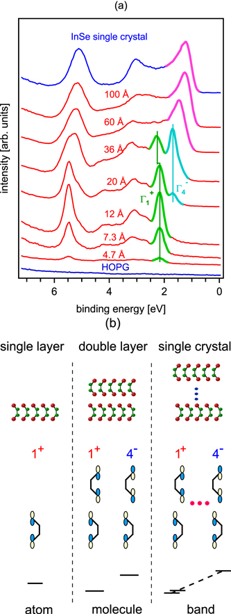
Figure 12. Valence band photoelectron spectra of InSe films deposited on highly oriented pyrolytic graphite for increasing film thickness (a) and evolution of topmost valence levels from atomic-like single layer states to molecule-like double layer states to bulk energy bands (b). (Part (a) reprinted with permission from Ref. 124. Copyright (1998) by the American Physical Society).
Download figure:
Standard image High-resolution imageThe possible absence of coupling of electronic states at interfaces determines whether quantized electronic energy levels are formed in the growing layer. Such quantized energy levels are well known for low-dimensional semiconductor structures.126,127 Energy states are localized within a low-dimensional structure, if the surrounding medium has an energy gap in the corresponding energy range. Electronically decoupled films also lead to the observation of quantized energy levels in thin overlayers with photoemission. Pronounced structures have particularly been reported for Ag on various substrates.128–132 Surprisingly, for Ag films deposited on Si(111) quantized energy levels are observed, although the substrate has no gap in the given energy range.128,132 In this case the lattice mismatch between substrate and film remains as the only explanation for the observation of the localized energy levels. Lattice mismatch evidently leads to a partial reflection of the Bloch wave functions at the interface.e
For van der Waals-epitaxy interfaces, lattice mismatch is also present and in general rather large. One might therefore expect that localized energy levels always show up in the growing films, which would be evident from the thickness dependent changes in electronic structure as described in Fig. 12. But so far such transitions have been found experimentally only, when graphite substrates are used. There are further indications of localized energy levels in GaSe films grown on Si(111),121 but most van der Waals-epitaxy and quasi-van der Waals-epitaxy interfaces show valence band spectra, which are a superposition of bulk substrate and overlayer valence states (see Ref. 6 and references therein). Therefore another mechanism has been discussed as a precondition of electronically decoupled films in van der Waals-epitaxy124: the differences in the electronic structure along z (Γ-A direction of the Brillouin zone, Fig. 3), which is illustrated for InSe, WS2 and graphite in Fig. 13.

Figure 13. Schematic energy bands along ΓA for WS2,52 InSe,56 and graphite.133 The z-states, which are responsible for electronic coupling across the van der Waals-gap, are the 1+, 4−, 2−, and 3+-states (see also Fig. 2).
Download figure:
Standard image High-resolution imageAny interfacial wave function resulting from a coupling of electronic states of the corresponding contact phases will extend on both sides of the interface and needs to follow the local symmetry restrictions. Therefore only such electronic states can couple, which have the same symmetry in both materials. The symmetry labels are indicated in Fig. 13. Although all three materials belong to the same space group and therefore generally have wave functions of the same symmetry, the respective electronic z-states of graphite have very different binding energies. The z-states, which are responsible for electronic coupling, are the 1+, 4−, 2−, and 3+-states (see also Fig. 2). For a large energy difference the electronic overlap will be significantly reduced, which, as a consequence, leads to a decoupling of electronic interlayer interactions. In van der Waals-epitaxy of layered metal chalcogenides the strongest differences in the electronic structures between substrate and layered metal chalcogenide exist for graphite and silicon substrates explaining the observation of electronically decoupled states particularly for these combinations.
The arguments concerning the relative contribution of electronic and structural mismatch are similar to those outlined for the formation of the interface dipole layers at (quasi-) van der Waals-epitaxy interfaces. A final conclusion on the relative importance of these two effects for electronic decoupling cannot be given yet. It is, for example, not clear yet why no indications for electronically decoupled films have so far been observed for the growth of II-VI compounds on van der Waals-surfaces, which also exhibit pronounced electronic structure differences. The reason is probably given by the three-dimensional growth mode of the films, which may lead to too large islands before significant signals of the growing film show up in the photoemission spectra. In addition, the strong valence band emissions of the layered metal chalcogenides make the observation of changes in the electronic structure of growing overlayers more difficult than for graphite substrates, which show no transitions in the corresponding energy regime (see Fig. 12a). It is clearly evident that more detailed experiments are needed with systematic variations of lattice mismatch and electronic structure. But such experiments are difficult and time consuming to perform, as the preparation conditions have to be optimized first for every system.
Getting more detailed insights into the electronic coupling at van der Waals-epitaxy interfaces definitely also requires assistance from theoretical investigations. However, because of the incommensurate interface structures, such calculations are very difficult. Nevertheless, the factors involved in electronic coupling are generally important, since they determine not only the electronic structure of growing overlayers, but most likely also nucleation and initial film growth. The coupling of substrate and overlayer wave functions at the interfaces is also expected to affect charge transport across the interface. These assumptions are indicated by Fig. 5, where different nucleation is observed when InSe is grown under the same conditions on the van der Waals-surfaces of GaSe, MoTe2 and graphite. However, more systematic investigations of the nucleation in dependence on the differences in electronic structure and lattice mismatch between overlayer and substrate are required to verify the underlying dependencies.
Of further fundamental interest is the development of electronic band alignment in the presence of electronically decoupled films. In the case of InSe films one might expect that the energy of the atomic-like single layer state is approximately intermediate between the molecule-like double layer bonding and anti-bonding states. In contrast, the experiment shows a very similar binding energy of the single layer and double layer  -states (see Fig. 12 and Ref. 124). This has tentatively been attributed to thickness dependent changes of the electronic interface dipole.124 A in-depth understanding of this phenomenon might probably also offer an intuitive approach to dipole potential drops at semiconductor interfaces.
Single layer electronic structure
The electronic decoupling of van der Waals-epitaxy films on graphite substrates offers the unique possibility to study the electronic structure of single layers of layered metal chalcogenides. The transition from single layer to single crystal states is already obvious from the normal emission spectra shown in Fig. 12, which have been taken from InSe films deposited on highly oriented pyrolytic graphite (HOPG). Interlayer interactions of layered metal chalcogenides can be studied in more detail if the complete electronic structure of single layers and single crystals are known. Full k-resolved electronic structure measurements are required for this task. Single crystalline films cannot be prepared on HOPG but only on single crystalline graphite. Unfortunately, LEED pattern taken from InSe and SnS2 films deposited onto single crystalline graphite substrates show ring-like diffraction patterns.6 This corresponds to a lack of azimuthal orientation, which is most likely related to the large lattice mismatch in combination with the weak substrate/film interactions.
Highly azimuthally oriented films of WS2 have been prepared on single crystalline graphite.52,125 The films have been deposited using metal-organic van der Waals-epitaxy (MOvdWE) using W(CO)6 and S2 as precursors.134,135 The latter can be obtained by thermal decomposition of pyrite FeS2. Although some residual ring-like diffraction intensity remains in LEED, it has been possible to determine k-resolved valence band spectra for the ΓM and ΓK directions of the Brillouin zone.52,125 Linearly polarized synchrotron light has been further employed to investigate the polarization dependence of the photoionization selection rules, which was used to identify the symmetry of experimentally observed transitions for a comparison with theoretical band structure calculations.
Angle-resolved band structures for single layer WS2 along ΓM and ΓK are shown in Fig. 14. The data are compared to an experimental band structure of a WS2 single crystal in (a) and (b). The experimental single layer and single crystal band structures are almost identical. Remaining differences, as the missing splitting of topmost band near Γ, are explained by the absence of interlayer interactions and by photoionization cross-sections.52 In contrast to the single crystal, the valence band maximum of the single layer is located at the K point of the Brillouin zone as the single crystal ( ) valence band maximum state is absent because of missing interlayer interactions. With this change, a direct optical transition of a single layer of WS2 results as the conduction band minimum of the semiconducting transition metal dichalcogenides is also located at the K point of the Brillouin zone.50,51 It is noted that the electronic states at the conduction band minimum are not affected by the missing interlayer interactions, as the corresponding states are formed by transition metal dxy and
  states, which do not overlap across the van der Waals gap. The transition from a direct to an indirect gap has been observed nearly 20 years later for MoS2 by photoluminescence.136

Figure 14. Experimental band structure of single layer (full symbols) and single crystal (open symbols) band structures of WS2 along ΓM (a) and ΓK (b). A comparison between experimental and theoretical LMTO-ASW band structures (dotted lines) is shown along the ΓK direction for single crystal (c) and single layer (d) WS2.52,125 The valence band maximum of the single layer is located at the K point of the Brillouin zone. As the conduction band minimum is also at the K-point, single WS2 has a direct gap in contrast to the indirect gap of bulk WS2.
Download figure:
Standard image High-resolution imageFigures 14c and 14d shows a comparison of experimental single layer and single crystal band structures with theoretical band structures along ΓK. The theoretical bands are calculated using density functional theory in the local density approximation (LDA) and the scalar relativistic augmented spherical wave (ASW) method with linear muffin tin orbitals (LMTO) (for more details see Ref. 52). The agreement between experimental and theoretical band structure is very good for single crystalline WS2 as shown in Fig. 14c. In contrast, there is less good agreement for the single layer (Fig. 14d). Obviously the calculated band structures show differences between single layer and single crystal, which are not observed in the experiment. This has been attributed to the atomic positions used in the calculation.52 As no structural data exist for the single layer, atomic positions identical to those of the single crystal have been assumed. But smal structural relaxations of the atoms in the absence of interlayer interactions might account for the observed differences between experiment and theory.
To check if relaxation occurs, band structure calculations of single crystal and single layer WS2 including optimization of atomic positions have been performed.137 In this case band structures are calculated using the CASTEP program, which employs pseudopotentials and a plane wave basis set. No evidence for relaxation is deduced from these calculations. Furthermore, the band structures calculated for single layer and single crystal are very similar and also agree with experiments as shown in Fig. 15. Therefore, it is assumed that the differences observed for the ASW calculations are most likely related to the calculational technique. This is supported by a calculation of MoS2 and MoSe2 band structures,64 which also reveal differences depending on the calculation method.

Figure 15. Pseudopotential band structure calculation of single crystal (dotted lines) and single layer (solid lines) WS2 (a). (Reprinted with permission from Ref. 137. Copyright (2002) by the American Physical Society) The lattice parameters were allowed to relax to yield total energy minimization. Comparison of experimental (open circles and triangles) and calculated (open squares) single layer band structures along ΓM (b) and ΓK (c). The dotted lines in (b) and (c) are drawn to interpolate the calculated band structure between the data points.
Download figure:
Standard image High-resolution imageEnergy band alignment
This section describes the energy band alignment at interfaces between different semiconducting layered chalcogenides. The electronic properties of vdWe-heterointerfaces are always deduced in our studies from step-by-step deposited epilayer films analyzed by photoelectron spectroscopy after transfer in integrated cluster tools without breaking vacuum.138,139 With this technique it is possible to follow changes in interface chemistry and surface potentials as a function of film thickness. The investigated interfaces show no indication of chemical interface reactions or adsorbates,6 which would modify the band alignment.140–142
Because of their chemically saturated surfaces, a different interface behavior compared to three-dimensional semiconductors can be expected for layered materials. First studies of band alignment at van der Waals-epitaxy interfaces by photoelectron spectroscopy yield only very small interface dipole potentials, which are within the error limit of the experiment.143,144 This suggests that the band alignment is governed by the electron affinity rule, as it is also observed for interfaces between organic compounds,145,146 which are also characterized by weak chemical interactions.
As typical examples we present in Fig. 16 the semiconductor (quantum) well structures GaSe/InSe/GaSe144 and SnS2/SnSe2/SnS2.147 In the first experiment we have used a single crystal of GaSe with the (0001) surface cleaved in UHV as the substrate and an InSe overlayer has been epitaxially grown in several steps, before GaSe has subsequently been deposited onto the InSe/GaSe layer sequence. The same approach was followed in the case of SnS2/SnSe2/SnS2.

Figure 16. Energy band alignment of GaSe/InSe/GaSe (a) and SnS2/SnSe2/SnS2 (b) quantum well structures determined by photoelectron spectroscopy.144,147
Download figure:
Standard image High-resolution imageFor the GaSe/InSe/GaSe quantum well structure hexagonal LEED-patterns indicate epitaxial growth of the lattice mismatched systems during the whole experiment.144 Very sharp SXPS core level spectra comparable to cleaved single crystals measured with synchrotron radiation further indicate the crystallinity of the grown films. The electronic properties of such interfaces are evidently not affected by large contributions of interfacial defects either related to non-stoichiometry or edge planes nor chemical adsorbates. Therefore, our experiments provide references data compared to interfaces prepared under ambient conditions or with defective van der Waals interfaces.
The band alignment is derived from the experimentally determined core level binding energies.138,139 The resulting valence band offsets are identical for both quantum structures prepared (InSe/GaSe/InSe and GaSe/InSe/GaSe). Both interfaces follow the commutativity rule, which is established by the independence of band offsets on deposition sequence. The values of the conduction band offsets are calculated with the known band gaps. The magnitude of the interface dipole potential is only very small and thus the experimentally determined band alignment follows the electron affinity rule (EAR) within the experimental uncertainty.
A quantum well structure with an inverted ratio of valence band and conduction band offsets is obtained for the SnS2/SnSe2/SnS2 vdWe-system.147 Again we consider an isoelectronic and isostructural combination of materials. In this case also band bending and doping effects can be considered because of the larger thickness of the deposited layers. Again an experimentally determined energy band diagram can be constructed being close to the ideal expectations of 2D van der Waals heterointerfaces. The interface dipole potentials are also close to the expectation of the EAR. In contrast to the GaSe/InSe/GaSe system, where the different energy gaps result in different conduction band energies, a similar difference of the energy gaps of SnS2 and SnSe2 is mostly accommodated by a discontinuity in the valence band. This can be related to the fact that SnS2 and SnSe2 form a common cation (Sn) system, rather than a common anion (Se) system as in the case of the InSe/GaSe heterojunction. Apparently, the common anion (cation) rule for semiconductor band alignment139,148 is also fulfilled for layered chalcogenides, at least for isostructural and isoelectronic systems.
In an extensive evaluation of band alignments at interfaces between semiconducting two-dimensional layered chalcogenides, Schlaf et al. could observe a small but systematic deviation of the band alignment from the electron affinity rule.6,58,149–151 The experimentally determined valence band offsets of a number of vdWe-interfaces is plotted in Fig. 17 vs the offsets expected using a vacuum level alignment and experimentally determined ionization potentials. It is evident that the band offsets show a small but systematic deviation from the electron affinity rule.

Figure 17. Experimental valence band offsets ΔEVB for van der Waals-epitaxy interfaces determined by photoelectron spectroscopy.6,58,149–151 The dashed line corresponds to offsets expected from the electron affinity rule, the full line is a fit to the experimental data. Figure reprinted by permission from Springer Nature Customer Service Center GmbH from Ref. 6, Copyright (2000).
Download figure:
Standard image High-resolution imageThe deviation has been qualitatively related to an electronic dipole potential formed in relation to the model of Ruan and Ching.152 In this model, an interface dipole is formed by tunneling of electrons from the valence bands into the conduction band of the contacting semiconductor. Therefore, its magnitude should depends on the deviation from a symmetric lineup, which is given by valence and conduction band offsets of the same magnitude. The interface dipole δ is then proportional to the deviation from symmetric lineup and given by:

The proportionality constant is determined by fitting the experimental data to Eq. 1, revealing K = 0.09.6,58,149,150 Equation 1 can also be fitted to experimental data of three-dimensional semiconductors, which results in a proportionality constant of approximately twice the value for the layered semiconductors. This difference can qualitatively be understood because the interlayer interactions (electronic coupling) at van der Waals-epitaxy interfaces is small compared to three-dimensional semiconductors, leading to less charge transfer and consequently to smaller double layer potentials. However, the results of Schlaf et al. also show that small electronic interface dipole potentials are also present at van der Waals-epitaxy interfaces. This is a clear proof of the general validity of the induced gap states concept. The smaller magnitude of the charge transfer at van der Waals-epitaxy interfaces is easily understood as a manifestation of the weaker overlap of the substrate and overlayer wave functions as discussed above.
Band Alignment at 3D/2D Interfaces
Schottky contacts
Metals deposited onto layered semiconductors may exhibit different properties. Alkali metals generally intercalate into the van der Waals-gap of the layered materials if deposited at room temperature.153–155 Transition metals generally lead to interface reactions because of their large heat of adsorption (see Ref. 156 and references therein). The sp-metals, i.e. metals without d valence electrons, often form non-reactive and atomically sharp interfaces with a varying tendency to three-dimensional island growth.67,68,72,74,78,156 It has been stated that the barrier heights for such metals on semiconducting layered chalcogenides follow the Schottky-limit, indicating a validity of the electron affinity rule.68,72,74,157
Schottky barrier heights of In, Cu, Au, Pt, on p-type and n-type WSe2 single crystals are shown in Fig. 18. In general a high work function metal gives a larger barrier height on n-type WSe2 as expected. The barrier height of In on p-WSe2 is given by ΦB, p = 1.03 eV,74,156 which agrees with the difference of the semiconductor ionization potential (IP(WSe2) = 5.2 eV) and the metal electron affinity (χ (In) = 4.2 eV). However, the other metals form p-type barrier heights, which are approximately 0.7 eV higher than the corresponding difference as indicated by the dotted lines in Fig. 18.

Figure 18. Schottky barrier heights on p- and n-WSe2 in dependence on metal work function.156 Stars correspond to work functions of (111) surfaces of the metals and diamonds to polycrystalline metal work functions. The ionization potential and electron affinity are given with error bars as the work functions ϕ(p-WSe2) and ϕ (n-WSe2), respectively.
Download figure:
Standard image High-resolution imageThis result is difficult to understand in terms of the interface dipole potentials discussed in terms of the induced gap states model.158–160 Any of the described dipoles would lead to lower barrier heights compared to the electron affinity rule as a part of the contact potential difference is compensated by the dipole potentials induced by the formed interface states. In contrast, the barrier heights would follow the Schottky limit if the work function of WSe2 is taken 0.7 eV larger than measured values (or the metal work function is 0.7 eV lower than the measured values).
This modification of barrier heights might be attributed to a lowering of the surface dipoles of the metals, which considerably contributes to the work function161: If the spill-out of wave functions at the interface is considerably reduced compared to the free surface, this would lead to a lower metal work function. To finalize this explanation of the data in Fig. 18 more systematic studies on Schottky barrier heights on layered semiconductors and, even more important, theoretical investigations would be required.
The large interface dipole potential is not the only surprising result obtained for Schottky barriers on layered materials. Schottky barrier heights of different semiconductors with the same metal (mainly Au or Al) are sometimes used to predict the band alignment at semiconductor heterojunctions.162,163 This procedure is based on the transitivity of band alignments and related to the fact that band offsets and Schottky barriers are governed essentially by the same alignment of charge neutrality levels.158,160,164 The p-type Schottky barrier height of Au on WSe2 amounts to 0.76 eV.75,156 Measurements of InSe/Au Schottky barrier formation give values ranging from 0.2–0.7 eV (see compilation of data in Ref. 6). Together with the valence band offset between InSe and WSe2 of ΔEVB = 0.4 eV165 (see also Fig. 17) this corresponds to a deviation from transitivity of at least 0.45 eV. The barrier heights of the sequence Au/WSe2/InSe/Au are illustrated in Fig. 19.

Figure 19. Non-transitivity of Schottky barriers on layered semiconductors. In the sequence Au/WSe2/InSe/Au the deviation amounts to 0.45–0.95 eV, depending on the value used for the InSe/Au Schottky barrier height.
Download figure:
Standard image High-resolution imageThere has been an attempt by Mönch to attribute the Schottky barrier heights of layered semiconductors to metal induced gap states using an electronegativity approach.163 The results presented in Figs. 18 and 19 disagree with the suggestion by Mönch. His concept, that charge transfer at interfaces is strongly related to the difference in electronegativities, can be successfully applied to three-dimensional materials. But this approach is not appropriate for interfaces including the chemically saturated van der Waals-surfaces of layered materials, since no (strong) covalent chemical bonds can form at these interfaces.
Interfaces with II-VI semiconductors
Experimental results
The growth of II-VI semiconductors on layered metal dichalcogenides is characterized by a strong tendency of three-dimensional island growth, which is due to the strong chemical bonds within the II-VI compounds and the small adhesive energy on the van der Waals-surface. A lowering of the surface energy is hence achieved by island formation. For the use of layered materials as buffer layers in in 3D/2d/3D systems, preferentially single crystalline layers should be formed. This is generally not possible with island growth, since the formation grain boundaries has to be expected during island coalescence with increasing film thickness. There are also two different growth domains found on the surfaces, which are rotated by 180° (see Fig. 9). Although single crystalline growth of three-dimensional materials on the van der Waals-surface has not yet been achieved by using qvdWe approaches, it has been possible to investigate the electronic properties of these interfaces.
The band alignment at interfaces between layered semiconductors and II-VI compounds has been studied by Löher et al.,90,94,151,166 and by Wisotzki et al.167 On transition metal dichalcogenides like MoTe2 and WSe2 large interface dipoles of the order of ∼1.1 eV for CdS and of ∼0.8 eV for CdTe are observed.166 In addition to the interfaces studied by Löher et al., an interface dipole of 0.6–0.7 eV has been determined at the WSe2/ZnSe interface. Energy band diagrams of the investigated interfaces are given in Fig. 20a. In contrast only small interface dipoles of <0.3 eV have been determined for CdS and CdTe on InSe94 and for ZnSe on InSe and GaSe,167 as shown in Fig. 20b.

Figure 20. Band alignment at interfaces between layered semiconductors and II-VI semiconductors (a) transition metal dichalcogenides,166 (b) III-VI compounds.94,167 All values are in eV. Band bending is not shown.
Download figure:
Standard image High-resolution imageAs a consequence, a fundamental difference between quasi van der Waals-epitaxy interfaces of the layered transition metal dichalcogenides (TMDC: WSe2, MoTe2) and of the III-VI compounds (InSe, GaSe) is suggested. Larger interface dipole potentials are observed for the transition metal dichalcogenides, for both metallic and II-VI contact partners. The different interface dipole potentials for II-VI films, comparable to the non-transitivity observed for metal contacts shown in Fig. 19.
The structural dipole model
The origin of the large interface dipole potentials at TMDC/II-VI interfaces has been related to the orientation of the growing overlayer. Although strong clustering of the II-VI films occurs, the overlayers grow with their three-fold  (for zincblende) or six-fold
  (for wurtzite) symmetry axis perpendicular to the van der Waals-surface.71,92,94,167 These directions are polar directions with alternating layers of positively and negatively charged atomic planes, which induce an alternating electrostatic potential and result in different electron affinities of the cation and anion terminated (111) surfaces.168–170 A sketch of the band alignment at interfaces between II-VI compounds and layered semiconductors including these structural dipoles is given in Fig. 21.

Figure 21. Band alignment at MX2/II-VI (M = W, Mo; X = S, Se, Te) interfaces given by Löher et al.94,166 The structural dipole δ of the polar II-VI compound can be split into a contribution eDi at the inner interface and a contribution at the vacuum interface eDv. Since the growth of the II-VI compound starts with the cation terminated surface, which has a low electron affinity χ(111), a large electron affinity  is present at the anion terminated vacuum surface. The structural dipole mainly accounts for difference in χ between substrate and film. Only small electronically induced interface dipoles eDe have to be taken into account.
Download figure:
Standard image High-resolution imageThe large interface dipole potentials at the TMDC/II-VI interfaces correspond to a particular orientation of the II-VI layer, where the (low electron affinity) cation terminated surface is adjacent to the substrate and the (high electron affinity) anion terminated surface forms the growth front. This assumption is confirmed by (i) the large ionization potentials measured for the surfaces of the II-VI films and (ii) the observation of facets on the film surface.94,166 The first observation is clearly connected to the anion terminated surface with the negatively charged planes on top. In addition, facetting is reported for the anion terminated  or
or  surfaces.171
The magnitude of the internal structural dipole for CdS and CdTe can be estimated based on the differences of the electron affinities for GaAs(111) and GaAs  , which has been measured by Ranke.168 The experimental value for GaAs of Δχ111 = 0.4 eV has been scaled by using material specific ionicities (from Ref. 172) and lattice parameters resulting in Δχ111 = 0.6, 0.8 eV and 0.75 eV for CdTe, CdS and ZnSe, respectively.166 For CdTe and CdS the experimental values are 0.2–0.3 eV larger (Fig. 20a), which could possibly be explained by an additional electronic interface dipole as indicated by "eDe" in Fig. 21. This electronic interface dipole is then of the same order of magnitude as the dipoles observed at interfaces between two layered compounds.
The structural dipole model for the band alignment at interfaces between II-VI semiconductors and layered metal chalcogenides is basically a modification of the electron affinity rule, which considers two additional contributions to the lineup: electronic dipole potentials, which are always present but are considered to be small at (quasi-) van der Waals-epitaxy interfaces, and the structural dipole, which results from the alternatingly charged atomic planes in the  or
or  growth direction of the II-VI semiconductors. As long as the interface is atomically abrupt (as assumed in Fig. 21b), the structural dipole should not form on the van der Waals-surface of layered substrate but only in the II-VI overlayer. This seems to be true for different TMDC substrates, but evidently not for all layered semiconductors (see Fig. 20b). A first explanation for the smaller dipoles at III-VI/II-VI interfaces is based on structural arguments94: The lattice constants of InSe and CdS are very close. A different interface structure, where the first Cd plane can penetrate into the Se surface plane, is therefore possible. In this case a partial screening of the positive charge of the Cd can occur, resulting in a smaller interface dipole. However, this explanation cannot account for all of the investigated interfaces, since the InSe/CdTe and GaSe/ZnSe interface exhibit a large lattice mismatch but also show only small interface dipoles. Consequently the structural dipole model proposed by Löher et al. cannot consistently explain the interface dipole potentials at layered semiconductor/II-VI interfaces.
An electronic dipole model
In this section a alternative model to describe the band alignment at quasi-van der Waals-epitaxy interfaces is presented. The model does not take structural dipoles into account, but rather considers electronic interface dipoles. Electronic interface dipoles are related to the local interactions at the interface.158–160 Charge transfer across an interface, which is the origin of this dipole, occurs from occupied orbitals on one side of the interface to unoccupied orbitals on the other. Significant charge transfer occurs only if the respective orbitals exhibit small energy differences and large spatial overlap. The smallest energy differences between occupied and unoccupied energy levels in solids is possible for electronic states close to the Fermi energy, which correspond to states close the energy gap in semiconductors. Understanding the dipoles at quasi-van der Waals-epitaxy interfaces therefore requires a detailed description of the symmetry, energy levels and orientation of the respective orbitals. In the following we will discuss the involved charge transfer for the layered dichalcogenides of group VIb transition metals (WSe2 and others), the layered III-VI compounds (InSe,GaSe) and the (111) surfaces of zincblende compounds.
The electronic structures of the layered materials as described below are strictly valid only for bulk materials. At quasi-van der Waals epitaxy heterointerfaces the interactions may be different from those across the van der Waals-gap in bulk material, but it is assumed that the structure of the van der Waals-surface does not change during interface formation. Basically, the interlayer interactions are absent at the surface, which should lead to a modification of the respective electronic states as discussed in Ref. 52. The energy levels of the involved states are expected to be situated within the range of the interlayer energy splitting, which corresponds to the energy dispersion along the ΓA direction of the hexagonal Brillouin zone.52,124 As the dispersion along ΓA is generally small, the electronic states interacting at an interface should have energies close to the bulk pz and/or  -states.
The (111) surfaces of compound semiconductors.—The surface electronic structure of the (111) surfaces of II-VI compound semiconductors is influenced by the surface reconstruction. Reconstructions of polar surfaces are a consequence of the surface charge of ideally bulk terminated surfaces, which are electrostatically unstable170 in analogy to polar interfaces between heterovalent semiconductors.173,174 For the hexagonal symmetry of the van der Waals-surfaces and the experimentally observed (111) or (0001) orientation of the growing overlayers, one has to distinguish between the cation terminated (111) (or (0001)) and the anion terminated  (or (
(or ( ) surfaces of the zincblende (or wurtzite) crystal structures. The cation and anion terminated surfaces are not equivalent because of the alternating distance of the cation and anion (111) planes.
In Fig. 22a the structure of the ideal bulk terminated zincblende (111) surface is shown. The (111) surfaces of III-V semiconductors usually show a 2 × 2 reconstruction.171 A cation vacancy model (or vacancy buckling model) as sketched in Fig. 22b, is the accepted structural model for the 2 × 2 reconstruction of III-V (111) surfaces (for example for GaAs).175–177 The model is consistent with STM images178 and gives the lowest surface energy as long as the chemical potential of the anion (As) is not too high.177 In the cation vacancy model one of four surface Ga atoms is removed, resulting in three Ga and three As dangling bonds per 2 × 2 unit cell. The Ga dangling bonds are directed toward the surface while the dangling bonds of the As atoms adjacent to the vacancy are oriented parallel to the surface toward the Ga vacancy.

Figure 22. Zincblende(111) surfaces: ideal cation vacancy (vacancy buckling) model for (111)—2 × 2 surface (b) and adsorbed anion trimer model for  .
.
Download figure:
Standard image High-resolution imageA relaxation of the Gallium atoms toward the As plane and of the As atoms toward the Ga vacancy is decuded from total energy minimized surface energy calculations.176,177 This relaxation leads to an approximate sp2 configuration of the Ga atoms and an approximate pyramidal coordination of As. Corresponding surface relaxations leading to a comparable electronic configuration are observed for all (110) surfaces of III-V and II-VI compounds.160,171 This relaxation leads to an upward shift of the Ga dangling bond energy and a downward shift of the As dangling bond energy and consequently to transfer of electrons from the Ga to the As dangling bonds. Roughly speaking all cation dangling bond states are empty and all As dangling bonds are doubly occupied. This general behavior has been condensed in the so-called electron counting rule,111 which is an easy rule for determining possible surface structures at semiconductor surfaces and which guarantees that the surfaces are not charged and therefore are electrostatically stable.
A 2 × 2 reconstruction is also observed for the As terminated  surfaces of GaAs.171 In analogy to the (111)—2 × 2 surface an uncharged surface would be consistent with an anion vacancy reconstruction. However, for a large range of the As chemical potential an adsorbed trimer structure as shown in Fig. 22c is thermodynamically more stable.177 An As trimer model is also consistent with STM measurements of MBE grown GaAs
  surfaces.179 The 2 × 2 surface transforms with heating into a
  reconstruction before Ga precipitation occurs. For other III-V compounds other surface reconstructions are observed in addition, which are, however, less well understood than those of GaAs.
Only very few data are available on surface reconstructions of II-VI semiconductors.171 CdTe, ZnSe and ZnTe (111) surfaces also show 2 × 2 reconstructions in LEED.180 Although not explicitly stated in the literature, a cation vacancy structure is also likely for those materials, as the electron counting rule is satisfied by such a structure. Further evidence for this assumption is given by the similarity between the reconstructions of the II-VI and the III-V (110) surfaces.171 The  surfaces of II-VI semiconductors are distinct from those of the III-V compounds. 1 × 1 reconstructions with {110} and {331} facets are reported for CdTe, ZnSe and ZnTe.180 Facetted surfaces are also observed with LEED during growth of II-VI compounds on layered semiconductors.181 However, in the presence of facetting, reconstructions might be difficult to identify. It is not clear if the differences between the III-V and II-VI
  surfaces are due to different surface preparation conditions. The II-VI surfaces investigated in Ref. 180 have been prepared by sputtering and annealing, while the III-V surfaces are often prepared by molecular beam epitaxy.
A detailed electronic band structure calculation for a (111) surface is given for GaAs(111) by Henk and Schattke.182 As a result of the reconstruction the Ga dangling bonds are shifted upwards in energy to 1.7 eV above the valence band maximum. Several filled surface state energy bands are identified, which basically agree with angle-resolved photoemission data.183 For binding energies between 0–2 eV with respect to the valence band maximum there are four occupied surface state bands. These are dominated by As px and py-orbitals, since the dangling bond states point toward the Ga vacancy. However, also contributions from As pz-orbitals to these surface states are found.182 According to Henk and Schattke the largest contribution of z-states results from the As atom, which is not in the neighborhood of a vacancy. Other surfaces states with higher binding energies have large contributions from atoms of the 3rd and 4th atomic planes and will therefore not contribute to the charge transfer at the quasi-van der Waals-epitaxy interfaces.
The charge transfer.—At an interface charge transfer in both directions is in principle possible (bonding and back bonding) if the corresponding electronic states exist. For the argumentation given below, it is assumed that the electronic structure of the (111) or (0001) surfaces of II-VI compounds adjacent to the van der Waals-surfaces corresponds to those of the GaAs(111) − 2 × 2 surface, because of the lack of other data.
At interfaces between the van der Waals-surfaces of group VIb transition metal dichalcogenides with the hexagonal surfaces of II-VI compounds, electron transfer from the TMDC to the II-VI semiconductor is easily accomplished from the occupied  and pz-states at the valence band maximum of the TMDC to the unoccupied cation (Cd, Zn) dangling bond states. The latter have energies close to the conduction band minimum of the II-VI semiconductor. Back bonding is much less probable at these interfaces since (i) the occupied surface states of the II-VI's are dominated by px and py-states and (ii) the conduction band states of the TMDCs are also dominated by x, y-states. Overlap between orbitals, which are directed parallel to the interface can be expected to be very low.
It has been discussed above that there are also small contributions of metal  -states to the TMDC conduction band. It is expected that these states do not lead to a significant charge transfer across the interface, since these atoms are located in the second atomic layer and shielded by the chalcogen atoms. Therefore overlap of occupied II-VI-states with unoccupied TMDC-states will be small. The (bonding) charge transfer
  is therefore expected to be considerably larger than the (back bonding) charge transfer
  . Orbital symmetries and expected magnitude of charge transfer at TMDC/II-VI semiconductor interfaces is sketched in Fig. 23a.

Figure 23. Charge transfer at layered semiconductor/II-VI interfaces. (a) Layered group VIb transition metal dichalcogenides (MoS2, WSe2 et al.), (b) layered III-VI compounds (InSe, GaSe). The estimated relative magnitude of charge transfer is indicated by the arrow thickness and number of charges.
Download figure:
Standard image High-resolution imageInteractions are different at interfaces between II-VI semiconductors and III-VI layered chalcogenides InSe and GaSe. As for the TMDCs charge transfer  is easily accomplished from the chalcogen pz-orbitals to the cation dangling bond states. In contrast to the TMDCs the conduction band minimum of InSe and GaSe has also large contributions from chalcogen pz-orbitals and electron transfer
  is consequently not forbidden by symmetry. However, the symmetries of the occupied II-VI surface states would still allow only for a reduced overlap, resulting in a smaller back bonding charge transfer. Although there is still a net charge transfer from the layered semiconductor to the II-VI compound, a smaller overall interface dipole can be expected compared to the interfaces between TMDCs and II-VI semiconductors. A schematic representation of the interfaces between layered III-VI compounds and II-VI semiconductors together with the resulting charge transfer is summarized in Fig. 23b.
By considering the electronic structures of layered chalcogenides and of II-VI surfaces it is now possible to qualitatively explain (i) the large magnitude of the interface dipole potentials for the layered group VIb transition metal dichalcogenides and (ii) the difference of interface dipole potentials between the TMDCs and the III-VI compounds. For both materials transfer of electrons from occupied valence states into unoccupied states of the II-VI semiconductor surface is easily accomplished, while the reverse transfer is strongly hindered for the TMDCs and at least less probable for the III-VI compounds. In both cases a net interface dipole with its negative end at the II-VI compound is induced. It is larger for TMDCs, which agrees with the experimental observations.
Structural vs electronic dipoles
As outlined above the interface dipole potentials observed at layered semiconductor/II-VI interfaces are probably largely caused by charge transfer across the interface due to overlapping frontier orbitals. The electronic dipole model contradicts the previously suggested structural dipole model,94,166 in which the interface dipole potentials are generated by the large internal dipole between the cation and anion planes (see Fig. 21). Structural dipoles depending only on the polarity of II-VI semiconductor cannot explain the large difference of interface dipole potentials observed for interfaces of TMDCs and of III-VI compounds. They can also not explain the large interface dipole potentials at Schottky barriers of layered semiconductors, as metals should not provide an internal structural dipole.
In contrast, electronic interactions can at least qualitatively explain the differences of interface dipole potentials observed between II-VI semiconductors and TMDCs and III-VI compounds, as outlined above. The non-transitivity of Schottky barriers Au/WSe2/InSe/Au (see Fig. 19) is possibly also a consequence of different dipoles at the TMDC/Au and III-VI/Au interfaces. It is thus suggested that the electronic charge transfer model presented here for layered semiconductor/II-VI compound interfaces, might also apply for layered semiconductor/metal interfaces. Because of the very small dipole potentials at interfaces between two layered semiconductors (see Fig. 17), the difference of the interface dipole potentials at TMDC/II-VI and III-VI/II-VI interfaces of 0.6–0.8 eV, corresponds also to a non-transitivity of band alignment in the series II-VI/TMDC/III-VI/II-VI. This non-transitivity is of the same magnitude as the non-transitivity of Schottky barriers (see Fig. 19).
A detailed analysis of the interactions at layered semiconductor/metal interfaces in terms of symmetric and electronic properties of frontier orbitals as outlined in this section for the interfaces with II-VI compounds, would depend on the metal. Noble metal (111) surfaces, for example, have energy gaps of the order of 5 eV and the Fermi energy is situated at 0.85, 0.3, and 1.0 eV above the bottom of the gap for Cu, Ag and Au, respectively.184 A surface state energy band crossing the Fermi energy exists within this gap. The energy dispersion of occupied and unoccupied parts of the surface state energy band on Cu(111) has also been determined by Crommie, Lutz and Eigler using voltage dependent scanning tunneling microscopy.185 For Cu, the surface band is formed by Cu s and pz-orbitals. Therefore, both occupied and unoccupied energy levels exist at the surface close to the Fermi energy, enabling charge transfer in both directions.
The influence of lattice mismatch on the band alignment has not been considered yet in our discussions. Lattice mismatch between the layered substrates and the II-VI overlayers would not affect the structural dipole of the II-VI film. In contrast, orbital overlap across the interface would be strongly reduced. In the presence of lateral mismatch favourable atomic positions, which allow for large charge transfer, do only exist for a fraction of the interface plane. Electronic interface dipole potentials of up to 1 eV may therefore not be possible for quasi-van der Waals-epitaxy interfaces. Interface dipole potentials above 1 eV are hardly observed even at covalently bound interfaces between three-dimensional semiconductors.174,186,187
The electronic dipole is formed by an unusual interfacial charge transfer, which is modified by the dielectric constant .159,188 At an interface, two different materials contribute to the dielectric response. For interfaces between three-dimensional semiconductors an average of the dielectric constants of the two materials is basically used, as no unique definition of exists for interfaces. This procedure might not apply to weakly interacting interfaces like in the present case. In the absence of strong chemical bonds the polarizability and hence could be reduced. One may now speculate that large interface dipole potentials can exist at lattice mismatched quasi-van der Waals-epitaxy interfaces despite the reduced charge transfer, due to the reduced screening of the dipole. Therefore large electronic interface dipole potentials might be reasonable for these interfaces.
In summary, no final conclusion on the relative contributions of structural and electronic interface dipoles to the band alignment at quasi-van der Waals-epitaxy interfaces can be given yet. Although the suggested electronic dipole model might describe a larger number of interfaces, some doubt about the magnitude of the dipole remains. However, the basic validity of the electronic dipole model is indicated by the analogy to the electronic interface dipole formed at van der Waals-epitaxy interfaces.
Another assumption made is that no chemical decomposition of the layered substrates occurs, which could definitely also account for different interface dipoles. There is evidence that the interfaces are atomically abrupt,6 as implicitly assumed throughout this chapter. Experimental investigation of further material combinations might put the argumentation on a more sound basis.
Electronic Structure of Si(111):GaSe
Surface passivation
Chemical passivation of semiconductor surfaces is an important research topic in materials science and technology. Hydrogen termination of silicon is widely used to prevent surface oxidation of Si by a saturation of the surface dangling bonds via the formation of Si–H bonds. Mostly electrochemical preparation routes are applied. The most simple procedure is dipping a Si wafer into hydrofluoric acid, which also removes oxides from the surface, but improved passivation can be achieved with more elaborate processes as described in Ref. 189. Hydrogen terminated silicon wafers can be handled in air for several minutes only, before oxidation sets in. In contrast, it has been shown that GaSe covered Si(111) surfaces show almost no oxidation even after 30 days storage in air.190 The GaSe termination layer is stable up to temperatures above 500 °C.110,119 When a Si:H surface is exposed to a GaSe flux at elevated temperature below the desorption temperature of monohydrides (Si–H), the Si–H bonds are replaced by the Si–Ga–Se bonds. These results indicate that the Si:GaSe surface forms a thermodynamically very stable surface termination layer.
Also electronic passivation of the Si(111):GaSe surface has been proven by photoemission.191 In these experiments, the GaSe half-sheet termination layer was prepared by a stepwise deposition of Ga and Se onto a Si(111)-7 × 7 surface. This procedure for preparation of the Si(111)-GaSe van der Waals surface termination is not ideal, as it is accompanied by several structural rearrangements of the Si and Ga atoms at the surface, most likely leading to an incomplete coverage.192 However, it allows to follow the evolution of the surface potentials during deposition as shown in Fig. 24, giving more insight into the chemical bonds at the surface.

Figure 24. Surface potentials during preparation of the Si(111):GaSe surface: (a) n-Si(111)-7 × 7, (b) with monolayer Ga coverage and (c) n-Si(111):GaSe. (Reprinted from Ref. 191, with the permission of AIP Publishing).
Download figure:
Standard image High-resolution imageCompared to other silicon surface terminations by hydrogen193 or arsenic,194 the GaSe surface termination shows no evident surface core-level shift of the Si 2p level indicating the formation of a non-polar Si–Ga chemical bond despite the electronegativity difference of Si and Ga. This can be rationalized in the following way: Deposition of only Ga leads at first to a decrease of the electron affinity as shown in Fig. 24b. This corresponds to a surface dipole with its positive end toward vacuum or a charge transfer from Ga to Si, in agreement with the larger electronegativity of Si. But selenization of the Si(111):Ga surface leads to a strong increase of the electron affinity. The reversal of the surface dipole is explained by charge transfer from Ga to Se, which is even more electronegative than Si. As the polarity of the Ga–Se bond leads to a strong charge transfer from Ga to Se, the positive charge at the Ga atom is lowered and eliminates the polarity of the Si–Ga bond.
The Si(111):GaSe surface shows nearly flatband conditions as no band bending remains at the Si(111):GaSe surface.191 The Si dangling bond states situated close to midgap on the (111) surface are electronically saturated by forming the Si–Ga–Se surface bonds and lead to a low density of electronic surface states in the bandgap. Although it cannot be directly quantified from the PES measurements, the flatband condition indicates a surface state density of the order of those observed at Si(111):H surfaces (<3 × 1010 cm−3).189,195
The electronic valence band structure of the surface, which is discussed in the following section, can thus be described by an almost undisturbed GaSe band structure, where the Ga–Ga bond is replaced by the Si–Ga bond leading to an almost one-to-one replacement of the corresponding energy levels. This further establishes the non-polarity of the Si–Ga bond in the Si(111):GaSe half-sheet van der Waals surface termination. In combination with the chemical inertness and temperature stability of the surface, which is superior to any other Si surface terminations, the GaSe termination layer generates an exceptional Si(111) substrate to be used for Si based heterostructure devices.
Band structure
The electronic band structure of Si(111):GaSe has been determined by angle-resolved and energy dependent valence band photoelectron spectroscopy (ARPES) using synchrotron radiation. Measurements have been performed in our group121 and by the group of M. Olmstead at University of Washington, Seattle (USA).196 Details of the ARPES technique can be found in Ref. 197. A complete interpretation of the spectra is presented here for the first time.
Normal emission spectra probe the electronic structure perpendicular to the surface. This corresponds to the ΓL direction of the silicon Brillouin zone197 and to the ΓA direction of the hexagonal GaSe Brillouin zone. The latter is identical to those of WS2, which has been displayed in Fig. 3. In Fig. 25a normal emission valence band spectra, as obtained using excitation energies hν = 14–30 eV, are presented. The observed electronic transitions (peaks and shoulders) can be plotted vs wave vector as done in Fig. 25b, where the perpendicular component k⊥ of k has been determined assuming direct transitions to free electron final states with an inner potential of 12.5 eV. Values of k⊥ are further reduced to the first Si Brillouin zone.

Figure 25. Normal emission valence band spectra of Si(111):GaSe in dependence on indicated photon energy (a). Binding energies of transitions vs reduced wave vector k⊥ (b). The reduced k was calculated using free electron final states and an inner potential of 12.5 eV.198 Filled symbols correspond to peaks, open symbols to shoulders in the spectra. Circles are from spectra taken with photon energies hν = 63–165 eV and squares from photon energies hν = 14–30 eV energy.
Download figure:
Standard image High-resolution imageThe binding energy of most of the transitions deduced from normal emission photoemission do not depend on k. Such dispersion-less states are expected for surface state emissions. Only some reminiscences of Si bulk states are observed. The fact that surface state emissions dominate the spectra is not surprising as the GaSe half-sheet is almost as thick as the minimum of the photoelectron escape depth, which is attained at ∼50 eV electron kinetic energy.199
In Fig. 26 binding energies of electronic transitions obtained from angular dependent valence band spectra taken with hν = 21 and 72 eV are shown along the ΓM symmetry direction.121,196,198 An experimentally determined band structure obtained from a vacuum cleaved GaSe single crystal is shown for comparison.121 There is a striking similarity between the GaSe and the Si(111):GaSe band structures, which will be explained in more dtail in the following discussion by considering the molecular orbital contributions to the states involved in the respective transitions for GaSe and the changes expected at the half-sheet layer. The theoretical band structure given by the semiempirical tight binding calculation of Doni et al.56 will be used for comparison. Their calculation shows no systematic deviation to a more recent band structure calculation by Gomes da Costa et al.,57 but provides more details about the origin of the electronic states. The calculated GaSe band structure is presented in Fig. 27.

Figure 26. Electronic structure along ΓM of a GaSe single crystal (a) and of Si(111):GaSe (b) and (c).198 The band structures are determined from angle-resolved valence band spectra taken with hν = 21 eV (a)+(b)121 and hν = 72 eV,196 respectively. Filled circles correspond to pronounced emission structures, open circles to weaker structures.
Download figure:
Standard image High-resolution image
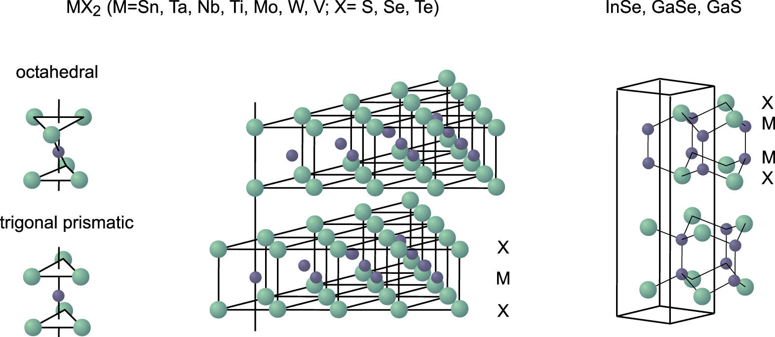
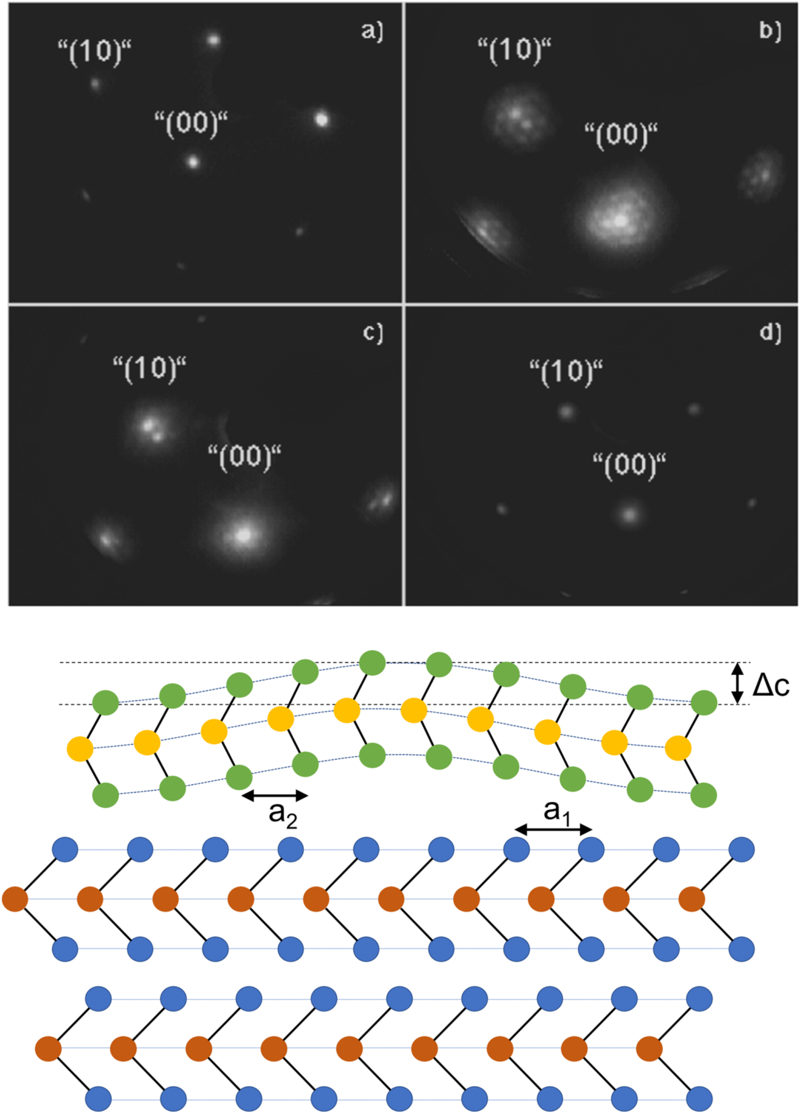
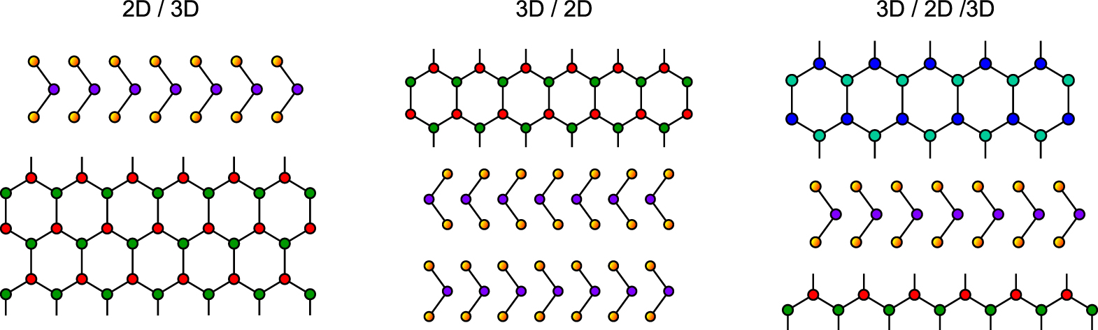
Figure 27. Semiempirical tight binding band structure of GaSe along ΓM according to Doni et al. (a) Ref. 56. Upper and lower limits of the color-shaded areas correspond to energy bands in the central ΓM plane of the hexagonal Brillouin zone and indicate inter-layer splitting and red lines approximately halfway between the upper and lower limits to dispersion in the top plane of the Brillouin zone (along AL). Lines given in (b) indicate the dispersion of energy bands in the hypothetical absence of hybridization. Corresponding lines in (c) are tentative non-hybridized energy dispersions for a hypothetical isolated Ga–Se half-sheet. The bonding/antibonding splitting of the Ga–Ga bond is indicated by the arrows and should not occur for an isolated half-sheet.
Download figure:
Standard image High-resolution image
In normal emission ultraviolet photoelectron spectra of III-VI compounds, emission features involving four groups of bands are observed, which are labelled A to D (see Fig. 26 and Refs. 124, 200, and 201). In normal emission from van der Waals-surfaces, the observed transitions involve only electronic states with k vectors along ΓA. Groups of bands (A-D) are also indicated on the left of Fig. 27a. The molecular orbital character of the corresponding states at Γ and A is given as Se pz (A), px and py (B), and Ga s (C, D).55,56 The Ga s-orbitals form bonding (D) and antibonding (C) combinations with respect to the Ga–Ga bond.
Because of hybridization the energy levels derived from certain orbital combinations do not directly correspond to the calculated energy bands. In terms of energy band structure a crossing of bands is only allowed, if they have different symmetry, i.e. they do not interact (hybridize). In contrast, the hybridization of energy bands leads to an energy gap. With the help of tabulated symmetrized combinations of atomic orbitals and critical point symmetry labels,56 hypothetical energy bands without hybridization can be drawn for bulk GaSe. The result is shown in Fig. 27b. The construction of non-hybridized energy bands is easily accomplished for the ΓM direction, which corresponds to the crystallographic y-axis (see Fig. 27d).f The given hypothetical energy bands show the dispersions expected from simple tight binding considerations.53
Of interest in the present context are those electronic states, which are expected to persist for an isolated half-sheet layer. These can, at least partly, be a priori identified. First of all, interlayer interactions, which are indicated in Fig. 27 by the shaded grouping of bands, have to be omitted (see the Section on the electronic structure of layered chalcogenides and Ref. 52). In addition, cutting the layer between the two Ga atoms will also modify the intralayer interactions mainly affecting the z-states and removing the (small) splitting between the x+ and x−-states (see Fig. 2). No strong changes of the energy dispersion of Se px and py-bands are expected on the other hand, since the distance between the two Se sheets within a single layer are rather large and hybridization of the chalcogen px and py-states with the Ga px and py-states is still possible and not strongly modified, because of the almost unchanged Ga–Se bond length and geometry.
Based on these considerations, tentative energy bands for a hypothetical isolated GaSe half-sheet layer are drawn in Fig. 27c. As argued above, the px and py-bands are not modified (bands III and IV). The Ga–Ga bonding and antibonding states (groups C and D at Γ) are represented by dashed lines in Fig. 27c. As there are no Ga–Ga bonds the splitting should be absent for an isolated half-sheet layer and the two bands are replaced by a single band approximately half-way between the dashed bands, as indicated by a solid line dispersing upwards along ΓM. The situation is more complicated for the pz-state, which forms the valence band maximum, as the Ga–Se pz intralayer overlap is still existent (compare Fig. 27d). It is remembered that the experimentally observed energy bands should follow the dispersion of hybridized bands. The construction of non-hybridized bands is just meant to more easily identify those parts of the GaSe band structure, which can be expected to persist at the half-sheet layer.
The px and py-states give rise to strong emission from the Si(111):GaSe surface at a binding energy of BE ≈ 3 eV at Γ (see Figs. 26b and 26c). Around BE = 8 eV at M the py-states are also clearly present. The px-states at M contribute to the number of transitions observed at the expected binding energies. Furthermore the Si(111):GaSe surface also shows emissions both at Γ as well as at M at binding energies, which agree to those of the single crystal Ga–Ga bonding and antibonding states. These emissions are therefore most likely attributed to the replacement of the Ga–Ga bond with the Ga-Si bond. Hence, the binding energies of the bonding and antibonding Ga-Si states of Si(111):GaSe agree with those of the Ga–Ga states measured at GaSe single crystals. This confirms the non-polarity of the Ga-Si bond at this surface, as also deduced from the absence of a Si surface core-level shift.191
Transitions with lowest binding energies emerge from the topmost valence band, which is the  state at GaSe single crystals. Respective emissions are also clearly observed from Si(111):GaSe with the only difference of missing interlayer splitting. Hence, also these states are only little affected by putting a half-sheet of GaSe on top of the Si surface. The expected upward dispersion of unhybridized pz-states with increasing k∥ is not observed. The missing upward dispersion of the valence band maximum state for k∥ > 0 at GaSe single crystals, which is a consequence of hybridization between pz and px, py,g is therefore also missing at Si(111):GaSe. This could have been expected from the minor changes of the symmetry of the layer. It has an important consequence, as it produces a surface without electronic states within the Si bandgap, leading to an electronically passivated surface.
Conclusions
The concept of van der Waals-epitaxy has been introduced by Koma in 198548 and was followed by a number of people since then mostly because of fundamental interest in the specific properties of van der Waals surfaces, interfaces and thin films (see Ref. 6). Since then epitaxial films of a variety of different layered chalcogenides have been prepared. Also quasi-van der Waals-epitaxy between two-dimensional and three-dimensional materials has been widely studied. Most of these studies were using growth conditions which lead to a homogeneous, statistically distributed nucleation on the van der Waals substrate plane. As a consequence, mostly the control in the formation of nicely grown epitaxial overlayers have been in the focus of the past research and attempts of spatially controlled nucleation with subsequent control of well-defined lateral film growth was not in the center of interest at this time. Therefore, the understanding of the basic growth and nucleation mechanisms is still at the beginning and mainly relies on the general concept of surface tensions.6 However, the few existing investigations of initial growth in van der Waals-epitaxy with scanning probe and other surface science techniques, indicate that the electronic interaction and its dependence on lattice mismatch and electronic structure across the van der Waals gap determine the layer morphology to a large extent. This can be rationalized by the generally weak but clearly defined and structurally well oriented electronic interaction across the van der Waals gap, which will easily be modified by small perturbations. In this sense the observed electronic interface coupling effects, which lead to azimuthally oriented epitaxial overlayers are not restricted to van der Waals-epitaxy involving layered chalcogenides, but should generally influence weakly interacting interfaces, which include, e.g., polymers and organic materials. A general mechanistic character of this type of growth is the formation of an overlayer film which grows from the very beginning with its bulk like surface structure but which is still in defined registry to the lattice of the substrate. If strong lattice distorsions of the growing layers are observed one may assume that a large concentration of lattice defects will dominate the interfacial interactions.
Because of the crystalline nature of van der Waals-epitaxy films and interfaces, which allows the use of k-resolved measurements as in ARPES, these are ideal model systems for studies of such weakly interacting interfaces and of the mechanistic origin of the operative coupling schemes dominating the interfacial interactions across the van der Waals surface. The arrangement of atoms at weakly interacting interfaces is determined by the local electronic interactions and determines the macroscopic electronic and morphological properties. A detailed understanding of such interfacial interactions would help developing structures with tailored electronic properties.
As described in our contribution, the electronic properties of van der Waals-epitaxy and quasi-van der Waals-epitaxy interfaces have been studied addressing different aspects as band alignments, band structures and electronic coupling at interfaces. These scientific issues are not correctly represented by the concepts developed for three-dimensional semiconductor interfaces because of the differences in electronic structure and coupling across the van der Waals gap. Many of the observed phenomena can be qualitatively understood by tight binding considerations, in which the interactions at the interfaces are discussed in terms of overlap and charge transfer between molecular orbitals. It is very clear from the presented results that non-spatially oriented dispersion forces usually summarized under the term van der Waals interactions are not adequate to describe the interfacial coupling schemes. A more rigorous treatment of the interfaces by detailed ab initio calculations could give more insight into charge transfer processes at these interfaces and its local variation for lattice mismatched systems.202 In addition to theory, it details of the electronic interactions at van der Waals-epitaxy interfaces can be extracted from systematic studies of thin film nucleation using detailed investigations especially with local probes of formed nucleation cluster and ultrathin films in dependence of the substrate material and growth parameters,202 which can be very well controlled in (q)vdWe. With layered chalcogenides a great variety of material combinations with different electronic structures is possible, which may even be further increased by using other 2D materials.
One of the most challenging tasks of van der Waals-epitaxy and quasi-van der Waals-epitaxy is the control of the growth properties. It is highly desirable to prepare single crystalline films of three-dimensional materials on van der Waals-surfaces, which might possibly be obtained by patterning of the substrates and using laterally controlled growth conditions. In comparison of other growth processes, which have been introduced to the scientific community with the renewed interest in 2D based hetero structures after the formation and investigation of ultrathin layers of graphene and other layered compounds for new functional devices on the nanoscale, there will be a wide variety of synthetic routes available, which can be addressed. We are not sure yet, if vdWe approaches can and will compete with the technologically more advanced and more often used exfoliation and CVD techniques of recently more often applied manufacturing approaches of 2D heterostructures. But, in any case, these type of experiments will provide benchmark results on the electronic properties, as the substrate surface, ultrathin films, and interfaces can be prepared without a high concentration of defects and contaminations. Quasi-vdWe interfaces and device structures may also be introduced by experimentalist to understand the nature and effects of perfect and non-perfect van der Waals hetero structures in relation to each other, as the number of defects and possible surface contaminations can be controlled by the experimental procedures applied. Systematic studies using additional optical techniques, such as Raman spectroscopy,203,204 may allow to compare the differently prepared heterostructures as they do not rely on contamination free surfaces.
In combination with van der Waals-surface terminations of Si and other 3D substrate materials, qvdWe would allow to introduce new degrees of freedom into silicon or more general semiconductor technology. New material combinations combining Si and optoelectronic active films may help to meet the challenge of Si based optoelectronic devices. In this context the search for stable and defect free van der Waals terminations on Si(100) surfaces is an important issue. Also the possible use of atomically well defined surface layers of organic and polymeric materials allows to even further expand the playground (lego design box) of material science. Well defined and in control modified van der Waals surface terminations are further of fundamental interest, as they can be expected to lead to considerable modifications of the electronic interface properties such as band alignment and Schottky barriers.
As discussed above, specifically on qvdWe interfaces but even more on the Si–GaSe passivation layer, there is also the chance to prepare well-defined nanostructures of 2D materials with no ideal and chemical saturated van der Waals surfaces/interfaces. Such interface arrangements may (in part) be expected for 2D materials, such as MXenes, which expose dangling bonds normal to the 2D in-plane orientation. For these systems, well-adjusted adsorbates may also provide modified surface rearrangements approaching van der Waals-like surface terminations. However, these need to be studied by detailed surface science experiments to draw any valid conclusions. Turning the above given argument around, one may expect that, by choosing the right adsorbates, van der Waals-like surface/interface properties may be fabricated. Also, based on the well-defined variety of misfit layer compounds such as (MX)1+δ-TX2 (M = Sn, Pb, Bi; T = Ti, V, Cr, Nb, Ta; X = S, Se),205 one may expect that heterostructures combining lattice and orientational mismatched 2D heterostructures will also be within experimental reach.
Acknowledgments
We are indebted to all our co-workers who have been working on layered chalcogenide compounds and (q)vdWe for years. Without their interest and their enthusiastic and highly sophisticated research efforts we would have not been able to study the topic so intensively. As there are too many to mention them all in this acknowledgement the interesting reader should refer to the cited publications. We also would acknowledge a long lasting scientific collaboration with B. Parkinson, H. Tributsch and E. Bucher, who were pioneers in the application of layered chalcogenides for energy conversion and who have introduced to us the material class and with C. Pettenkofer, who participated in most of the experimental work. Our research efforts on (q)vdWe was funded during the years by a large number of research funds from the Deutsche Forschungsgemeinschaft (DFG), the Bundesministerium für Bildung und Forschung (BMBF), as well as the European Commission, which we would like to acknowledge. Finally, we would like to thank for the possibility to use the synchrotron source BESSY for our work and acknowledge the support we have experienced during the years from the BESSY scientific staff.
Footnotes
- a
Along the c-axis of the Brillouin zone (ΓA: see Fig. 3) the px and py-orbitals are degenerate and form two-dimensional irreducible representations because of the three-fold rotational symmetry. The px and py-orbitals are therefore not independent and referred to as px,y-orbitals. For k-vectors with off-normal contributions the degeneracy of the x and y states is lifted and the different bands can be distinguished.
- b
The superscripts + and − indicate bonding and anti-bonding combinations with respect to the intralayer interactions between the two chalcogen planes along z.
- c
In the non-cubic crystal field of the layered materials the energies of the z, x+ and x−-orbitals are no longer degenerate.54
- d
The principles of dispersion of energy bands in solids is instructively described in the book of R. Hoffmann.53
- e
- f
Orbital energy levels are less easily identified along the ΓK direction, as the ΓKHA-plane is not a mirror plane in contrast to the ΓMLA-plane.
- g
See also the discussion of the electronic structure of TMDCs .