

Abstract
Van der Waals heterostructures formed by inorganic perovskites and transition metal dichalcogenides (TMDCs) have promising applications in photonics and optoelectronics. However, there are few studies on the properties of CsPbBr3/TMDC at low temperatures. Here, we demonstrate van der Waals epitaxy of CsPbBr3 nanowires (NWs), nanoplates (NPs) and nanocones (NCs) on monolayer (ML) WSe2, and investigate the lattice dynamics of the heterostructure at low temperatures using temperature-dependent Raman spectroscopy. In addition, temperature-dependent photoluminescence (PL) spectroscopy shows that the type II band alignment between CsPbBr3 and ML WSe2 leads to a broad emission peak at the low-energy side of the ML WSe2 emission at low temperatures. Meanwhile, a high-energy peak appears near the CsPbBr3 emission below 133 K, which may be related to the phase transition of CsPbBr3 from the cubic to the orthorhombic phase. These findings are important for the development of van der Waals heterostructure based self-powered photodetector with high performance.
Export citation and abstract BibTeX RIS
1. Introduction
In recent years, with the advances in the growth and optical characterization of 2D materials, 2D materials are gradually showing promising applications in both photonics and optoelectronics [1–4]. Monolayer (ML) transition metal dichalcogenides (TMDCs) are typical 2D layered materials that are widely used in photodetectors [5, 6], field effect transistors [7, 8], and light-emitting devices [9, 10] because of their direct bandgap and excellent optoelectronic properties. However, the development of high-performance optoelectronic devices is limited by the intrinsic properties of TMDC atomic thin layers [11]. Hence, researchers have endeavored to overcome this problem by integrating TMDCs with other excellent materials to increase the light absorption and photo detectivity [12–14]. For instance, integration of TMDC with two-dimensional perovskites materials to form a van der Waals heterostructure allow the formation of interlayer exciton, showing another approach for the generation and control of interlayer exciton [15, 16].
Inorganic lead halide perovskites have attracted great attention thanks to their long carrier lifetime, long diffusion length, and excellent photoluminescence quantum efficiency [17–20]. Among them, cesium lead halide (CsPbBr3) is a typical inorganic perovskite, which is often used for integration with TMDCs to improve the performance of optoelectronic devices thanks to its excellent light-absorbing properties and chemical stability [21–23]. For example, Asaithambi et al reported an order of magnitude increase in the photocurrent of CsPbBr3/MoSe2 heterostructures compared to pristine MoSe2 [24]. Fang et al constructed a CsPbBr3/TMDC vertical heterostructure that exhibited ultrafast carrier transfer [25]. However, there are few studies on the properties of CsPbBr3/TMDC heterostructures at low temperatures. Meanwhile, the construction of this type of heterostructures is mostly done by transferring process, which has limitations in terms of interface quality and large-scale production [26–28]. Therefore, a more superior method of constructing heterostructures is needed. Instead, van der Waals epitaxy can take advantage of the absence of dangling bonds on the TMDC surface to design and prepare a variety of van der Waals heterostructures with high interfacial quality, which is highly advantageous in constructing heterostructures.
Here, we successfully demonstrate van der Waals epitaxy of CsPbBr3 nanowires (NWs), nanoplates (NPs) and nanocones (NCs) on ML WSe2 by chemical vapor deposition (CVD). Based on the CsPbBr3 NPs/ML WSe2, the carrier dynamics of the heterostructure was investigated by temperature-dependent photoluminescence (PL) and time-resolved photoluminescence (TRPL), and it was demonstrated that the as-grown heterostructure constructs a type-II band alignment with efficient and ultrafast carrier transfer. Temperature-dependent PL spectra show that higher energy emission peaks near the characteristic peak of CsPbBr3 and lower energy emission peaks near ML WSe2 appear in this heterostructure at low temperatures. Meanwhile, the lattice dynamics of the heterostructure was studied using temperature-dependent Raman spectroscopy. Our results lay the foundation for revealing the photophysical processes and light-matter interactions of the CsPbBr3/WSe2 heterostructure, which is crucial for the development of high-performance optoelectronic devices.
2. Methods
2.1. The WSe2 was synthesized by using physical vapor deposition
A single-temperature zone tube furnace was used to grow WSe2 on a Si/SiO2 substrate (approximately 1 × 2 cm) containing a 285 nm oxide layer. Briefly, an alumina boat loaded with WSe2 (Aladdin, 99.98%) powder was placed into the heated center region of a one-inch quartz tube, and a Si/SiO2 substrate was positioned on a ceramic boat in the variable temperature region of the quartz tube. Prior to heating, a flow of Ar was introduced into the system at a rate of 300 sccm for 15 min to remove oxygen from the quartz tube. The system was then heated to 1150 °C at a rate of 30 °C min−1 under a counter gas flow from the substrate to the source. When the target temperature was reached, the flow direction of Ar was quickly switched to the forward direction and the growth was maintained for 3 min before cooling to room temperature under the forward Ar gas flow.
2.2. CsPbBr3/WSe2 heterostructure was synthesized by chemical vapor deposition
CsBr and PbBr2 (1:1 molar ratio) were milled and placed in the high-temperature region, and Si/SiO2 substrates with WSe2 were placed in the low-temperature region. First, the pressure inside the quartz tube was pumped to about 0.01 mbar to exhaust the air, then the high-temperature and low-temperature zones were heated to 660 °C–680 °C and 230 °C–250 °C, respectively, at a rate of 20 °C min−1 under this pressure. After reaching the growth temperature, 600 sccm of Ar was introduced and kept at a pressure of 400 mbar for 5 min before naturally cooling down to room temperature.
2.3. Morphology and optical characterization
Scanning Electron Microscopy (SEM, Tescan Mira4) and Atomic Force Microscopy (AFM, Agilent 5500 AFM/SPM) were used to characterize the morphology of as-grown heterostructure. The lattice structure of CsPbBr3 was characterized by x-ray diffraction (XRD, MiniFlex600). Temperature-dependent Raman spectra were obtained using a 532 nm laser on an inVia Qontor system (Renishaw, UK). Temperature-dependent PL spectra were obtained using a 488 nm continuous laser at a homemade micro-PL system. Time-Resolved Photoluminescence (TRPL) tests were performed in a homemade Time-Correlated Single Photon Counting (TCSPC) system (PicoHarp 300) using a 532 nm pulsed laser.
3. Results and discussion
Figure 1 shows the morphology of CsPbBr3 on ML WSe2 under different growth conditions (larger magnification SEM see figure S1 in the supporting information). Growth temperature is an important factor affecting the morphology of CsPbBr3. At 240 °C, rectangular CsPbBr3 NPs are formed on ML WSe2 while nano rocks are observed on the rest of the amorphous SiO2 substrate (figure 1(b)). The grown CsPbBr3 NPs show clear crystal orientation preference with the WSe2, as illustrated in figure 1(h), where NPs edges are always parallel to the zigzag direction, which has also been observed in previous reports [29]. AFM results in figures 1(k) and (l) show that the NPs have a very smooth surface with a variation of 0.67 nm. The thickness varies between 15 nm–40 nm and the length generally does not exceed 2 μm. Slightly reducing the growth temperature to 230 °C, the CsPbBr3 NPs become smaller and tend to accumulate at the edge of WSe2 (figure 1(c)), since lower temperatures do not provide enough energy for nucleation and the existence of dangling bonds at the WSe2 edge reduces the nucleation barrier. In contrast, at a higher growth temperature of 250 °C, CsPbBr3 tends to grow out of plane on WSe2, resulting in the formation of NCs (figure 1(a)), as illustrated in figure 1(i). The temperature of the source is another important parameter that determines the growth of CsPbBr3. The source temperature determines the concentration of CsBr and PbBr2 and the relative content ratio in the vapor, which affects the nucleation and growth of CsPbBr3 on WSe2. Decreasing the source temperature from 700 °C to 660 °C, even though a lower concentration of precursor is suspected, the nucleation density of CsPbBr3 on WSe2 is surprisingly high. Moreover, there exists a strong source temperature dependent morphology evolution. At 700 °C, only a few NWs and amorphous small NPs are formed. (Figure 1(d)). Slightly reducing the temperature to 680 °C, NWs with a high aspect ratio are successfully grown on WSe2 (figure 1(e)). As shown in figure 1(g), the CsPbBr3 NWs are not parallel to either the zigzag or armchair direction of WSe2, but mostly present an angle of 14° to the zigzag direction. According to our calculations, this is because the NWs have a lower lattice mismatch in the direction 14° from the zigzag direction. In contrast, the lattice mismatch is slightly higher in the zigzag and armchair directions (calculations shown in figure S2). The NW thickness is around 58.8 nm (see figure 1(j)). However, when the temperature is 660 °C, no NWs are formed. Instead, a high density of irregular shaped and nanoplate shaped CsPbBr3 is formed (see figure 1(f)). This temperature sensitive growth trend of CsPbBr3 is not similar to PbI2 based perovskite growth [30], CsPbBr3 growth behavior is much more difficult and different. First, it is difficult to grow CsPbBr3 selectively on WSe2 by changing the growth parameters, including temperature, pressure and flow rate, which is ascribed to the similar adsorption energy of PbBr2 on both TMDC and SiO2 substrates. Secondly, the morphology of CsPbBr3 on WSe2 is extremely sensitive to the growth parameters, making it hard to control the morphology of as-grown CsPbBr3.

Figure 1. Growth of CsPbBr3 nanostructure on ML WSe2. (a)–(f) Temperature dependent morphology evolution of CsPbBr3 under different growth temperature: (a) 250 °C; (b) 240 °C; (c) 230 °C and source temperature (d) 700 °C; (e) 680 °C; (f) 660 °C. Schematic images of the morphology of CsPbBr3 (g) NWs, (h) NPs and (i) NCs. AFM images of corresponding CsPbBr3 nanowires (j) and (k)–(l) CsPbBr3 nanoplates.
Download figure:
Standard image High-resolution imageThe optical properties of the heterostructure are shown in figure 2. Regarding the CsPbBr3/ML WSe2 heterostructure, some researchers consider that this heterostructure forms a type I band alignment [31, 32]. However, the applied CsPbBr3 quantum dot solutions or the non-polar solutions may lead to decoupling of the WSe2 and enhance the PL intensity, making it difficult to prove that the enhance emission is a result of type I band alignment. Meanwhile, there are also reports claiming a type-II band alignment [25]. For the type-II band alignment, as illustrated in figure 2(a), the photogenerated electrons and holes are physically separated into different layers due to the interlayer electric field during the photo-excitation generation process, which reduces the photon emission intensity and leads to the possibility of interlayer exciton formation. Photon emission intensity mapping of the CsPbBr3/ML WSe2 heterostructure at 1.592 eV and 1.587 eV in figures 2(b) and (c) clearly shows that the uniform and strong emission from the exciton of WSe2 but weak emission intensity at the heterostructure region, regardless of the morphology of CsPbBr3. This emission trend is in agreement with the type-II band alignment. Since the emission properties of CsPbBr3/WSe2 are nearly independent of morphologies, all the following discussions are based on CsPbBr3 NPs. Quantitative emission comparison of isolated WSe2, isolated CsPbBr3 and CsPbBr3/WSe2 heterostructure is shown in figure 2(d). As-grown crystal on SiO2 shows a strong emission at 2.259 eV, demonstrating the successful formation of CsPbBr3. This emission intensity is dropped over 10 times when forming a heterostructure. Meanwhile, the emission from WSe2 is reduced by ∼59%. The slightly blue shift of the PL peak position of CsPbBr3 on WSe2 compared to the CsPbBr3 crystals on SiO2 may be due to the different thickness of the CsPbBr3 NPs compared to the crystals on SiO2 [33]. For CsPbBr3 NWs partly on WSe2 and partly on SiO2, as shown in figure S3, the emission peak of CsPbBr3 is then the same and the emission intensity on WSe2 is about 10 times lower than that of CsPbBr3 on SiO2. In addition, this charge transfer process induced emission is further investigated using TRPL spectroscopy, as shown in figure 2(e). Carrier decay for isolated CsPbBr3 presents a mono-exponential decay with an extracted PL lifetime of 3.6 ns. This decay behavior agrees with synthetic CsPbBr3 crystals [34–36], indicating a high crystalline quality. In contrast, after the formation of heterostructure, PL intensity presents a biexponential decay trend. The fast PL lifetime significantly reduces to 58 ps, which is explained as a result of the fast charge transfer from CsPbBr3 to WSe2. For the trion/exciton emission of WSe2, it always presents a biexponential decay trend, where the fast decay process is due to the many-body effect and the slower decay process is attributed to the exciton radiative complexation of WSe2 [37–39]. The fast decay lifetime slightly drops from 46 to 38 ps, agreeing with the slight intensity reduction. The decrease in PL intensity and PL lifetime proves that WSe2 and CsPbBr3 form a type-II heterostructure and show an efficient and ultrafast carrier transfer process.
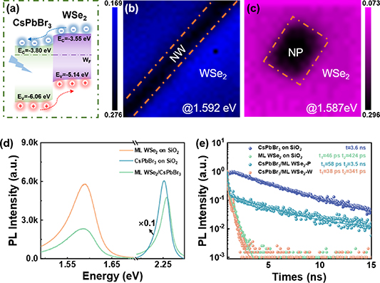
Figure 2. Optical properties of the CsPbBr3/WSe2 heterostructure. (a) Schematic Type-II Band alignments of CsPbBr3/WSe2 from literature, the arrows represent different charge transfer pathways. (b) and (c) PL emission intensity mapping of CsPbBr3 NW/ ML WSe2 at 1.592 eV and CsPbBr3 NP/WSe2 heterostructure at 1.587 eV under 532 nm laser pumping. (d) PL and (e) TRPL spectra comparison of isolated CsPbBr3, isolated ML WSe2, and CsPbBr3 NW/WSe2 heterostructure at room temperature.
Download figure:
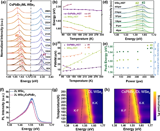
Standard image High-resolution imageThe phonon scattering of the heterostructure is examined by temperature-dependent Raman spectra. Figures 3(a) and (b) compare the Raman spectra of ML WSe2 and CsPbBr3/ML WSe2 heterostructure from 93 to 298 K. The temperature-dependent Raman scattering of WSe2 after heterostructure formation is similar to that of pristine WSe2. The intensity of the WSe2 peak (249 cm−1) decreases during cooling down and the peak position is basically unchanged (see figure 3(d)), which indicates that high temperature growth of CsPbBr3 does not cause damage to the underlying fragile WSe2. In comparison, the Raman scattering of CsPbBr3 is more complex. The Raman scattering of CsPbBr3 is diffuse at room temperature, but increases rapidly and becomes clearer during cooling down. At 213 K, the Raman scattering intensity of CsPbBr3 outweighs that of WSe2. At 93 K, the Raman scattering of CsPbBr3 is so strong that the vibration mode of WSe2 becomes nearly unobservable. At this temperature, CsPbBr3 is an orthorhombic phase and all its Raman modes are active, so the heterostructure shows strong Raman characteristic peaks at 48 cm−1, 65 cm−1, 73 cm−1, 123 cm−1, 152 cm−1 and 306 cm−1 [40] where the peaks at 123 cm−1 and 152 cm−1 are ascribed to the stretching vibrations of Pb–Br, which belong to the transverse optical (TO) phonon and longitudinal optical (LO) phonon, respectively [41, 42]. It is interesting to see that the second order LO vibration mode at 306 cm−1 depicts a similar intensity as LO. For the Raman at low wave numbers of 40–90 cm−1 as shown in the enlarged view in figure 3(c), the vibration modes at 65 cm−1 and 73 cm−1 are related to the vibrations of the [PbBr6]4− octahedron [43]. As the temperature increases to room temperature, the diffuse Raman peaks are consistent with the Raman signature of the cubic phase CsPbBr3 [44]. Meanwhile, the CsPbBr3 on SiO2 was also characterized by XRD (see figure 3(d)). Five characteristic diffraction peaks at 15.56°, 21.99°, 30.70°, 38.32° and 44.60° are clearly observed, which can be assigned as the (100), (110), (200), (211) and (220) crystal planes of the cubic phase CsPbBr3 [45, 46]. The growth of cubic CsPbBr3 is attributed to the high growth temperature [46]. This suggests that a temperature-dependent phase transition may have occurred in CsPbBr3 during the cooling process. This phase transition has been observed in single-crystalline CsPbX3 (X = Cl, Br, I) NPs and CsPbX3 quantum dots [46, 47]. Figures 3(e) and (f) present the variation of the peak position and full-widths at half-maximum (FWHM) of the phonon modes with temperature. The peaks of the LO and 2LO phonon modes are shifted linearly to the high frequency by about 4.5 cm−1 and 1.5 cm−1, respectively, with the change of temperature from 93 K to 298 K. Meanwhile, the FWHM of LO and 2LO increases linearly with temperature.

Figure 3. Temperature-dependent Raman spectra of (a) ML WSe2 and (b) CsPbBr3/ML WSe2 heterostructure. (c) Magnified Raman spectra for the black dotted line region in (b). (d) XRD spectrum of CsPbBr3 on SiO2. Extracted Raman peak positions (e) and (f) FWHM variation during the temperature range from 298 K to 93 K.
Download figure:
Standard image High-resolution imageFurther temperature-dependent PL experiments on the CsPbBr3/ML WSe2 heterostructure are carried out in the range of 298 K–93 K. The intensity of the emission peaks of both CsPbBr3 and WSe2 gradually increases during the cooling process (figure S4). The normalized spectra are shown in figures 4(a)–(c). The emission peaks from CsPbBr3 and WSe2 undergo a blue shift of 8 meV and 70 meV, respectively, and their FWHMs gradually become narrower during cooling down. The surprising phenomenon of the blue shift of CsPbBr3 is consistent for all CsPbBr3 nanocrystals (see figure S5) grown in this work but is in contradiction to the literature reports [48]. Considering the metastable cubic phase as well as smaller emission energy at room temperature, the slightly blue shift of emission during cooling down process may be related to the structural change. For the CsPbBr3 emission, a high-energy peak appears as a shoulder at 2.316 eV when the temperature is below 133 K. During the power-dependent PL at 93 K in figure S6, this shoulder peak remains essentially constant with increasing excitation power, indicating that the peak is not caused by defects. We speculate that this peak may be related to the phase transition of CsPbBr3 during the cooling process, which is similar to the phenomenon occurring in the same type of perovskite [49, 50]. The occurrence of this peak is also in agreement with the above Raman analysis. In addition, WSe2 shows a low-energy peak of about 1.586 eV near the exciton emission peak at temperatures lower than 193 K, which is about 38 meV smaller than the trion emission of the ML WSe2 alone (figure S7), the quality and the thermal treatment for the WSe2 and the ML WSe2/CsPbBr3 heterojunction area is exactly the same. Continuing to cool down to 93 K, the FWHM of this low-energy peak gradually narrows and exceeds the exciton emission intensity (figure 4(b)). Power-dependent PL in figures 4(d) and (e) shows that the peak positions as well as the relative intensity of this low energy peak to exciton emission is nearly independent of the excitation power for over one orders of magnitude. Thus, the emergence of the low energy peak is not likely due to defects. At the same time, according to previous reports, interlayer exciton energy exhibits a power-dependent blue shifts [51]. However, this heterostructure induced low energy emission peak is nearly unshifted during the investigated excitation power range. In addition, after removing CsPbBr3 from the heterostructure with deionized water, the low-energy peaks near WSe2 no longer appeared (figure S8), again confirming that the low-energy emission peak is not due to damage or doping to the WSe2 during the CsPbBr3 growth but induced by the heterostructure itself.
Figure 4. Temperature-dependent normalized PL spectra of (a) CsPbBr3/ML WSe2 heterostructure (HET). Extracted emission peak energies (b) and FWHM (c) from 298 K to 93 K. Power-dependent PL spectra of (d) WSe2 emission peak at 93 K. (e) The peak splitting fitting about (d). (f) PL spectra of isolated DL WSe2, and CsPbBr3 NPs/DL WSe2 heterostructure. Temperature-dependent PL spectra of (g) DL WSe2 (h) CsPbBr3/DL WSe2 heterostructure.
Download figure:
Standard image High-resolution image
In addition to ML WSe2, the optical performance of CsPbBr3/double layer (DL) WSe2 is compared in figure 4(f). After heterostructure formation, the emission of DL WSe2 is nearly unaffected, indicating the effect of charge transfer on photon emission in indirect bandgap WSe2 is not obvious. Reducing the temperature to 93 K, the emission properties between DL WSe2 and the related heterostructure are still similar, showing similar intensity and peak shifts in the K-K and K-F bands. The above-mentioned low-energy emission peak close to the trion of ML WSe2 does not appear in the CsPbBr3/DL WSe2 heterostructure. Therefore, it further confirms that the formation of CsPbBr3/ML WSe2 would alter the carrier recombination paths of pristine WSe2 and the heterojunction can result in a new emission peak at low temperatures.
Our results demonstrate that van der Waals epitaxy is a powerful approach to construct high quality perovskite and TMDC heterostructure. Using CsPbBr3/WSe2 as an example, we show the type-II band alignment, efficient charge transfer process and heterostructure related low energy emission at low temperature. These results demonstrate that this hybrid heterostructure with type-II band alignment shows potential application in self-powered photodetection applications.
4. Conclusions
In summary, we demonstrate van der Waals epitaxy of CsPbBr3 on ML WSe2 with different morphologies, including NPs, NWs, and NCs. The growth of CsPbBr3 is very sensitive to the growth parameters. Temperature is the main factor driving the change of CsPbBr3 morphology. We confirm that the CsPbBr3/ML WSe2 heterostructure forms a type-II band alignment and exhibits ultrafast carrier transfer, leading to a reduction of emission intensity and an acceleration of carrier decay rate. Heterostructure leads to the appearance of a broad emission peak at the low-energy side of the WSe2 emission below 193 K, which is ascribed to the band alignment of the CsPbBr3/ML WSe2 heterostructure. Meanwhile, a high-energy peak appears near the CsPbBr3 emission below 133 K, which may be related to the phase transition of CsPbBr3 from the cubic to the orthorhombic phase. In addition, the lattice dynamics of the heterostructure was further investigated by temperature-dependent Raman spectroscopy. Our findings and results demonstrate that van der Waals construction of CsPbBr3/WSe2 heterostructure with type-II band alignment is of potential application in fabricating of self-powered photodetector with superior performance.
Acknowledgments
This work was supported by the National Natural Science Foundation of China (Grant Nos. 61974166 and 62274184) and the Hunan Provincial Natural Science Foundation of China (Grant No. 2021JJ20080). We thank Prof Lin Zhang for positive discussions and support during the XRD measurements.
Data availability statement
The data that support the findings of this study are available upon reasonable request from the authors.
Supplementary data (0.6 MB PDF)