

Abstract
Heterostructures unconstrained by epitaxy have generated considerable excitement due to the discovery of emergent properties—properties not found in either constituent. Heterostructures enable the surfaces on either side of two-dimensional (2D) layers to be used to systematically investigate phenomena such as superconductivity and magnetism in the 2D limit. The ability to choose constituents facilitates the prediction of emergent properties created by the unusual coordination environments at incommensurate interfaces. There have already been many reviews on heterostructures, focusing on a variety of topics that reflect the diverse interest in this area as well as the potential for new technologies. Hence this review focuses mainly on the synthesis and structural characterization of heterostructures containing transition metal dichalcogenides (TMD). This review only briefly discusses 2D materials and TMD/TMD heterostructure devices and the performances that have been achieved. This review provides a historical context for the rapid development of this field and discusses proposed mechanisms for emergent properties. Up to now, the materials used in heterostructures have mainly been materials with 2D structures, as these compounds can be easily cleaved into ultrathin layers. This review discusses the expansion of heterostructure constituents to include materials that do not have 2D structures. Structural changes and charge redistribution between adjacent (or even more distant) layers are likely to be larger for 3D constituents than with 2D constituents based on known misfit layer compounds. Systematic changes in properties with layer thickness, layer sequences, and the identity of constituents will increase our understanding of emergent properties and how they can be optimized.
Export citation and abstract BibTeX RIS
1. Introduction
For at least the past half century scientists have been curious about how material properties change as thicknesses are reduced to the atomic scale [1–4]. In the era before scanning tunneling microscopies, there were significant challenges in directly determining the thicknesses of samples being studied. Instead, indirect methods such as sheet resistance, absorbance, or shadowing effects were used to infer thicknesses. Researchers reported very early that naturally anisotropic compounds, such as the transition metal dichalcogenides (TMD) or graphite, with easily cleavable van der Waals planes were ideally suited for these investigations [1, 3, 4]. As early as 1966, the 'scotch tape' method of cleaving van der Waals solids and isolating finite layers was reported [1]. As dimensions were reduced towards single layers (figure 1), anomalies in exciton binding energy [2] and systematic changes in superconducting properties [3, 4] were discovered. Although novel properties were reported, the analytical challenges in determining thickness and recognizing large domains of constant thickness prevented researchers from discovering that the anomalous properties of materials such as graphene or MoS2 were intrinsic to single layer thick two-dimensional (2D) planes.
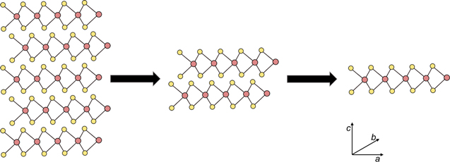
Figure 1. Transition metal dichalcogenides are naturally occurring layered materials with highly anisotropic bonding. Weak van der Waals forces along the c axis enable them to be easily cleaved to obtain monolayer structures, while strong covalent bonds in the ab plane preserve the crystalline structure within a layer during cleaving. The schematic illustrates the structure of five layers (left), two layers (center) and a monolayer (right). The arrows represent the thinning of the sample via cleaving.
Download figure:
Standard image High-resolution imageDuring this same era, Arthur and Choi developed molecular beam epitaxy (MBE) at Bell Labs [5]. The ability to use epitaxial interfaces to grow designed sequences of layers of materials with known thicknesses and structure dramatically increased the repertoire of potentially available functional materials [6]. The ability to imagine sequences of structures that could actually be prepared resulted in increased theoretical activity predicting properties and potential devices from proposed nanoarchitectures. Although the compositional sequences produced by MBE are typically not the thermodynamic ground state of the system, they are often sufficiently kinetically stable at normal operating conditions to be used in devices. Figure 2 shows a schematic energy landscape of kinetically stable heterostructures where the thermodynamic ground state is a physical mixture of the constituents. Just as in MBE, kinetic stability results from sufficiently high inter-diffusion barriers (the energy maxima in the lines connecting the heterostructures with the ground state) that prevent the layers from interdiffusing. Preparation of artificially layered materials with designed nanoarchitectures via MBE has led to fundamental discoveries in physics, including the quantum Hall effect [7]. Control of the nanoarchitecture has provided access to electronic and transport properties not available in the bulk form, and has led to many critical technology-enabling discoveries such as 2D electron gas [8], modulation doping [9], light emitting diodes [10], and quantum cascade lasers [11].

Figure 2. Heterostructures are local minima in the free energy landscape and different stacking arrangements will have different energies. The kinetic barrier to forming the thermodynamic mixture of bulk constituents is a consequence of the activation energy for solid-state diffusion.
Download figure:
Standard image High-resolution imageThe development of MBE was a tremendous advance, but is a technically challenging growth technique. Constituents need to have structures and unit cell parameters with close lattice matches between them for epitaxial growth to occur. If the two constituents do not have a close lattice match, then the interfaces will contain a large concentration of dislocations and other defects necessary to reduce the lattice strain. Besides the lattice match requirement, there are significant challenges associated with finding deposition conditions where material A can be grown on material B and material B can be grown on material A. Finally, the growth of distinct layers at the 2D limit is exceedingly challenging due to mixing that occurs during growth and the competition between completing the first layer and nucleating the next layer.
While MBE research focused mainly on intergrowths of semiconductors with diamond based lattices, other researchers discovered ways to prepare new materials containing intergrowths of constituents with a variety of different structures. In the early 1980s, Koma et al showed that it was possible to grow single layers of compounds containing van der Waals interactions between building units—molecules such as C60, 1D chains such as Se or Te, and/or 2D layers such as the TMD's—on substrates terminated with a van der Waals surface [12, 13]. They demonstrated that the weak van der Waals interaction between constituents drastically relaxed the lattice matching condition usually required in heteroepitaxial growth. The lack of dangling bonds at the van der Waals surfaces resulted in very abrupt interfaces with small defect levels even with lattice mismatches of up to 50% [14]. The removal of epitaxial constraints dramatically increased the number of combinations of constituents that could be utilized in the preparation of heterostructures. 'van der Waals epitaxy' provided the first synthesis route to heterostructures containing ultrathin superconducting, metallic, semiconducting or insulating monolayer dichalcogenides as constituents with controlled and designed nanoarchitecture [12–14].
Van der Waals epitaxy is an innovative technique that allowed preparation of novel heterostructures, however it is still technically very demanding and the challenges of finding growth conditions compatible with growing material A on material B and B on A are similar to those experienced with epitaxial growth techniques. Around this same time period, chemists discovered thermodynamically stable materials, called misfit layer compounds (figure 3), that contained interwoven monolayers of constituents that in the bulk are superconducting, metallic, semiconducting, magnetic or insulating [15]. These compounds are typically prepared directly from the elements at high temperature and single crystals are prepared via vapor transport [16]. The atomic abruptness of the interfaces in misfit layer compounds results from the distinctly different crystal structures of the constituents. Unfortunately, there is essentially no ability to prepare compounds with different constituent layer thicknesses or nanoarchitectures by changing the synthesis conditions [15]. It is also not possible to prepare isolated monolayers or heterostructured bilayers utilizing these high temperature synthesis approaches. The growth of research in the field of 2D materials and novel heterostructures did not accelerate at this time due to the technical challenges of the available growth techniques and the limited analytical tools available to characterize the resulting materials.

Figure 3. Misfit layer compounds are thermodynamically stable heterostructures of alternating layers of rock salt and transition metal dichalcogenide. A defining feature of this class of materials is that they usually possess a single commensurate in-plane lattice parameter.
Download figure:
Standard image High-resolution imageThe activity level in the field of 2D materials has exploded in the last decade fueled by the discovery of novel properties in graphene by Novoselov, Geim and coworkers that resulted in their sharing of the Nobel prize in Physics in 2010 [17–19]. This growth in activity is a consequence of analytical advances (scanning probe microscopy and aberration corrected electron microscopes), the rediscovery of the scotch tape approach to cleave van der Waals compounds, and a breakthrough in the use of optical microscopy to rapidly identify crystals of different thickness [20]. The 'Scotch-tape method', mentioned earlier, is simple, effective and does not require either a large investment or complicated equipment. The optical contrast mechanism of ultrathin layers on a silicon wafer coated with SiO2 is now well understood [21, 22]. This technique permits the rapid scanning of large areas to identify optimal crystals using a light microscope, which is neither expensive nor complicated. The resulting literature on graphene alone is enormous, with estimates of over 10 000 papers a year being published [23]. The second wave of research in this area has focused on related materials whose bulk structure contains strongly bonded layers separated by weak van der Waals forces, including diverse materials such as hexagonal boron nitride [24, 25], TMD [26–32], fluorographene [33], and new elemental analogs of graphene—germanane [34–36], silicone [37], and phosphorene [38, 39]. There are already multiple reviews available on these materials, and the sheer number of papers published makes a comprehensive review daunting. Due to the large amount of literature on the various 2D-materials this review will focus on the emerging field of heterostructures containing dichalcogenide layers. A schematic of various heterostructures is shown in figure 4. Since there are already excellent reviews that focus on emergent properties and devices [40, 41], this review focuses on the synthesis and characterization of heterostructures.
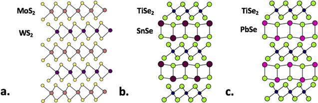
Figure 4. Structural schematics of heterostructures composed of various 2D materials. (a) MoS2 and WS2—yellow represents S, purple represents W and rose represents Mo. The constituent layers are held together by weak van der Waals interactions. (b) SnSe and TiSe2—green represents Se, magenta represents Sn, and blue represents Ti. The SnSe layer does not have a layered structure, but is a fragment of a distorted rock salt structure. (c) PbSe and TiSe2 (green represents Se, blue represents Ti, and maroon markers represent Pb).
Download figure:
Standard image High-resolution imageResearchers have discovered that the properties of monolayer materials depend on the substrate they are attached to, and that the properties can be emergent—i.e. not found in either the monolayer or the substrate [42, 43]. This has spawned investigations into heterostructures containing two or more 2D materials combined into a composite, and there have been considerable efforts made to understand the origin of emergent properties [42–57]. Several origins have been proposed for different emergent properties, including changes in band structure due to removing adjacent layers, finite size effects, structural changes with layer thickness, strain, and the presence of adjacent layers as discussed in the following section. We will also discuss the synthesis and characterization of dichalcogenide containing heterostructures.
2. Origins of emergent properties
In the context of 2D materials, an emergent property is a property that does not exist in a bulk compound, but occurs as the material becomes increasingly thinner. Frequently, the emergent property only occurs when thickness has been reduced to a monolayer [17, 26, 27]. In heterostructures, emergent properties arise when adjacent layers interact with one another. These properties are not present in the individual constituent compounds [58]. Harnessing the power of heterostructure systems for a variety of uses—optoelectronic, thermoelectric, magnetic, etc—depends on developing a set of design principles to understand how to optimize emergent properties. For synthetic groups, the ability to precisely control thicknesses and sequences of layers in a heterostructures is a critical task that is necessary for the systematic study of structure/property relationships. For theoretical groups, identifying the combination of layers and their structural characteristics that give rise to a specific set of properties is a challenge. The need is to inform what parameter spaces and nanoarchitectures must be explored to optimize desirable properties. In the following paragraphs, we discuss the underpinnings behind categories of emergent properties, highlighting the discussion with representative examples.
2.1. Changes in band structure due to removing adjacent layers
Perhaps the most obvious cause for emergent properties in single-layer systems is the removal of electronic interactions between adjacent layers. The loss of orbital overlap changes the band structure and, consequently, gives rise to new properties. Graphene is the prototypic example. Each carbon is sp2 hybridized, leaving the pz orbitals—oriented perpendicular to each hexagonal layer—half empty. In graphite, the pz orbitals in adjacent layers interact to create a filled orbital from the bonding interaction and an empty antibonding orbital. Overlap of these bands causes graphite to be a semimetal. In a single sheet of graphene, this orbital remains half-filled leading to a zero-gap semiconductor with a linear Dirac-like spectrum around the Fermi energy [59], resulting in the emergent properties discovered by Novoselov, Geim and coworkers [17]. The semiconducting dichalcogenides with trigonal prismatic coordination of the transition metal (MoS2, MoSe2, WS2, WSe2) are a second example wherein emergent properties result from a loss of interlayer interactions [26, 27]. In 2010, two independent studies were published that showed MoS2 transitions from an indirect to direct band gap material in going from a bilayer to a monolayer [26, 27]. In 2013, Komsa et al showed that wave functions at the Γ point extend from the chalcogen atoms into the Van der Waals gap, leading to strong interactions with the  orbitals of the transition metal in the adjacent layers (for a 2H polytype) [60]. The highest energy position of the valence band in the bulk is at the Γ point. This band rises in energy due to an antibonding interaction between the layers. In the monolayer, this antibonding interaction is removed, decreasing the energy of this band as it approaches the Γ point, resulting in it being below the energy at the K point. The energy of the conduction band and its general shape do not change significantly with thickness, so the lowest energy point in the conduction band stays at the K point [61, 62]. The net result is that the monolayer has a direct band gap.
Since the impact of changing coordination at interfaces is apparent even in systems with weak van der Waals interactions between layers, more significant changes are observed in heterostructures with constituent layers that are more three dimensional. Constituents that in the bulk have a rock salt structure, for example PbSe, distort significantly when they are present as a bilayer in a heterostructures adjacent to a dichalcogenide. The Pb and Se atoms that are in the same (001) plane in the bulk are puckered in the bilayer, with the Pb and Se planes displaced from one another by over 0.2 Å in (PbSe)1(MoSe2)1 [63]. This distortion results from the termination of the rock salt structure and the interaction between the constituent layers. This has significant consequences for the band structure, but also impacts a range of other properties. An example is the surface segregation of alloys. There is a different chemical composition at the surface of an alloy from that in the bulk [64], because surface energies depend strongly on the crystal structure of the alloy components [65]. Another example is changes in solubility in alloy systems. Sn and Pb are miscible in bilayers of PbSe–SnSe alloys across the entire solid solution, but the bulk phase diagram shows a large miscibility gap [66]. Changes in bonding at interfaces and between constituents at interfaces are likely to become valuable tools used to tune and control properties as they become better understood.
2.2. Finite size effects
As the thickness of a layer is reduced below the de Broglie wavelength of the electron wave function, there is a transition from continuous to discrete energy levels [67]. In 1993, Hicks and Dresselhaus described how changes in the density of states due to localization within a layer could greatly enhance the Seebeck coefficient in heterostructures, specifically calculating potential enhancements in thermoelectric performance for Bi2Te3 containing superlattices [68]. They considered the Bi2Te3 layer as a 2D quantum well with potential barriers formed by the physical boundaries of the layer. The calculated band structures showed sharp features in the density of states that were predicted to enhance the thermoelectric power factor [69]. The emergent properties found in graphene were also initially thought to result from changes in electronic structure due to quantum size effects. The discovery of strong photoluminenescence in TMD and the crossover from an indirect and direct band gap as thickness is reduced to a monolayer initially lead to speculation that quantum size effects might be a general phenomenon in 2D monolayers [26, 27]. Since these initial reports, MX2 monolayers, where M (Mo, W) and X (S, Se), have been found to have other novel excitonic properties, including efficient control of valley and spin occupation by optical helicity [28, 29, 70–73]. Additional studies focused on the fundamental excitonic physics of low-dimensional materials and potential technological applications are being rapidly reported [73–82].
There has also been considerable effort aimed at distinguishing between properties that emerge in ultrathin materials due to unusual features in their band structure (for example, interactions between layers in the bulk) and features that result specifically from the quantization and changes in energy that result from finite size effects [62]. One strategy for attributing particular emergent properties to either of these two effects is to study properties as a function of relative angle between monolayers or between monolayers and substrate. Figure 5 shows a schematic of a rotationally disordered heterostructure. If the phenomena are dominated by a finite thickness phenomena, then the effect of relative rotation angle will be relatively small [83]. If the phenomena are due to interlayer interactions or their removal, then rotation angle will have a pronounced effect [83]. First principle calculations of these systems as a function of rotation angle are challenging, because the size of the supercell varies considerably and is always considerably larger than the primitive unit cell of either a single layer or the stable bulk polymorph. Consequently, atomistic simulations are limited to special twist angles with manageable supercell sizes instead of random orientations. Simpler models that attempt to captures the essential physics are often used. There were extensive studies investigating the properties of bilayers of graphene with rotation angle soon after the novel properties of monolayer graphene were reported, showing that the interlayer interaction changes dramatically as the angle is changed [59, 84–92]. These studies suggest that interlayer interactions, rather than finite size effects, dictate the difference in properties between monolayer and bilayer graphene. Initial studies exploring the effect of rotation angle in bilayers or bilayer heterostructures of Mo and W containing dichalcogenides also show a strong dependence of properties on stacking sequence or rotation angle [83, 93–101]. This supports the conclusion that the lack of interlayer bonding is an important factor in the direct band gap and novel optical properties of monolayers of these compounds [62].
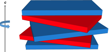
Figure 5. Schematic of rotationally disordered constituent layers within a heterostructures. Lattice mismatch between constituent layers will increase the distribution of rotation angles between layers.
Download figure:
Standard image High-resolution image2.3. Structural changes with layer thickness
As suggested in section 2.1, the most salient feature of monolayers relative to their bulk counterparts is the removal of the electronic interaction between adjacent layers. For very anisotropic compounds—those with strong bonding within layers and weak van der Waals interactions between layers—the structure of free monolayers has been calculated or assumed to be quite similar to constituent monolayers in the corresponding bulk solid [102, 103], in agreement with many transition electron microscopy images [104–107]. For less anisotropic bulk solids, however, more extensive structural changes might be expected at lower dimensions due to the increased influence of surface energy that results from the removal of adjacent layers. In an infinite crystal, the forces exerted by all the other atoms in the crystal determine the position of each individual atom. At a surface, these forces are altered, and surface atoms experience more asymmetric inter-atomic forces. Consequently, the positions of the surface atoms change from the equilibrium in the bulk, assuming distinct spacing and/or symmetry. Indeed, surface reconstructions are a common feature of crystalline solids, with specific distortions depending on the crystal face and atoms at the surface [108]. Surface reconstructions can extend into the bulk, with the extent of distortion decreasing as distance from the surface increases. Hence, structural distortions might be expected to change as a function of layer thickness, due to the relative importance of surface and volume free energies.
There is limited data available on the atomic structure of 2D layers, as most analytical techniques give only information about the symmetry of the layer or perhaps only one or two of the three atomic coordinates of the atoms in the 2D layer. Raman and other optical spectroscopies provide information about changes in symmetry and the stacking sequences of layers (i.e. polytypism) [109]. A review article was recently written that describes the evolution in Raman modes and lattice vibrations in monolayer, few-layer, and bulk systems [110]. Transmission electron microscopy and scanning probe microscopies provide low resolution information about the in-plane coordinates of the atoms in 2D layers. In-plane x-ray diffraction provides information about symmetry and the in-plane lattice parameters. The intensities can be used to refine the in plane atomic coordinates if the data is of high enough quality [111]. Partially due to the challenges in obtaining quantitative information about the structure, the majority of studies on mono- and few-layer anisotropic compounds that can be prepared using the 'scotch tape' synthesis approach have assumed that the bulk structure is preserved in the monolayer. There are a few studies of heterostructures containing 3D solids. There is a report of the structure of PbSe layers, which has a cubic rock salt structure in the bulk, as a function of thickness. A bilayer orientated with the (100) planes is the thinnest layer reported, and it has a square in plane lattice but each of the (100) planes distort such that the Pb atoms sit in a plane extending slightly into the van der Waals gap, and the Se atoms are in a plane slightly interior [112]. This puckering distortion is significant, on the order of 0.2 Å. As the PbSe layer is increased, the magnitude of this puckering distortion decreases. The structure of a four-plane PbSe layer distorts to form two bilayers, with a larger distance between the bilayers. The structure of a six-plane PbSe layer distorts to form three bilayers, with the distortion in the center bilayer different than the outer bilayers. By the time the PbSe layer reaches ten planes, the structure looks like the bulk structure with a surface distortion. This puckering phenomenon and its comparison to the bulk PbSe structure (a) is depicted in figure 6. It was suggested that these distortions result from the interplay between surface and volume free energies [112].
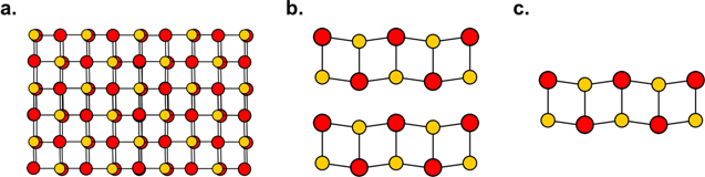
Figure 6. As rock salt bulk compounds are reduced to ultrathin dimensions, the lattice becomes increasingly 'puckered' such that metal cations extend into the van der Waals gap while the chalcogen atoms occupy atomic positions on the interior of the bilayer. (a) The bulk rock salt crystal structure. (b) Two stacked bilayers of a puckered rock salt structured constituent. (c) Structure of a single puckered 2D rock salt bilayer. The metal atoms are shown in red and the chalcogen atoms are shown in yellow.
Download figure:
Standard image High-resolution imageSimilar changes in structure with thickness were reported for SnSe layers sandwiched between dichalcogenide layers [113–118]. Bulk SnSe possess an orthorhombic unit cell. However, a bilayer of SnSe was found to have a square basal plane when interleaved between either MoSe2 or TaSe2 layers [113, 114]. Interestingly, the SnSe lattice was found to have a rectangular basal plane when interleaved with NbSe2 [115], showing the importance of adjacent layers. The in-plane lattice parameters in this heterostructure became increasingly different as the thickness of the SnSe layer increased [116]. Around 40 planes of SnSe are required before the lattice parameters resemble the bulk compound. Similar changes in structure are anticipated as other 3D solids are prepared as 2D layers. The changes in the structure of 2D layers of 3D solids with thickness reflects the changes in the bonding at the internal surfaces, which provides an additional mechanism to tune properties. The unique environment between 2D layers may also make it possible to prepare structures as 2D layers that are not stable as 3D solids [117, 118].
2.4. Strain
Strain has historically been a valuable tool used in semiconductor technology to optimize properties and performance in today's microelectronics devices [119]. In traditional semiconductor devices, strain is typically created during epitaxial growth through lattice mismatch at interfaces. For fundamental studies of strain, external forces can be applied in a variety of ways to plastically deform the material in question. These studies have a long history, with the first report of strain-enhanced mobility in n and p type bulk Si and Ge occurring in 1954 [120]. Many papers have explored the effect of strain on bulk materials, thin films, and epitaxially grown layers, including superlattices [121, 122]. It is not surprising that soon after the discovery of the remarkable properties of graphene, strain was theoretically and experimentally explored as a tool to modify properties [123]. The effect of strain on graphene has been recently reviewed [123].
Researchers have explored the effect of strain on properties of novel 2D materials using various approaches [60, 123–126]. Theoretically changing the lattice parameters is relatively easy, and it is common, for example, to create supercells with varying degrees of strain to approximate rotational angles between layers. As Komsa and Krasheninnikov have pointed out, however, it is difficult to distinguish which features originate from the monolayer or stacking of the monolayers and which are due to the strain artificially introduced into the system to make the calculations easier [60]. Experimentally straining graphene and other 2D materials is challenging because the weak interlayer van der Waal forces that make these materials cleavable and chemically stable as monolayers also make them resilient to deformations induced by epitaxy. Indeed, dichalcogenide heterostructures epitaxially grown by Koma and coworkers [124] and epitaxial growth of TMD mono-layers on grapheme [125] both resulted in layers with lattice constants very close to those of the bulk and the isolated monolayers. This is a consequence of the energy cost for straining the lattice and exceeding the incremental bonding energy between layers. van der Waal forces are significantly weaker than the covalent bonds found at the interfaces of epitaxial III–V heterostructures. The weak interlayer bonding in van der Waals heterostructures does not provide a sufficient energy barrier to trap growing layers in their strained state during growth [60].
Researchers have been clever in using a variety of approaches to strain 2D monolayers, and the large volume of research published in this area has recently been reviewed [126]. Monolayers have been placed on substrates that have different thermal expansion coefficients, resulting in increasing strain as a function of temperature. 2D materials have also been placed on flexible substrates, which, when bent create a tensile strain on the top of the substrate and a compressive strain on the bottom. This strain can also arise if a 2D material is placed on an elastic substrate. Compressive stress is created if the substrate is elongated before the 2D material is applied, while tensile strain occurs if the 2D layer is placed on the substrate and is subsequently elongated. In a similar manner, the piezoelectric effect can be used to stretch or compress a 2D layer on top of a suitable substrate. The van der Waals bonding between the monolayer and a substrate can maintain approximately 1% strain before releasing. A monolayer can be tacked in place by an edge coating of metal, increasing the magnitude of achievable strain. Releasing strain on a monolayer can produce layers with controlled wrinkling. This is typically accomplished by positioning a 2D layer on a stretched substrate and then releasing the tensile strain on the substrate. Micro Raman spectroscopy is a valuable tool to investigate local strain in 2D materials and heterostructures and this technique will be discussed in more detail later in this review [127–129]. Strain will continue to be a valuable tool in the pursuit to tune the properties of monolayers to both understand fundamental interactions and create devices.
2.5. The presence of adjacent layers
Monolayers may be thought of as one-dimensional 'particle in a box' situations, with the electrons of the layer confined to that layer. Because the potential barriers at the walls of the box are not infinite, the wave functions extend outside of the box for a couple of angstroms, decaying exponentially. These extended wave functions interact with adjacent layers or surfaces causing the layer properties to be modified [42]. This interaction with adjacent layers can significantly modify the band structures of the individual 2D layer, even though no real chemical bonds are formed between them [43]. The resulting properties of the 2D layer depends on the alignment of bands between that 2D layer and the substrate, the density of states of each material, and the extent of charge transfer due to electrons having different chemical potentials in the various constituents. In semiconducting 2D layers, for example, the exciton binding energy and the quasiparticle band gap are influenced by the choice of substrate material and also by excited electrons within the 2D layer [44–47]. When a semiconducting single layer TMD is placed on a metallic substrate, a strong band gap renormalization is observed [48, 49]. Interactions between monolayers and a substrate can be strong enough to modulate electronic properties even if the interface is not epitaxial [50, 51]. The number of papers describing different behaviors of monolayers on various substrates is rapidly expanding and researchers are investigating a wide range of monolayers and substrates both theoretically and experimentally [52–57]. Theoretical predictions about non-lattice matched monolayers are complicated by the large unit cells required to avoid introducing significant strain into the constituents and by the difficulties in treating the van der Waals interactions and charge transfer at interfaces [60, 130]. Experimentally, applying a gate voltage to a substrate or changing the Fermi level by chemical doping are both being used to discover new phenomena in 2D monolayers [131, 132]. The dependence of properties of monolayers on changes in chemical potential provide a mechanism to create novel sensors [133, 134].
3. Heterostructures containing TMD
Adding an additional layer (or layers) on top of a monolayer on a substrate, creating a three-component sandwich, produces additional complexity. Since many potential devices will use monolayers that are buried as part of an overall architecture, research in this area will expand considerably as the ease of both manipulating monolayers and directly growing different monolayers on top of one another increases. We will refer to these composites as heterostructures, and heterostructures of TMD are the topic of the rest of this review article.
Heterostructures will grow in importance as a research field for a variety of significant reasons. First, devices will require additional layers (top and bottom) to provide electrical contacts, protect the monolayers from damage, and to generate emergent properties through the interaction between layers. By judiciously choosing adjacent top and bottom layers, existing properties can be modified and novel properties can be created. The ability to predict the structures and properties of heterostructures that have not yet been created provides an opportunity for theorists to create models to probe for unique effects in systems that have not been experimentally prepared [135]. These predictions will provide significant motivation to prepare the identified systems. The resulting differences in properties from those predicted and their dependence on nanoarchitecture will lead to a greater understanding of structure-property relationships.
There is already an impressive number of papers that describe the properties of heterostructures containing graphene [55, 136–158], and a growing number of papers that describe heterostructures containing one or more dichalcogenide and the properties that arise from the interaction between constituents [159–162]. In the future, new constituent layers will be prepared and assembled with control of both thickness and the sequence of layers. Researchers will have a set of building blocks to create new materials where the nanoarchitecture and resulting interaction between constituents provide the tools to discover novel and optimize known properties. Perhaps, much like a building is designed using optimally designed composites of concrete and steel, new materials will be designed by creating nanocomposites with specific architectures to optimize emergent properties for targeted applications. This will require the development of an understanding of how emergent properties of 2D layers arise and how 2D layers interact to form composites that outperform individual materials.
3.1. Synthesis
Due to their promising applications in a wide variety of devices [163], researchers have devoted considerable effort to discovering efficient means of synthesizing monolayers and heterostructures, with ongoing efforts aimed at producing uniform structures over large areas. The 'scotch tape' method enables the preparation of heterostructures composed of different monolayers, but the micromechanical manipulations require considerable skill and patience. There are also concerns about surface contamination that can affect the properties of the resulting heterostructures and the technique is limited to constituents that can be isolated and stabilized as monolayers [137, 141, 164, 165]. However, micromechanical exfoliation is a surprisingly robust approach and there are many reports of new combinations of constituents and novel device structures being prepared using this technique.
While most of the initial work has been based on monolayers cleaved from single crystal materials, there has been substantial interest in developing approaches that provide monolayers over sizeable areas. A number of TMD have been prepared on a variety of substrates using chemical vapor deposition, sputtering and other vacuum deposition approaches where the chemical fluxes and substrate temperatures are controlled to grow a defined number of layers of a desired material [166–171]. When the layers are parallel to the substrate, the challenge in these growth techniques is controlling the conditions to completely grow each layer before nucleating the following layer. This challenge arises from the limited number of variables that can be easily controlled, including the mass flow of reactants and temperature profiles. The synthesis of vertically oriented layers, needed for catalytically active samples, is more challenging, typically requiring a template layer [172, 173]. The nucleation and growth issue is addressed by Koma's van der Waals epitaxy growth technique [12–14], which has grown in use all over the world. A wide variety of new systems prepared using this approach are reported every year [138, 171, 174–179]. The in situ monitoring of growth using low energy electron diffraction enables the growth conditions to be systematically optimized, but achieving layer-by-layer growth is challenging. A third approach to prepare a defined number of layers is to deposit a limited amount of the metal and then react this metal layer at low temperatures with chalcogen containing reactants. Both ALD [136, 180–182] and physical deposition approaches [183] have been used to deposit a defined amounts of metal, however, confirming that exactly a monolayer has been deposited is challenging. In a related approach, it has been shown that exchange reactions can be used to change oxide films into chalcogenide films while preserving the structure and thickness of the original film [184].
In parallel with these layer-by-layer vacuum based growth techniques discussed briefly above, there has been a significant effort to develop low cost solution processing approaches to 2D materials [140, 184–191]. Many compounds with layered structures can be exfoliated in solutions using a variety of approaches (ion intercalation, ion exchange, sonication) as summarized in several reviews [192–194]. The key to exfoliation is finding a combination of solvent and starting layered material such that the interaction of the layers and ions within the solvent is larger than the interaction between the layers of the starting layered material. For neutral systems such as graphene, the solvent-graphene interaction needs to be large to compensate for the loss of bonding between the graphene layers. For starting materials containing ions, the enthalpy of solvation of the cations needs to overcome the bonding between layers and the entropy loss associated with organizing solvent molecules around the ions. Exfoliated layered materials, which have been used for centuries in a variety of applications, continue to grow in importance. Researchers have discovered applications ranging from catalysts and sensors, which take advantage of both unusual properties and large surface areas [187], to polymer-exfoliated clay composites used as gas diffusion barriers [195]. Assembly of the 2D sheets created by exfoliation into heterostructures range from a sheet-by-sheet assembly of specific stacking sequences to self-assembly of sequences from solutions [186]. Groups are beginning to use liquid phase printing and spin coating techniques to make simple devices from solution precursors [139]. The scalability of solution processing and its low intrinsic cost relative to vacuum processing approaches gives solution processing a unique niche that will continue to expand.
The challenges involved in the synthesis of heterostructures with targeted nanoarchitecture are different than those in the traditional synthesis of new alloys or compounds. Since most targeted heterostructures will be metastable, the traditional high temperature or fluid phase mediated synthesis approaches that mostly yield thermodynamic products will not work. It has been recognized that approaches that control kinetics and reaction intermediates, such as MBE, are required. A number of interesting approaches to dichalcogenide-containing heterostructures are being developed that rely on preparing a precursor containing some of the structure of the targeted heterostructure, which is then further processed using approaches that preserve the structure of the precursor (figure 7) [66, 183, 196–201]. The appeal of these approaches is that they avoid the challenges of finding suitable growth conditions as needed for van der Waals epitaxy, so several different constituents can be prepared on top of one another (i.e. A on B or C, B on A or C, and C on A or B) which is required to prepare complex layer sequences with multiple constituents. Encouragingly, theory groups are beginning to explore the growth process, which can provide insights into why some approaches work and also potential new approaches to try [202, 203].
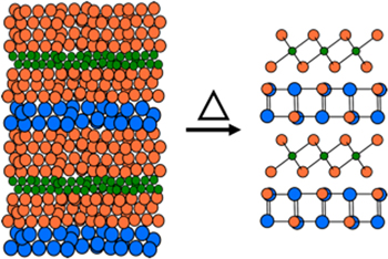
Figure 7. Synthesis of metastable heterostructures from a precursor with defined amounts of elements deposited. The precursor is annealed at low temperatures to self assemble the desired heterostructure.
Download figure:
Standard image High-resolution imageThe fundamental underpinning of the post processing of designed precursors is surprisingly similar to that involved in traditional organic synthesis. In both cases precursors are designed and then reacted to obtain desired products, with the reaction conditions and or design of the precursor used to favor the formation of targeted products. Diffusion constraints (temperature and/or protecting groups) are used to direct the system towards desired products. The concept of energy landscapes [204] provides a valuable framework to potentially understand how the structure of the precursor and/or the reaction conditions enables the synthesis of metastable heterostructures [205].
3.2. Characterization
Characterizing the structure of constituent layers within heterostructures is critical, as most emergent properties will be intimately connected with structural changes at the interfaces or throughout the thin layers. These structural changes may be due to the large surface to volume ratios in the individual constituents and/or due to interactions between the constituents. Understanding the interplay between synthesis conditions and the structure as well as the density of defects present in the heterostructures is very important, and it is limited by the ability to characterize the samples. Characterizing even the average structure of a 2D monolayers or heterostructures is, however, a major challenge due to the small amounts of material present. Determining parameters such as local and average layer thickness, bond lengths and average composition are significant analytical challenges. The development of new analytical tools, for example the easily observed optical interference pattern differences between graphene and SiO2 as a function of the number of layers [21, 22], has been and will continue to be critical as this field advances. Numerous techniques have already been used to determine different structural features of heterostructures as discussed in the following paragraphs.
Measuring thickness of layers, both locally and over larger areas, has been a known challenge in this field. Historically, thickness was estimated through resistivity [4] or electron microscopy measurements [1]. In the resistivity measurements, researchers assumed a constant resistivity and used the resistance per square to determine thickness [4]. The electron microscopy experiments used both cross sections and the extent of shadowing to measure thickness [1]. Both optical interference [21, 22] and scanning tunneling microscopy measurements were critical new tools used by Geim [19] and Novoselov [18] to determine the thickness of different regions as they probed the properties of graphene as a function of layer thickness. Additional tools need to be developed to speed the selection of heterostructured samples and preparation conditions.
Several different x-ray techniques have been used to determine the thickness and structure of thin film samples. X-ray reflectivity (XRR), an in-FAB metrology tool in the semiconductor industry, is very sensitive approach to measuring thickness [206]. Figure 8 shows a calculated reflectivity pattern (middle blue trace) for a heterostructure containing 8 MoSe2 trilayers and two experimental attempts to prepare an 8 layer MoSe2 film. The XRR pattern represents the sum of the intensities gathered over a relatively large, cm2 sample area. The top pattern clearly deviates from that calculated for the ideal sample, with the low angle portion of the scan, which is dominated by front surface and back surface interference, having a different period than the higher angle portion of the scan (10°–13°), which is dominated by the incomplete destructive interference of the MoSe2 trilayers. This suggests that while the sample contains regions with the targeted 8 trilayers of MoSe2, other regions are thinner than targeted. The bottom experimental pattern closely resembles the calculated pattern, indicating that the majority of the sample contains the targeted 8 trilayers. One challenge in interpreting XRR data remains determining which interfaces in a sample dominate the intensity pattern. Ellipsometry is a complementary tool that can be used to determine film thickness. Extracting thicknesses from ellipsometry data requires assumptions about the index of refraction at the wavelengths used. Resonant x-ray reflectometry (RXRR) is a developing tool that is, in principle, capable of determining complex chemical composition profiles in a non-destructive manner, as data collected at different energies greatly constrains potential structures [207]. A challenge in extracting detailed, quantitative information from XRR, elipsometry and RXRR data is the needed to construct models. While software exists to optimize models to fit experimental data, it is possible for incorrect models to do reasonably well in fitting limited data sets, so complementary information from other analytical techniques that can be used to develop initial models is very valuable.
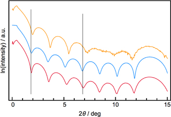
Figure 8. Calculated (blue) and experimental (red and yellow) XRR patterns for MoSe2 films containing 8 layers.
Download figure:
Standard image High-resolution imageFor heterostructures containing more than one repeating layer sequence, specular x-ray diffraction provides a convenient tool to quantitatively determine the average position of atomic planes within the repeating layer sequence. There are relatively few examples in the literature where specular x-ray diffraciotn and subsequent refinement are used to determine the location of atomic planes [208–210]. Figure 9 contains the specular diffraction pattern of (PbSe)1(VSe2)1 along with a calculated pattern and the difference between them, where Rietveld refinement was used to optimze a model for the structure. The optimized structure is shown in the inset of figure 9, with the inter plane distances from the model graphically displayed by the layer seperation. Due to the alignment of constiuents parallel to the substate, only the c-lattice parameter can be extrated from the specular diffraction pattern and the refinement provides the location of the individual planes of atoms in the c-direction. From the arbitrary locations of the atomic planes, the interplanar distances can be determined and any deviations from the bulk structure will be observed. From this model the V–Se intra unit distance was found to be 0.151 nm and places the V plane of atoms symetrically between the two Se layers [63]. The metal layer in the dichalcogenide might not always be centered, however, as asymetric heterostructures might cause planes of atoms to shift due to the forces caused by the presence of different neighboring layers. In the PbSe consituent, there is a disortion of the rock salt layer due to the termination of the rock salt structure and the attraction and repulsion of the cations and anions respectively to the neighboring dichalcogenide layers. The distance between the VSe2 and PbSe layers was calculated to be 0.331 nm, which is longer than the van der Waal's gaps in pure dichalcogenides, presumably due to the layers having incommensurate structures [63]. The use of Rietveld refinement with models informed by complimentary techniques allows for fairly accurate determination of constituent layer crystal structures within layered materials.

Figure 9. Locked-coupled theta-2theta x-ray diffraction used to understand the structure of a PbSe–VSe2 heterostructure. A Rietveld refinement was conducted to optimize the structure to understand where planes of atoms are located. The inset shows a schematic of the structure of the compound with parameters that can be determined using Rietveld refinement.
Download figure:
Standard image High-resolution imageIn-plane diffraction patterns can be used to obtain the in-plane symmetry and lattice parameters as well as additional information about the basal plane structure of the film's constituents. Figure 10 contains the in-plane diffraction patterns of a 4-layer, 8-layer, and 24-layer MoSe2 film. The reflections in the patterns can be indexed assuming a hexagonal unit cell and the indices are shown on top of each diffraction maximum. Since all expected (hk0) reflections are observed with the anticipated relative intensities, the sample consists of randomly oriented domains within the large (cm2) analytical area. The change in intensity of the reflections between patterns correlates to the difference of the thickness of material in the beam. If the sample were to contain only a single orientation, then rotating the film would result in a set of maxima corresponding to the symmetry of the crystal system—i.e. a 'pole figure' scan. If there is a second constituent in the heterostructures, the in-plane diffraction pattern would contain additional reflections, as shown in figure 11 for a SnSe–NbSe2–MoSe2 heterostructure. The observation of all expected (hk0) reflections again indicates that the sample consists of domains of all orientations.
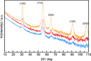
Figure 10. In-plane diffraction of MoSe2 films with 4, 8, and 24 layers (blue, red, and yellow, respectively). All maxima can be indexed as (hk0) reflections of hexagonal MoSe2 to determine the basal plane lattice parameter.
Download figure:
Standard image High-resolution image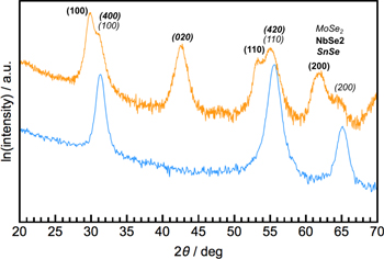
Figure 11. The in-plane diffraction pattern of a 24-layer MoSe2 film is shown in blue. The yellow pattern is an in-plane scan of a MoSe2–SnSe–NbSe2 heterostructure. The additional maxima can be indexed as SnSe and NbSe2 reflections, enabling the lattice parameters of all three constituent structures to be determined.
Download figure:
Standard image High-resolution imageReciprocal space maps can be used to elucidate the extent of interlayer ordering. Figure 12 shows the reciprocal space map of (PbSe)1(VSe2)1 [63]. In this map, there are no distinct (hkl) reflections expected from the super lattice. Only broad maxima from the PbSe and VSe2 are observed. This is consistent with extensive, random rotational disorder between constituents. Rotational disorder is not surprising in heterostructures due to the strong in-plane bonding in constituent layers. Even when one system is chemically 'soft' due to a more three-dimensional structure, such as the SnSe containing heterostructures shown in the diffraction figures, the small energy difference between different stacking configurations and the kinetically controlled synthesis approaches used to make them will both likely prevent the system from finding a distinct, low energy, long range stacking arrangement. The rotational disorder and resultant lack of (hkl) diffraction maxima limits the ability to determine average bond lengths both within and between constituent layers.
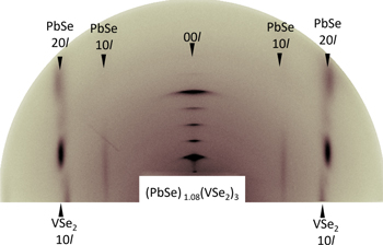
Figure 12. Reciprocal space map of a PbSe VSe2 heterostructure. For both PbSe and VSe2 there are no distinct reflections that correspond to the super-lattice period, only streaking indicating extensive rotational disorder between constituents.
Download figure:
Standard image High-resolution imageTransmission electron microscopy has been an indispensable tool for obtaining structural information about constituent layers and the relative orientation between them [20, 111, 211–216]. For example, plan view HAADF-STEM images of monolayer MoS2 show that the molybdenum and sulfur atoms are arranged in a hexagonal configuration with Mo–S and Mo–Mo separations of ∼0.19 and ∼0.33 nm respectively [211]. This is consistent, within error, to the bulk structure which contains Mo trigonal prismatically coordinated by S [211]. Cross section HAADF-STEM images also corroborated trigonal prismatic coordination of Mo by S. Cross section HAADF-STEM images of all six possible heterostructure isomers containing 4 bilayers of SnSe and 4 MoSe2 trilayers in the repeating unit showed that the Mo is trigonal prismatically coordinated by Se, but that there was extensive rotational disorder between adjacent MoSe2 layers and between MoSe2 and SnSe layers [212]. A schematic illustration of these isomers is shown in figure 13. It is also possible to use HAADF-STEM images to obtain the average separation between atomic planes as demonstrated by Mitchison et al [111]. The interplanar distances from these experiments can be used to create initial models for Rietveld analysis of x-ray diffraction data. The location of specific atoms within monolayers and the distribution of elements between layers in heterostructures can be determined using HAADF-STEM contrast or EDX-STEM data [213, 214]. These examples demonstrate how various STEM analytical techniques provide direct structural information. This insight is valuable for heterostructures both at a local level and to provide structural models for the interpretation of more global analysis techniques. Determining fine scale information, such as interlayer and interatomic distances, will become increasingly important to explain changes in properties.
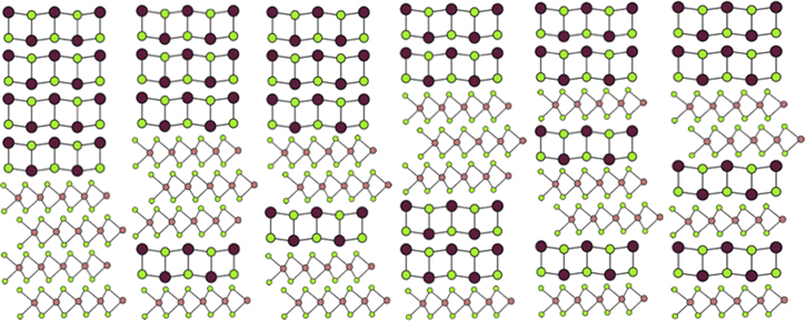
Figure 13. Schematic illustrations of the 6 possible sequences of layers requiring 4 dichalcogenide and 4 rock salt bilayers without repeating a portion of the sequence. Repeating one layer of each structure 4 times or two layers of each structure twice create an eight layer repeat pattern with four layers of each structure, but segments are repeated.
Download figure:
Standard image High-resolution imageScanning probe techniques offer another route to determine the structural arrangement of atoms in both monolayers and the top layers of heterostructures [217–220]. A particularly valuable use of scanning tunneling microscopy/spectroscopy has been to examine the effect of synthesis parameters on the structure and defect levels of the resulting samples [217]. Scanning probe microscopy provides the ability to map electronic states and correlate them to topographical features and specific arrangement of surface atoms [218]. Probing changes to surface structure and electronic states as a function of exposure to atmosphere or different gases is particularly important to understanding the differences in properties of samples prepared in various environments [219]. Scanning probe microscopy is a critical tool to determine changes in thickness of layers transferred using the scotch tape approach.
Measuring composition is a significant challenge in heterostructures due to the small amount of material, small probe sizes, and resulting small analytical volumes present in many common approaches. Electron or ion beam techniques are particularly challenging due to the small analytical volumes of the probe beam in the layer of interest relative to the analytical volume buried in the substrate. While the substrate signal can be reduced by changing the accelerating energy of the beam, this also affects the excitation probabilities for different transitions in the layer being probed. Energy dispersive spectroscopic techniques suffer from the need to subtract relatively large background signals, whereas wavelength dispersive spectroscopic techniques (WDS) have a significantly smaller background signal. This makes WDS more appropriate for trace element analysis. Instrumentation improvements are required to increase the signal level necessary to obtain both relative composition and absolute quantitative amounts. Ion beam approaches, such as time of flight secondary ion mass spectroscopy, have the sensitivity to detect monolayers, but rigorously quantifying the ion yields has also proven difficult [221]. For large area samples, techniques such as x-ray fluorescence might provide enough signals, due to the increased area probed, to quantify the extent of fractional layers, but quantifying the geometric factors affecting the signal is challenging. Atom probe tomography is another approach to determine both composition and structure, and has been shown to be particularly useful to determine local occupancies of dopant atoms in 2D heterostructures [222].
Raman spectroscopy is the most common analytical tool used to probe 2D materials [109, 223–228], because characteristic vibrational modes can be used to identify specific monolayer materials and polytypes [229]. It is a quick, non-destructive probe of small areas and does not require complicated sample preparation. The high-frequency intralayer vibrational modes of different dichalcogenides each have characteristic frequencies. These high frequency interlayer modes do not shift much in energy or intensity from the bulk dichalcogenide with the same local coordination of the transition metal (octahedral or trigonal prismatic) [229]. The low-frequency breathing and shear modes, however are different for each polytype [109]. Once vibrational modes for different materials are tabulated, the Raman spectra of monolayer samples can be used to determine the local coordination and stacking motif of the layers. In few layer dichalcogenides and in heterostructures stacks, the changes in local symmetry due to the limited number of layers results in new Raman active modes [230]. For heterostructures or multilayer samples where the layers are not rotationally aligned, the interlayer breathing and shear modes can be highly sensitive to variation of the twist angle [231]. This complicates the Raman analysis of heterostructures and multilayers with random twist angles, and complementary techniques that more directly probe structure, such as electron or scanning probe microscopies, are frequently used in parallel.
Raman spectroscopy has become one of the first tools used for probing the properties of layered dichalcogenides and therefore has been the subject of multiple reviews. We refer interested readers to these excellent reviews. Zhang et al has discussed changes in Raman of TMD as a function of thickness, from monolayer to bulk [110]. A review by Saito et al covers the fundamentals of the polarization dependence of the Raman intensity and the Raman tensor. Zhang et al provide a more comprehensive review of different types of layered chalcogenides [232]. They demonstrate how low frequency modes can be used to probe the rotational angle between layers in a bilayer and to investigate the interlayer coupling of vertically stacked dichalcogenides in heterostructures [229]. Puretzky et al beautifully illustrate this point, using complementary electron microscopy data to demonstrate how low frequency Raman modes due to interlayer vibrations serve as fingerprints to characterize the number of layers and their stacking configurations [233]. These papers and the references they contain provide valuable insight into the importance of Raman spectroscopy as a quick initial probe of heterostructures.
4. Properties
An iterative relationship between theory and experimental probing of physical properties, particularly in the nascent stages of discovery, greatly accelerates advancing a field. Optimizing the properties of dichalcogenide-based heterostructures through rational design is in an early stage and the number of potential heterostructures is enormous even if confined to those containing dichalcogenides [214]. The more theory can be informed by experimental data and vice versa, the faster progress there will be in predicting and engineering the properties of particular heterostructures.
An advantage of TMD as constituents of heterostructures is the wide range of properties that are known in the bulk compounds. Layered dichalcogenides can be metallic, superconducting, semiconducting, semimetallic, catalytically useful, and potential photocatalysts. A wide range of 2D magnetic properties can be found in closely related MPX3 compounds where a phosphorus dimer substitutes for a transition metal in the hexagonal metal layer [234–244]. TMD containing heterostructures provide an entirely new set of parameters, including but not limited to—modulation doping via charge transfer between constituents, layer specific alloying, stacking sequence, rotation angle, and non-periodic graded structures—to combine, tune and/or optimize properties. Relative to more traditional tetrahedral semiconductor-based layered architectures, the chalcogenide surface layers of dichalcogenides provide the ability to abruptly change both structure and composition. The lack of covalent bonding between layers allows for a range of rotation angles between the constituent layers and for their structures to be independent of one another. This field is just beginning and the following sections review recent progress with the discussion grouped around common properties of materials.
4.1. Semiconducting heterostructures
Emergent phenomena in dichalcogenide monolayers were first discovered in semiconducting group 6b (Mo, W) dichalcogenides. MoS2 [26, 27], MoSe2 [70], WS2 [245], and WSe2 [31] have all been reported to transition from an indirect to a direct band gap as thickness is reduced to a single monolayer. Since monolayers of these compounds are relatively easy to isolate and are stable in ambient conditions, these systems and their emergent properties have proven amenable to extensive investigation. The group 6b dichalcogenides all contain a central plane of trigonal prismatically coordinated transition metal atoms, while the tin atoms of the semiconducting SnS2 and SnSe2 compounds, which adopt TMD-like layered structures, are all octahedrally coordinated. It is interesting to note that bulk tin dichalcogenides, like the group 6b analogs, are indirect band gap semiconductors, yet at the monolayer limit, tin dichalcogenides have both been reported to maintain the indirect band gap [246].
In heterostructures containing these and other semiconducting dichalcogenides, the band alignment between the constituents is critically important in determining properties (see figure 14). In so-called type I band alignment, the band gap of one material falls entirely within the bandgap of the other material. In type II band alignment, the two band gaps are offset from each other such that EVB,1 < EVB,2 < ECB,1 and ECB,1 < ECB,2. In type III ('broken') band alignment, the band gap of one material falls entirely within the valence band of the other material. The first reference to heterostructures of semiconducting dichalcogenides found in the literature was on SnS2/SnSe2/SnS2 heterostructures published in 1999. Van der Waals epitaxy [12] was used to prepared these heterostructures and a series of measurements were done to determine band offsets [247]. The recent interest in 2D materials has resulted in several papers reporting band offsets of heterostructures as a function of twist angle between bilayers [93], and between different dichalcogenides that are stacked on top of one another [248, 249]. There has also been considerable interest in lateral heterostructures—i.e. the in-plane junction of two different dichalcogenides [250]. Both calculations and scanning tunneling experiments examining lateral 2D heterostructures have been reported [157, 251].
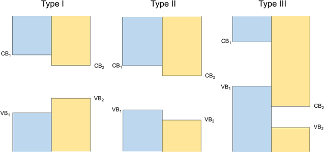
Figure 14. Band alignments in semiconducting heterostructures fall into one of the three categories depicted. In type I heterostructures, the band gap of one material falls entirely within the band gap of the other material. In type II heterostructures, the two band gaps are staggered such that CB2 < CB1 and VB2 < VB1 < CB2. In type III, the band gap of one material falls entirely within the valence band of the other material.
Download figure:
Standard image High-resolution imageThe band alignment has an important influence on the carrier dynamics of electron–hole pairs created when light is absorbed (i.e. 'excitons'). If a heterostructure has type II alignment, for example, the electron–hole pair created by the absorption of a photon in one layer can reduce its energy by transferring either the electron or hole to the adjacent constituent. In MoS2–WS2 heterostructures the holes can substantially reduce their energy by transferring from the MoS2 to WS2 and vice versa for electrons [252, 253]. Significantly, the transfer of the hole between layers does not depend on the orientation of the layers, so epitaxy is not required, and this result implies that lattice mismatch should not affect the transfer rate [253]. This has been confirmed by subsequent reports showing ultrafast charge transfer in MoS2–WSe2 [254], MoTe2–MoS2 [255] and MoSe2–WSe2 [256] heterostructures. Since an electron–hole pair is tightly bound in 2D monolayers and there is a momentum mismatch between randomly rotated layers, the efficient and ultrafast charge transfer between layers has significant implications for devices prepared from heterostructures. Consequently, various aspects of the charge transfer mechanism have been explored both theoretically [257–259] and experimentally [159]. Figure 15 summarizes the optical transitions expected for heterostructures with type I and type II band alignments.
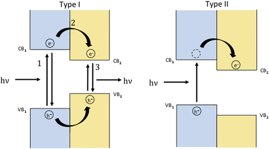
Figure 15. In type one alignment of the bands, photons can be absorbed if the energy of the incident light is above the respective band gaps, forming excitons. The kinetics of charge transfer between the constituents (labeled 2) and the ratio of initial absorption between the two constituents will determine the relative intensities of light emitted at the different band gap energies. In type II alignment, formation of the exciton occurs in one constituent layer and electrons will transfer into the adjacent material to achieve a lower energy state, resulting in an interlayer exciton. Since the constituents are separated only by the small van der Waals gap, the two charges remain bound.
Download figure:
Standard image High-resolution image
The discovery that monolayers of the group 6b dichalcogenides have direct band gaps and the discovery of fast charge transfer in heterostructures containing them has spawned research into the electronic properties of these systems and their derivatives. These dichalcogenides interact strongly with light at the ultimate monolayer limit [260] and host highly stable excitons (i.e. high binding energies, extended lifetimes) [56, 261, 262], which has resulted in exciting studies that either probe or exploit these properties. The substrate influences the excitons [154] but some properties, such as the conservation of spin-valley polarization during charge transfer between two monolayers, have been found to be only weakly dependent on the twist angle between layers [161]. The unique properties of dichalcogenide monolayers and the heterostructures built from them provides a promising platform for light–matter interaction experiments [260, 263] and has resulted in a continuing stream of papers building devices to take advantage of these properties. The devices include light emitting tunneling diodes [150], floating gate memory [156], photovoltaic devices [160, 264], and high sensitivity [151], broadband [153], and large area detectors [265]. Dichalcogenide nanosheets are also being explored as efficient photocatalysts and electrocatalysts for the production of hydrogen [187, 266, 267]. There has been considerable interest in the growth and properties of lateral heterostructures—in-plane junctions of two different dichalcogenides [250, 268]. Alloying either the transition metal [269] or the chalcogen [270] can be used to tune most of the important properties of these dichalcogenides, including structural phase transitions [271], band offsets [272], band gaps [273], and resulting device properties [68, 274]. This field is rapidly advancing, and ultimately the emergent properties of semiconducting TMD monolayers and heterostructures may find practical applications in lasers, light-emitting diodes, detectors, and photovoltaics. The next decade will see a significant growth in our understanding of the relationship between the structural nuances of TMD's in heterostructures, such as the importance of the interactions between layers, between constituents and substrates, between the active and protecting layers, and the resulting optoelectronic properties. This understanding will be of paramount importance for the efficient optimization of the emergent properties. The ability to construct novel heterostructures with reasonable assurance that they can be made provides value to predicting their properties. These predictions will significantly speed the development of this area.
4.2. Metallic heterostructures
The TMD, structurally related compounds, and other compounds that are potential heterostructure constituents offer a wide array of interesting properties that should, in principle, change as a function of thickness. While most of the early work has been on semiconducting monolayers, due to their novel emergent properties, the group IV and V group TMD offer additional and distinctly different opportunities. The group IV and group V TMD are semimetallic or metallic. There have been extensive studies aimed at understanding superconductivity, charge density waves (CDW), catalyst activity, and intercalation phenomena in the bulk group IV and V dichalcogenides [275–277]. The nanoscale thickness and monolayer properties of the metallic and semimetal compounds are less explored because they are typically less stable in normal atmospheric conditions than the semiconducting systems. For example, atomically thin NbSe2 [278] and TaS2 [279] have been reported to be unstable under ambient conditions. These stability challenges have been overcome by covering the sample with a protective layer [280] or by preparing a heterostructure containing the dichalcogenide layer of interest sandwiched between protective layers that are more stable under normal atmospheric conditions [281, 282]. Properties such as superconductivity and CDW have been shown to be thickness dependent, but as discussed below there are often considerable differences between literature reports.
There is an early body of literature that provides important structural data and ideas for the current interest in heterostructures containing isolated single nanosheets of layered group IV and V dichalcogenide compounds. Thermodynamically stable heterostructures of Ti, Cr and the group V dichalcogenides were prepared starting in the late 1980s by the groups of Wiegers [283], Meerschaut [284], Onoda [285] and Gotoh [286]. The properties of these compounds provide valuable insights for heterostructures being pursued today. These compounds were prepared by a direct reaction of the elements at high temperature, and are thermodynamically stable compounds. Single crystals can be grown using vapor transport reactions. As an example, combining Pb, Nb and Se and heating the elements to ∼1000 °C results in a so called misfit layered compound containing single NbSe2 layers separated by a unit cell thick layer of distorted PbSe [287]. The fact that this is stable relative to a mixture of PbSe and NbSe2 indicates that the interaction between the layers is strong, even though there is not an epitaxial relationship between the constituents. It has been suggested that charge transfer between constituents creates a significant electrostatic bond between the layers that stabilizes these compounds [288], although there is still considerable debate [289]. The physical properties change considerably as constituent layers are altered, and there are several extensive reviews reflecting significant interest in the structure and physical properties of these unusual compounds [15, 290]. None of these compounds have CDW transitions, but many of them are superconducting. Compounds with atoms containing magnetic moments, such as rare earth atoms, displayed magnetic order [15]. In these misfit layered compounds, the structure of each layer typically distorts to create one common in plane lattice parameter while the other axis is incommensurate (figure 3) [290].
Analogs of the crystalline misfit compounds can be prepared via low temperature synthesis routes. Compounds prepared by this route contain a random twist angle between layers, which, in the clay literature, is called turbostratic disorder [291]. These turbostratically disordered polymorphs, called ferecrystals, have been shown to have CDW, different superconducting properties than their analogous crystalline properties, and extraordinarily small thermal conductivities [292]. The variation of heterostructure properties as a function of constituent pairings and the rotation angle between them shows the importance of layer interaction in property determination. By extension, the surface on which a heterostructures is placed will also impact property measurements. The existence of thermodynamically stable misfit compounds—monolayers of dichalcogenides with a fragment of a 3D structure between them—suggests that there are many other heterostructures, combinations of 2D layers and 3D fragments of structures, that should be, at a minimum, kinetically stable.
The ability to predict the structures of layers and their potential combinations has already resulted in a significant theoretical effort exploring potential constituents, combinations of constituents, and their potential properties. The electronic structure and band alignment of monolayers of TMD in heterostructures has been systematically investigated, exploring interfacial charge polarization and redistribution [248]. Due to both the random twist angles between layers and the different lattice parameters for various constituents, the charge polarization and redistribution both deviate from conventional epitaxial semiconducting heterostructures based on tetrahedral semiconductors. Researchers have investigated structural and CDW phase transitions by probing how substrates, charge transfer between constituents, and electrostatic gating impact physical properties [293, 294]. Researchers have begun to explore the properties of 2D fragments of 3D structures, for example a unit cell (or two atomic planes) of the group IV monochalcogenides, in searching for potential emergent properties [295, 296]. The stability of CuS 2D layers as a function of thickness was recently reported [297]. The impact of the twist angle between ultrathin layers of Bi2Se3 [298] and the specific arrangement of different cations within a dichalcogenide layer [299] on potential topological states has been explored, as well. Extending these studies to probe potential heterostructures would be useful for experimentalists, and the misfit layer compounds provide an opportunity to compare predictions with experimental data. One aspect yet to be explored are the energy differences between different 2D slices of a 3D structure.
Experimentalists have also been exploring both new compounds and composites to probe for emergent properties. Research has explored doping known compounds with structures that appear to consist of interleaved 2d layers to create emergent properties that might be replicated in designed heterostructures. Knowing the distribution of the doping atoms between the layers is important for understanding the origin of superconductivity [222] and is important in determining the amount of modulation doping required to induce superconductivity in a heterostructure. Alemayheu et al showed that it is possible to prepare heterostructures containing fragments of 3D structures by preparing several new VSe2–GeSe2 heterostructures. In this report the thickness of the VSe2 block was varied while a monolayer of GeSe2 was maintained [197].
There has been considerable interest in finding a magnetic layer that could be used in the construction of heterostructures to probe topological properties and potential devices. One approach has been to create an interface between a magnetic insulator and a 2D layer to create a strong interfacial exchange field [158]. A second approach has been to find compounds containing magnetic ordering in layers that have strong bonding in a 2D layer separated by van der Waals bonding. The MPX3 family of compounds, where M is Mn, Cu, Fe, In, ... and X = S, Se, are semiconducting compounds due to strong electron correlation between the layers, but result in magnetic ordering within each layer of magnetic ions [226]. Ultrathin flakes of non-magnetic members of this same family have also been explored as ferroelectrics [300]. Heterostructures containing different thicknesses of SnSe and PbSe alternating with blocks of MSe2 trilayers (M = V, Nb, Ta) show systematic changes to the structure of the SnSe or PbSe block with thickness, and also display systematic changes in Hall coefficient and resistivity [112, 116, 282, 301, 302]. These results, while not inclusive of all that has been reported, illustrate the large number of potential heterostructures that can be prepared and several different approaches to discover emergent properties or optimize them for potential device applications.
A relatively general phenomenon that has been observed in both metallic monolayers and metallic heterostructures is an upturn in the resistivity as the temperature is lowered below approximately 30 K. This has been observed in NbS2 as the thickness is decreased [303] and also in a number of heterostructures [201, 281, 304]. In both the pure dichalcogenide and the heterostructures, the upturn becomes more pronounced as the thickness of the metallic layer is decreased. In the heterostructures, the upturn becomes more pronounced as increasing thickness of a semiconducting constituent separates the metallic dichalcogenide layer. The upturn in resistivity is not observed in crystalline metallic misfit layer compounds with identical composition and sequential layers as found in the ferecrystals, suggesting that the upturn is related to the disorder [305].
CDW transitions have been extensively explored in both heterostructures and as a function of thickness of dichalcogenide layers. This interest stems from the fundamental interest in the effect of dimensionality on the CDW [165, 306–310] and the potential use of CDW materials in optoelectronic devices [311] and quantum information processing [312]. Controlling the thickness of a dichalcogenide layer or the layer sequence and thickness in a heterostructures might potentially enable the CDW transition to be tuned to an optimal temperature or enable it to be controlled by an electric field [167, 313, 314]. A relatively large spread of reported CDW transition temperatures have been reported for nominally the same compound. For instance, an ordering temperature above 100 K was reported for atomically thin NbSe2 [165], while a lower ordering temperature CDW order (∼25 K) was reported for a monolayer NbSe2 grown on graphene [315]. There are several different reports on how the CDW changes as the number of VSe2 layers are reduced. VSe2 exhibits a CDW transition at 100 K in the bulk [316]. The onset of the CDW in thin layers of VSe2, prepared via liquid exfoliation, is 135 K as thickness is reduced to 4–8 trilayers [317]. Micromechanically exfoliated nanoflakes have lower onset temperatures which decrease to 81 K at the lowest thickness [307]. Studies of [(SnSe)1.15]m(VSe2)n prepared by annealing designed precursors have shown that compounds with a single layer of VSe2 separated by m layers of SnSe are p-type metals with a CDW that depends on the thickness of SnSe [302]. Increasing the VSe2 layer thickness to two or more layers results in low temperature n-type metals and the suppression of the pronounced effect in transport properties at the CDW transition temperature is similar to bulk VSe2 [318]. The influence of surface contaminations, the effect of different constituents, and/or the substrate on the CDW transition are only beginning to be explored or discussed in the literature. Encapsulation of the dichalcogenide layer of interest has been shown to enhance the CDW order in TiSe2 [319]. Similarly, TaS2 layers were encapsulated by covering them with boron nitride [279]. VSe2 layers prepared in situ from designed precursors have shown reproducible CDW transition temperatures and systematic changes as the thickness of either the VSe2 block or SnSe has been changed [302, 318]. These results suggest that much of the observed variability of results is a consequence of the instability of monolayers of the metallic dichalcogenides under ambient conditions. It might be possible to systematically control the CDW transition temperature of heterostructures through the choice of constituents and/or controlling the position of the Fermi level through modulation doping.
Given that some of the earliest investigations of ultrathin dichalcogenides by Frindt investigated superconductivity as a function of thickness, it is surprising that until recently there has been little attention directed in this area. This seems to have changed in 2016, with several high profile reports of well-defined 2D superconducting states in atomically thin NbSe2 [320], TaS2 [321] and doped MoS2 [322]. It is important to note that there were earlier reports of superconductivity in atomically thin flakes of NbSe2 prepared by mechanical exfoliation which demonstrated that the carrier density in these 2D layers could be changed by an electric field [323]. While traditionally carrier concentration is altered by chemical doping via atom substitutions, changing carrier density with an electric field minimizes potential complications such as impurity scattering. There have been several papers that show enhancement of the effective electron–phonon coupling constant, due to the change in phonon modes in monolayers [165, 278, 315]. All studies show a decreasing superconducting critical temperature as the thickness of the layers is decreased, although the values reported for samples of the same dichalcogenide with nominally the same thickness are different [131, 165, 278, 279, 305, 315, 320]. The variations may be due to different doping levels caused by neighboring layers or substrates, as Alemayheu reported a systematic increase in the Hall coefficient of (SnSe)1(NbSe2)n heterostructures as n was decreased to 1 [324]. A similar trend was observed in (PbSe)1(NbSe2)n layered structures [305], although the amount of charge transfer was different due to changes in the band alignment as SnSe [281] was replaced by PbSe [325]. Researchers exploring the superconducting and structural properties of FeSe layers on a variety of substrates have reported similar modulation doping effects [52, 132, 216, 326–333]. Adjacent layers or adsorbed surface species have begun to be used to investigate the interaction between two phenomena, for example superconductivity and ferromagnetism [334]. Monolayers are particularly sensitive to modulation doping, and phase transitions can be controlled by changing the Fermi level of adjacent layers through doping [51]. The investigation of superconductivity in 2D material is poised to see dramatic growth, as the ability to prepare stacks of constituents with different intrinsic properties will enable the interaction between phenomena to be investigated systematically.
The thermal conductivity of monolayer dichalcogenides and the heterostructures built from them has intrigued researchers since the first report, in 2007, of ultra-low thermal conductivity in heterostructures containing dichalcogenides [335]. Subsequent reports have reinforced the idea that the ultra-low thermal conductivity in the stacking direction of the turbostratically disordered heterostructures results from the random twist angles between adjacent dichalcogenide layers and between the various constituent layers [212, 336–338]. Low thermal conductivity of thermodynamically stable misfit layer compounds have been correlated with the density of stacking faults between adjacent layers [339]. The in-plane thermal conductivity of the heterostructures is a factor of 3–5 higher in the systems that have been measured, with the absolute value probably correlated with the in-plane grain size of the constituent layers [340]. The thermal conductivity of a monolayer has been calculated to also be anisotropic [341]. The ultra-low thermal conductivity of heterostructures provides opportunities to control the temporal features of heat pulses, which might be useful in designing phase change memory devices.
The very low thermal conductivity of heterostructures containing dichalcogenides has led to heterostructures being investigated as potential thermoelectric materials. Promising thermoelectric performance in dichalcogenide based materials have been reported for intercalates, due to the lowering of thermal conductivity and the ability to optimize carrier concentration [342, 343]. Low lattice thermal conductivity and promising un-optimized power factors have been reported for dichalcogenide monolayers [344, 345]. The thermodynamically stable misfit layered compounds have also been investigated as thermoelectric materials, with promising un-optimized figures of merit [346, 347]. The ability to prepare heterostructures of dichalcogenides with desired thicknesses of various constituents and targeted layer sequences provides an opportunity to optimize performance while gaining a better understanding of interactions and bonding between different constituent layers [348]. The ability to prepare heterostructures with junctions between constituents that have very different properties provides an avenue to increase efficiencies [349] and discover novel phenomena.
Topological phases, including topological insulators and Weyl semimetals have been the focus of recent attention, including the 2016 Nobel Prize in Physics to David Thouless, Duncan Haldane, and Michael Kosterlitz. Many of the most common materials studied for the topological properties consist of strongly bonded layers weakly connected by van der Waals bonding. For example, HfTe2, MoTe2 and WTe2 have all been reported to be topological Weyl semimetals [178, 350–353] while bismuth chalcogenides, Bi2Te3, Bi2Se3 and their alloys, are the prototypic topological insulators [354–367]. Both absolute size of the particles being investigated [368] and chemical doping have been used to produce new phenomena [369]. From a materials perspective, heterostructures containing very thin constituent layers might be useful in reducing contributions from the bulk, enabling exotic topological states to be both easier to study and utilize. Heterostructures also potentially provide an avenue to prepare materials with different properties adjacent to one another [370], for example a ferromagnetic layer adjacent to a superconducting layer, with a defined interface between them. The use of heterostructures to probe topological properties is just beginning.
5. Summary
The ability to prepare and manipulate monolayers of dichalcogenides and other 2D materials as building blocks for heterostructures provides scientific challenges and opens new opportunities. Challenges include:
- Developing approaches to synthesize heterostructures over large areas with control of individual constituent layer thicknesses and the sequence of layers.
- Advancing measurement techniques to characterize the local composition and structure of each constituent layer.
- Developing theoretical approaches to predict band alignments, the extent of charge transfer between constituents, structural distortions and properties of heterostructures with incommensurate interfaces.
The new opportunities include:
- Predicting the structure of an essentially infinite number of new heterostructures, enabling theorists to predict the properties of compounds yet to be made.
- Creating interfaces where atoms are in unusual coordination environments, potentially leading to the discovery of more emergent properties.
- Designing heterostructures that combine multiple technologically desirable functionalities in adjacent constituent layers that tend not to co-exist.
- Using the concept of an energy landscape to develop synthetic routes to the infinite number of potential metastable heterostructures.
Tremendous progress has been made in the past decade developing approaches to make monolayers of specific compounds, understanding the origin of emergent properties at the monolayer limit, and identifying how properties change as monolayers are placed on different substrates. Understanding how incommensurate layers interact, how different combinations of constituents lead to emergent properties, and how to utilize new properties in devices are likely to dominate this field of research in the coming decade. The potential outcome of these efforts will be materials by design, with constituents and nanoarchitecture of heterostructures optimized for predicted emergent properties and the desired function of the total material in a specific device.
Acknowledgments
The authors acknowledge support from the National Science Foundation under grant DMR-1266217.