
Abstract
We demonstrate high-performance normally-off multi-fin β-Ga2O3 vertical transistors with a wide fin width from 1.0 to 2.0 μm by using a nitrogen-doped β-Ga2O3 high-resistive layer grown by halide vapor phase epitaxy. Normally-off operation was achieved with a threshold voltage of ≥1.3 V, a specific on-resistance of 2.9 mΩ·cm2 and a current density of 760 A cm−2 at a gate voltage of +10 V. The estimated MOS channel field effect mobility was ∼100 cm2 V−1 s−1. These findings offer important insights on the development of Ga2O3 MOSFETs and show the great promise of Ga2O3 vertical power devices.
Export citation and abstract BibTeX RIS
Beta gallium oxide (β-Ga2O3) has become of interest in the power electronics industry especially for electric vehicles, power conditioning, power distribution, and switching applications, owing to its large bandgap (4.5–4.9 eV), high theoretical breakdown electric field (6–8 MV cm−1), and Baliga's figure of merit (FOM) exceeding that of Si, SiC and GaN. To date, fabrication of devices using β-Ga2O3 has been actively carried out. 1–9) Lateral transistors with a breakdown voltage of up to 8 kV 10) and vertical transistors with a breakdown voltage of 2.6 kV 11) and 5 kV 12) have been also demonstrated. So far, normally-off characteristics have been realized with a recessed gate structure in lateral transistors and a submicron fin-channel structure in vertical transistors without p-type doping 11–13) because of the difficulty in fabricating a p-type conductive layer of β-Ga2O3. However, the threshold voltage (Vth) of these devices strongly depends on the recess depth or the submicron fin width. Therefore, it is difficult to fabricate mm-size power devices on conventional 4 and 6 inch mass-production lines. β-Ga2O3 high-resistive p-like-well structures whose Vth depends on the dopant concentration of deep acceptors such as nitrogen (N) 14–16) and magnesium (Mg) 16–18) have been investigated as alternative structures in which Vth does not strongly depend on the recess depth or fin width. In particular, a lateral transistor using a thin N-doped layer grown by molecular beam epitaxy 19) and a vertical U-shaped trench gate metal-oxide-semiconductor field-effect transistor (MOS FET) using an N-ion implantation layer 20) were reported to have normally-off characteristics. However, the former transistor operated only in the subthreshold region and the later transistor required a large positive gate-bias voltage (Vgs) of 25 V for operation due to a nonoptimized dose of N+ implantation. In this paper, we report high-performance normally-off multi-fin β-Ga2O3 vertical transistors (Vth ≥ 1.3 V, Ron,sp = 2.6 mΩ·cm2 @Vgs = 10 V, μFE ∼ 100 cm2 V−1 s−1) in which the fin width has little impact on Vth; they have a thick N-doped β-Ga2O3 high-resistive layer grown by halide vapor phase epitaxy (HVPE).
The schematic device structure is shown in Fig. 1(a). To evaluate the MOS channel mobility, a 3.3 μm N-doped Ga2O3 well layer was grown by HVPE on a (001) n+-β-Ga2O3 substrate without a drift layer. The first n+ layer ([Si]≈ 1 × 10¹⁶–8 × 1018 cm−3, 650 nm depth) was formed on the surface by Si implantation 21) up to 500 nm depth and diffusion up to 650 nm depth by annealing the Si at 1000 °C for 30 min under N2 to connect the MOS channel to the source contact region. The second n+ layer ([Si] ≈ 6 × 1019 cm−3, 200 nm depth) was formed on the top surface to facilitate the source ohmic contact by Si implantation and annealing at 900 °C for 1 min under N2. Doping profiles under the source after device fabrication were confirmed by secondary ion mass spectrometry (SIMS; Fig. 2). The thickness of the non-Si-implanted and diffused layer was 2.6 μm, where the N concentration was ∼1.0 × 1016 cm−3, Si concentration was ∼3.0 × 1015 cm−3 or less, and Cl concentration was ∼2.0 × 1015 cm−3. The source of N was most likely the N2 carrier gas during HVPE growth. After Si implantation and diffusion, the SiO2 etch mask was deposited by plasma-enhanced chemical vapor deposition (PECVD). Fin channels were defined by electron beam lithography and formed by dry etching using CHF3 and BCl3. The resultant fin channels had a near-vertical sidewall profile [Fig. 1(b)]. After dry etching, the wafer was treated with HF for 15 min to remove the SiO2 etch mask and plasma-damaged layer. Then, 53 nm SiO2 gate dielectric was deposited by atomic layer deposition and was post-deposition annealing at 800 °C for 10 min. 70 nm Cr gate metal was deposited by electron beam evaporation (EBE). Next, a thick SiO2 spacer was deposited by PECVD from the bottom to the top of the fins. The SiO2 spacer and Cr gate metal were etched to 600 nm below the fin top by dry etching using CHF3 and Cl2/O2. Then, a thick SiO2 spacer was deposited by PECVD again on the top of the fin. After removing the SiO2 on the fin top, the source electrode (Ti/Au) on the fin top and the drain electrode (Ti/Au) on the back side of the n+-β-Ga2O3 substrate were deposited by EBE.

Fig. 1. (Color online) (a) Schematic cross-section of Ga2O3 vertical fin transistors with multiple fins. (b) Scanning electron microscopy (SEM) cross-section image of a fin channel. (c) Optical image of a multi-fin device with a fin width of ∼2.0 μm and fins rotated clockwise by 60°.
Download figure:
Standard image High-resolution image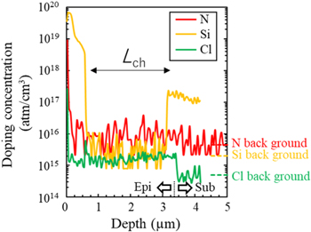
Fig. 2. (Color online) SIMS of 0.65 μm depth Si-implanted 3.3 μm thick N-doped Ga2O3 epitaxial layer on Sn-doped Ga2O3 substrate.
Download figure:
Standard image High-resolution imageFigure 1(c) shows top views of the fabricated multi-fin devices. Defining 0° as a fin with (100)-like sidewalls along the [010] direction, the devices with fins rotated clockwise by 60° were evaluated. The fin widths (Wfin) of the devices were 1.0, 1.5, and 2.0 μm, and the pitches were 6.0, 6.5, and 7.0 μm, respectively. The devices comprised 14 fins side by side, and 10 of them were covered with the source electrode. This is because the fins on the outside of the pattern tended to have large errors from the designed dimensions during the dry etching process.
The dependence of the transistor transfer characteristics and Vth on the Wfin is shown in Figs. 3(a), 3(b). Here, current density (J) is normalized by the active area A (fin number of 10 × pitch × fin length of 60 μm). Vth is linearly extrapolated from the Jd–Vgs characteristic between Vgs = 2 and 3 V. The device characteristics discussed are those after Vth stabilization, unless otherwise specified. From Fig. 3(a), these devices showed Vth exceeding 1 V regardless of the Wfin, an on–off ratio >108, and current densities >1 A cm−2 (Vgs = 3 V, Vds = 0.1 V). In this experiment, Jd max decreased as the Wfin decreased. This is because of the etch-back process of SiO2 optimizing for Wfin = 2 μm pattern, so the top of the gate electrode was lowered from the Si-doped n+ layer when Wfin was decreased to 1.5, 1.0 μm, and the source-channel resistance drastically increased. Figure 3(b) shows the Wfin dependency of Vth. The open and closed circles indicate the experimental results of Vth and the solid and dotted lines indicate the calculation of Vth for n-channel FinFETs. The open and closed circles indicate the fresh and stabilized Vth, extracted from the first upward transfer Jd–Vgs sweep and the subsequent Jd–Vgs sweep. In the subsequent Jd–Vgs sweep, Vth increased by 0.3–0.6 V and stabilized. This instability is attributed to the increase in the negative interface charge density due to the electron trapped at the MOS interface or inside SiO2. The trapped electron density was estimated to 1.2–2.6 × 1011 cm2. Because these traps have a long emission time constant, it takes more than two weeks to return to the fresh state from the stabilized state. The lines show the dependence of the calculated Vth on Wfin for n-channel FinFETs. The Vth was obtained by the following formula (1):

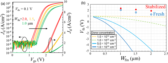
Fig. 3. (Color online) (a) Transfer Jd–Vgs characteristics of the vertical transistors with different channel widths. (b) Dependence of Vth on the fin channel width. The closed circles indicate the experimental result obtained in this experiment. The solid lines indicate the calculated Vth for n-channel FinFETs.
Download figure:
Standard image High-resolution imageVth: threshold voltage, φms: work function difference between metal and semiconductor.
ND: donor concentration, W: Wfin/2, ε0: vacuum permittivity.
εs: relative permittivity of Ga2O3, Cox: capacitance of oxide film.
As shown by the solid lines, at the ND of 0.5–1.0 × 1016 cm−3, that is, the lowest value demonstrated by HVPE, Vth depends greatly on the Wfin, and a Wfin of 0.4–0.5 μm or less is required to obtain normally-off characteristics. On the other hand, as shown by the dashed lines, if the ND could be reduced to 1.0 × 1014 cm−3, Vth became less dependent on the Wfin and normally-off characteristics can be obtained even at 1 μm or more. In the N-doped channel, the concentration of deep acceptor impurity (N) is higher than that of donor impurity (Cl and Si) as shown in Fig. 2. Therefore, donors are fully compensated by deep acceptors in N-doped channel and Vth becomes less dependent on the Wfin. Furthermore, the deep acceptor level may raise the Fermi level in N-doped channel to further increase Vth.
Figure 4(a) shows the Jd–Vgs characteristics of a device with a Wfin of ∼2.0 μm. The device has a Vth of ∼1.9 V (Vds = 0.1 V) and an on–off ratio of >108. The subthreshold slope is ∼90 mV dec−1. Figure 4(b) shows the estimated field-effect-mobility of the N-doped MOS FET. The field-effect-mobility of ∼100 cm2 V−1 s−1 is two-third of a hall-mobility (150 cm2 V−1 s−1) of an unintentionally doped epitaxy layer (ND-NA = 1 × 1016 cm−3) by HVPE. The FET was estimated using the formula (2):

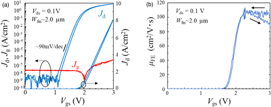
Fig. 4. (Color online) (a) Transfer Jd–Vgs characteristics with a Wfin of ∼2.0 μm and pitch size of 7.0 μm. (b) Field effect mobility characteristics with a Wfin of ∼2.0 μm.
Download figure:
Standard image High-resolution imageThe one channel current is 1/20 of the drain current ID (the device has 10 fins which have two sidewalls in the active area A), the channel length Lch (2.6 μm) obtained from SIMS profiles in Fig. 2, the channel width equal to the fin length Lfin (60 μm), dielectric constant εr (4.06) of the gate insulating film estimated from the MOS capacitor on the same wafer, and SiO2 thickness tOX (53 nm). High electron mobility of 100 cm2 V−1 s−1 will be obtained by reducing the roughness scattering and coulomb scattering at the MOS interface, because the low N acceptor concentration (1.0 × 1016 cm−3) in the channel reduces the effective electric field at the MOS interface under positive gate-bias condition. This mobility is attractive for 600–3000 V MOS FET applications, where Ron,sp has been limited by the MOS channel resistance being proportional to inverse of the channel mobility.
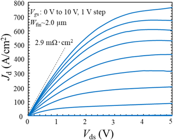
Figure 5 shows the Jd–Vds characteristics of a device with a Wfin of ∼2.0 μm. Ron,sp was determined to be 2.9 mΩ·cm2 (Vgs = 10 V) and Jd = 760 A cm−2 (Vgs = 10 V, Vds = 5 V). The calculated Ron,sp contains the substrate series resistance, 1.5 mΩ·cm2 (ND = 4 × 1018 cm−3, μ = 47 cm2 V−1 s−1, t = 550 μm); therefore, the actual MOS channel resistance Rch,sp should be 1.4 mΩ·cm2.
Fig. 5. (Color online) Output Jd–Vds characteristics.
Download figure:
Standard image High-resolution image
In conclusion, high-performance normally-off β-Ga2O3 vertical FETs were demonstrated. The fin width's impact on Vth was reduced by introducing an N-doped β-Ga2O3 high-resistive layer grown by HVPE. An Ron,sp of 2.9 mΩ·cm2, Jd of 760 A cm−2, and mobility of ∼100 cm2 V−1 s−1 were achieved in multi-fin devices. These results are a significant step forward in the development of β-Ga2O3 power transistors.
Acknowledgments
This work was supported by Innovative Science and Technology Initiative for Security Grant Number JPJ004596, ATLA, Japan. A part of this work was conducted at NIMS Nanofabrication Platform, supported by "Nanotechnology Platform Program" of the Ministry of Education, Culture, Sports, Science and Technology (MEXT), Japan, Grant Number JPMXP09F21NM0009.