

Abstract
Gallium nitride (GaN) is becoming a mainstream semiconductor for power and radio-frequency (RF) applications. While commercial GaN devices are increasingly being adopted in data centers, electric vehicles, consumer electronics, telecom and defense applications, their performance is still far from the intrinsic GaN limit. In the last few years, the fin field-effect transistor (FinFET) and trigate architectures have been leveraged to develop a new generation of GaN power and RF devices, which have continuously advanced the state-of-the-art in the area of microwave and power electronics. Very different from Si digital FinFET devices, GaN FinFETs have allowed for numerous structural innovations based on engineering the two-dimensional-electron gas or p–n junctions, in both lateral and vertical architectures. The superior gate controllability in these fin-based GaN devices has not only allowed higher current on/off ratio, steeper threshold swing, and suppression of short-channel effects, but also enhancement-mode operation, on-resistance reduction, current collapse alleviation, linearity improvement, higher operating frequency, and enhanced thermal management. Several GaN FinFET and trigate device technologies are close to commercialization. This review paper presents a global overview of the reported GaN FinFET and trigate device technologies for RF and power applications, as well as provides in-depth analyses correlating device design parameters to device performance space. The paper concludes with a summary of current challenges and exciting research opportunities in this very dynamic research field.
Export citation and abstract BibTeX RIS
1. Introduction
Relentless scaling of silicon (Si) complementary metal–oxide–semiconductor (CMOS) transistors over the past several decades has allowed integrated circuits (ICs) with extraordinary performance. The fin field-effect transistor (FinFET) has been the key device to enable scaling for technology nodes below 22 nm [1]. This device employs multiple-gate architectures and nanometer-sized fin-shaped channels [2–8]. Compared to conventional planar metal–oxide–semiconductor field-effect transistors (MOSFETs), the presence of multiple gates around each fin in a FinFET allows for superior gate control of channel electrostatics and therefore significantly alleviates short-channel effects, the major roadblock for transistor scaling. Depending on the number of sides of the fin channel that are covered by the gate metal, FinFETs are referred to as dual-gate, trigate, or gate-all-around transistors [9]. Since the first half of the 2010s, Si FinFETs have become the backbone technology for high-performance digital and memory applications. The global FinFET market reaches over $42 billion in 2019 [10].
Beyond Si, gallium nitride (GaN) has recently become a mainstream material for power electronics and radio-frequency (RF) applications. As shown in table 1, compared to Si, GaN has superior physical properties for high-voltage, high-frequency and high-power applications, including the large bandgap, high critical electric field, and high saturation velocity. In addition, the AlGaN/GaN hetero-structure allows for the formation of a two-dimensional electron gas (2DEG) and fabrication of high-electron-mobility transistors (HEMTs) [11]. After two decades of relentless development, GaN RF HEMTs have been commercialized for telecom and defense applications [12], with market size of $740 million in 2019 [13]. In the meantime, GaN power HEMTs have been recently commercialized for 15–650 V power switching applications. They are now seeing rapid adoption in power supplies, data centers, Lidar systems, and the fast charging systems in consumer electronics [14–16].
Table 1. Material properties of major commercially available semiconductors for power and RF applications.
| Si | GaAs | SiC | GaN | |
|---|---|---|---|---|
| Eg (eV) | 1.1 | 1.4 | 3.3 | 3.4 |
| µe (cm2V−1 s−1) | 1400 | 8000 | 1000 | 2000 (2DEG) |
| Ec (MV cm−1) | 0.3 | 0.4 | 2.5 | 3.3 |
| kT (W cm−1 K−1) | 1.3 | 0.46 | 4.2 | 1.3–2 |

| 11.8 | 12.9 | 9.7 | 9 |
| vsat (×104 m s−1) | 1 | 1.5 | 2.0 | 2.5 |
Baliga's FOM ( ) ) | 1 | 15 | 340 | 1450 |
| Johnson's FOM (vsat Ec) | 1 | 2 | 17 | 27.5 |
Eg: bandgap; µe: electron mobility; Ec: critical electric field; kT: thermal conductivity;  : dielectric constant; vsat: saturation velocity.
Despite the initial success, the performance of commercial GaN RF and power devices has not yet reached the GaN material limit. In the last few years, GaN FinFETs and trigate devices have arguably been among the most innovative, fast-developing, and promising GaN devices for both power and RF applications. These nonplanar GaN devices take advantage of the multi-gate fin channels to improve the gate controllability and suppress the short-channel effects, which have not only enabled higher current on/off ratio and steeper subthreshold swing (SS) similar to the Si counterparts, but also brought many merits particularly desired for power and RF applications. In this work, the GaN FinFET mainly refers to the GaN devices with two sides of the fin channel covered by the gate metal, while the GaN trigate devices have three sides of the fin channel covered by the gate metal.
Conventional planar GaN HEMTs are depletion-mode (D-mode). However, enhancement-mode (E-mode) transistors are highly preferable for power electronics applications to allow safe operation and circuit simplification. GaN fin-based HEMTs can realize E-mode operation by combining two effects: (a) enhanced 2DEG depletion due to the depletion by sidewall gate stacks, and (b) the reduced piezoelectric polarization and 2DEG density due to partial strain relaxation in the AlGaN barrier of narrow fins [17]. Compared to other E-mode structures such as gate recess and p-GaN gate, the FinFET or trigate devices retain the 2DEG channel in the gate region and allow tight gate control of the 2DEG channel, therefore realizing excellent gate controllability and a low channel resistance in the gate region simultaneously. In addition, the superior gate control reduces the drain-to-source leakage current at high blocking voltages, leading to superior device reliability and lower off-state power loss. Finally, the trigate structure can alleviate the electric field (E-field) crowding at the drain-side gate edge, therefore suppressing the dynamic on-resistance (Ron) and current collapse [18, 19].
A benefit of using the FinFET and trigate structures in RF GaN HEMTs is the suppression of short-channel effects, which allows aggressive gate length scaling and potentially a high unity current-gain frequency (fT) [20]. The high fT, in conjunction with the reduced output resistance in highly-scaled devices, potentially enables a high unity power-gain frequency (fmax) [21], if the fin-induced parasitic capacitance is appropriately managed. In addition, trigate GaN HEMTs can realize a significantly improved linearity through fin geometry engineering [22–25] and reach the peak transconductance (gm) for smaller gate voltage swings [23], which are both highly desirable in circuit applications. Finally, the current distribution in large area nonplanar fin structures favors heat dissipation and can improve the thermal performance of power and RF GaN HEMTs [26, 27].
While lateral HEMTs are advantageous for high-frequency and low-voltage applications, the vertical device is favored for high-voltage, high-power applications [28]. The vertical structure eases current spreading and thermal management [29] and can realize high voltage and high power without enlarging the chip size [30, 31]. It is used in commercial medium-voltage (650 V–1700 V) and high-voltage (>1700 V) power devices and high-power RF devices in Si and SiC.
Recently, the FinFET structure has also been leveraged to develop medium-voltage vertical GaN power transistors on Si, engineered substrate, and free-standing GaN substrate [32–35]. The fin channel enables the E-mode operation by fin width scaling and features bidirectional unipolar conduction that has no reverse recovery. In addition, the small footprint of fin channels allows much higher channel density when compared to conventional power MOSFETs. 1200 V vertical GaN-on-GaN power FinFETs have shown one of the highest static figure-of-merits (FOMs) [33, 36, 37] and switching FOMs [34] in all medium-voltage GaN, Si, and SiC power transistors. The avalanche capability, which is highly desirable in many power applications such as motor drives and grid inverters but lacking in GaN HEMTs [38–40], has also been demonstrated in 1.2 kV vertical GaN FinFETs [36, 37], which represent the first avalanche GaN power transistors.
Very recently, lateral trigate GaN HEMT and vertical GaN FinFET device technologies have been successful transferred from the lab to large volume fabs, and are in the process of being commercialized by several companies. In spite of the fast advancements in GaN FinFET research, papers that provide a global overview of GaN FinFETs for RF and power applications are scarce. We recently provided a tutorial and survey on vertical power FinFETs based on GaN and other ultra-wide-bandgap semiconductors [41], but that paper focuses on vertical devices. In this article, we aim at reviewing the lateral and vertical GaN FinFETs and trigate devices published so far for both power and RF applications, in order to provide an overview and comprehensive perspective that serves as a roadmap for future device development.
This article is organized as follows: section 2 describes the device structures and major variations of GaN FinFETs and fin-based HEMTs; sections 3 and 4 provide an overview of GaN FinFET/trigate devices for power and RF applications, respectively; section 5 presents an in-depth analysis and modeling that correlates the key device parameters to the device performance metrics; section 6 provides a perspective of current challenges and research opportunities on GaN FinFETs and trigate devices; section 7 summarizes the key conclusions of the paper.
2. Device concepts and structures
2.1. Lateral FinFET and trigate HEMT
Figures 1(a) and (b) show two basic architectures of the lateral GaN FinFETs, the first type with the fin-shaped channels extending across the entire source-to-drain region and the second type with the fin-shaped channel only present in the gate region. The first type of GaN FinFETs is similar to the digital FinFET, and it can be fabricated either through the bottom-up growth of GaN nanowire (NW) transistors [42–44] or through top-down etching of a planar GaN structure [45–48]. This latter device is often called 'nanoribbon (NR) GaN HEMT.'

Figure 1. 3D schematic of lateral GaN FinFETs and trigate HEMTs with (a) fins extending between source and drain and (b) fins only in the gate region. (c) Cross-sectional schematic of three types of fin bodies and (d) the current conduction paths (illustrated in yellow) in each type of fin body. (e) Cross-sectional schematic of three types of gate stack in the trigate.
Download figure:
Standard image High-resolution imageWhile the NR GaN HEMTs allow strong carrier confinement, the 2DEG density in the NR was found to be very sensitive to mechanical stress, which can be easily influenced by passivation dielectrics and dielectric thickness [47, 49, 50]. In addition, the fin-shaped channels in the access regions induce higher access resistance and limit the current density normalized with the entire device area. As a result, the second type of FinFET (figure 1(b)), often referred to as the trigate HEMT, later became a more popular device of choice for GaN RF and power FinFETs.
A unique feature of the GaN FinFET that differs from the Si FinFET is the diversity in fin bodies. While Si fins usually employ an intrinsic or doped body, GaN FinFET bodies can be made of doped GaN, AlGaN/GaN heterojunction, and multiple heterojunctions (see figure 1(c)). In power and RF applications, devices are used as solid-state switches and amplifiers, and they usually operate in the linear or saturation regime, respectively, instead of the sub-threshold regime. The different device operation regimes suggest different current paths in GaN fins compared to the ones in digital Si FinFETs. As shown in figure 1(d), after the device turn-on, current can flow simultaneously through the bulk fin and the two sidewall accumulation-mode metal–oxide–semiconductor (MOS) channels in the heterojunction-free fins, and through the 2DEG channel and sidewall MOS channels in the heterojunction fins. In heterojunction fins, the 2DEG can be modulated by the fringing E-field from the top gate and two sidewall gates; in multi-channel fins, the buried 2DEG channels are mainly controlled by the sidewall gates.
Figure 1(e) illustrates three main types of gate stack in GaN trigate devices. The first trigate HEMTs were demonstrated based on Schottky-type gates by Tamura et al [51] and Ohi and Hashizume [52]. These Schottky-type trigate HEMTs were initially named as the multi-mesa-channel (MMC) HEMTs [51–54] or the nanochannel array HEMTs [55], depending on the degree of fin width scaling. More recently, trigate GaN HEMTs have adopted the MOS and the metal–insulator–semiconductor (MIS) gate stacks, which have gradually become the prevailing choice of gate stack in GaN trigate HEMTs. Compared to the Schottky-type trigate, the MIS/MOS-type trigate significantly reduces the gate leakage current and increases the gate voltage (VG) operation range.
Recently, Ma and Xiao et al proposed a new trigate configuration, the junction trigate, in which the p–n junction wraps around the heterojunction fins and the gate metal forms Ohmic contact to the p-type material [56]. Owing to the higher built-in potential and the obviation of voltage drop in the insulator, the p–n junction can potentially provide a stronger depletion compared to the MIS/MOS stack, making it easier to realize E-mode operation and suppress short-channel effects. In addition, the junction trigate can eliminate the sidewall MOS channels and therefore avoid the potential gate dielectrics reliability issues.
2.2. Vertical FinFET
Vertical power/RF FinFET combines the sub-micron fin-shaped channels to provide superior gate control and a lightly-doped, thick drift region to accommodate the large current, high voltage, and high power. The concept of using multiple gates to control a vertical channel on top of a drift region dates back to static induction transistors (SITs) and power junction field-effect transistors (JFETs). The SIT, first proposed in the 1950s and realized in the 1970s [57], possesses Schottky- or p–n-type gate stacks residing in recessed trenches [58]. The SIT is typically D-mode and pinched off by channel depletion at negative VG. Commercial SiC SITs are now available for high-frequency power amplification applications with voltage up to 125 V [59, 60]. The SiC JFET has a similar structure but is developed for high-voltage power applications. While the vertical channel is n-type, the gate typically locates at the trench bottoms that are implanted to become p+-type. Both normally-off [61] and normally-on [62] SiC JFETs have been recently commercialized from 650 V to 1.7 kV [63].
Figure 2(a) shows the schematic of a vertical Fin-MOSFET. A key feature that differentiates the vertical Fin-MOSFET with SITs and JFETs is the sidewall MOS stack that allows parallel current conduction through the bulk fin and the two accumulation-mode MOS channels [64]. This sidewall MOS channel can significantly reduce the channel on-resistance and increase the current density. In addition, the vertical Fin-MOSFET only needs n-type layers and does not require epitaxial regrowth, making it attractive for many emerging semiconductors where only one type of doping is viable [41]. A recent review of wide-bandgap and ultra-wide-bandgap vertical power Fin-MOSFETs is presented in [41].
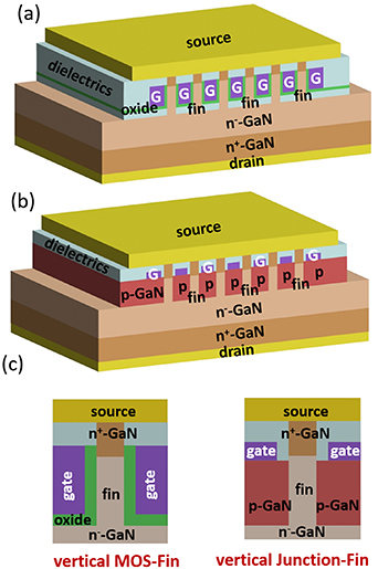
Figure 2. 3D schematic of (a) vertical GaN Fin-MOSFET and (b) vertical GaN Fin-JFET. (c) Cross-sectional schematic of a unit-cell of vertical GaN Fin-MOSFET and Fin-JFET.
Download figure:
Standard image High-resolution imageFigure 2(b) shows the schematic of a vertical GaN Fin-JFET, which has a similar structure with SiC JFET but typically has an increasingly scaled fin width with the p-GaN fully filling the inter-fin trenches. The fabrication of vertical GaN Fin-JFET usually relies on the selective-area p-GaN epitaxy [65, 66], which can potentially allow better control of dopant diffusion when compared to the ion implantation used in SiC JFET fabrication. The fin-JFET retains the merits of the fin channel, making it easier to realize the avalanche breakdown [36, 37], and can potentially eliminate the oxide reliability issues that have been revealed to be a critical concern in SiC MOSFET [67] particularly at high temperatures [68, 69].
Vertical power FinFETs can be built on either a fully vertical structure (figure 2) or a quasi-vertical structure where the drain locates at the bottom of a deeply recessed mesa on the same side of the wafer as the source and gate [35, 70–73]. The fully vertical structure usually employs a free-standing n+-GaN substrate. In contrast, the quasi-vertical structure allows the fabrication of vertical GaN devices on foreign substrates, e.g. Si substrate (which is widely used in lateral GaN HEMTs). The GaN epitaxy on GaN substrates typically provides lower dislocation density compared to the one on foreign substrates, which enables lower leakage current in vertical devices [74]. Whereas, the GaN-on-Si and GaN-on-sapphire wafers provide cost advantages. Alternatively, GaN grown on engineered substrates (QST®) with a matched thermal expansion coefficient could enable low-cost vertical GaN FinFETs with thick (>10 μm) drift layers and large wafer diameters (8–12 inch) [35]. It should be noted that fully-vertical devices can also be fabricated in GaN-on-Si by a variety of approaches, including the layer transfer [73, 75], buffer doping [76, 77], and deep backside trenches [78, 79]. The performance and cost trade-offs between the full-vertical and quasi-vertical GaN devices have been thoroughly reviewed and discussed in [31], which will not be the focus of this paper.
3. GaN FinFETs and trigate devices for power applications
3.1. Lateral power FinFETs and trigate HEMTs
The first trigate HEMT with over 100 V blocking voltage was demonstrated by Ohi and Hashizume in 2009 [52], based on the Schottky-type trigate (i.e. MMC HEMT). A fin width (WFin) down to 70–90 nm allows a positive shift in threshold voltage (VTH) to −2.5 V. A breakdown voltage (BV) of 250 V was reported. The device Ron is found to be dominated by the channel resistance in the gate region [54], making the drain current (ID) insensitive to access resistance. Reduced current collapse [53] and thermal resistance [26] were also reported in this D-mode Schottky-type trigate HEMT.
The first E-mode medium-voltage trigate HEMT was reported by Lu et al in 2012 [80] using an MIS-type trigate. To increase VTH, an additional AlGaN barrier recess was implemented in part of the top region of the 120 nm wide fins (figure 3), allowing a VTH over 0.8 V from linear extrapolation in the transfer characteristics. The device shows a BV of 565 V extracted at ID of 0.6 µA mm−1 and VG of 0 V.

Figure 3. 3D schematic of the trigate HEMT with an additional AlGaN barrier recess in the fin-gate region.
Download figure:
Standard image High-resolution imageHeterostructure-free power GaN FinFETs were reported by Im et al in 2013 [81, 82], with a WFin down to 60 nm, a VTH up to −1.5 V, and a destructive BV of 600 V. The comparison between GaN FinFETs and AlGaN/GaN FinFETs reveals that [82, 83], though the AlGaN/GaN FinFET has higher channel mobility, it exhibits a more pronounced WFin dependence of Ron and an increased susceptibility to short-channel effects due to the high electron concentration in 2DEG.
Since 2017, Ma et al [84–87] have reported continued performance advancements in D-mode trigate power HEMTs by optimizing the fin geometry to enhance BV and using stacked 2DEG channels to lower Ron. With a higher filling factor [i.e. WFin/(WFin + SFin), where SFin is the fin spacing], a 792 V BV and 0.91 mΩ cm2 Ron were reported in D-mode trigate HEMTs [84]. A slanted trigate structure was proposed in [85], where the fin width increases from 350 nm at the source side of the gate to 700 nm at the drain side of the gate. This slanted trigate allows reducing the E-field crowding at the gate region and enables a BV to increase up to 1350 V at ID of 1 µA mm−1 [85]. In 2018, Ma et al reported a five-2DEG-channel trigate HEMT, which demonstrates a 47% smaller Ron compared to the single-channel trigate HEMT [87]. In 2019, Ma et al reported a superior BV and Ron trade-off (1230 V/0.47 mΩ cm2, where BV is extracted at ID of 1 mA mm−1) in a D-mode GaN power HEMT that combines the multi-channel structure and the slanted trigate structure [86] (figure 4).

Figure 4. Schematic of the multi-channel trigate HEMT with slanted-shape trigate reported in [86]. Reprinted with permission from [86], © (2019) IEEE.
Download figure:
Standard image High-resolution imageSince 2019, multiple groups have reported performance advancements in E-mode trigate power HEMTs. Nela et al demonstrated an E-mode fin-based MOS gate with a planar gate using high work-function (WF) metals [88]. Without metal coverage into the inter-fin trenches, this structure allows the scaling of WFin and SFin both down to below 40 nm, with the high-voltage E-mode operation being realized when WFin is reduced to 20 nm. Zhu et al [89] and Huang et al [90] reported MIS-type trigate HEMTs with additional gate recess, similar to Lu's work in 2012, but with enhanced performance by either integrating a gate field plate [89] or replacing the AlGaN/GaN barrier with an InAlN/GaN barrier [90], respectively. The InAlN/GaN barrier has a higher 2DEG density and stronger spontaneous polarization; hence, the partial strain relaxation and VTH shift are more pronounced in narrow fins. Recently, Huang et al reported further reductions of the off-state leakage current in trigate InAlN/GaN power MIS-HEMTs by using a Schottky tri-drain extension [91].
An E-mode trigate MIS-HEMT using a novel ferroelectric charge-trapping dielectrics was reported by Wu et al [92]. The trapped negative charges in the periodic HfZrO4/Al2O3 gate dielectrics lift VTH, which obviates the additional gate recess and relaxes the need for aggressive WFin scaling to realize the positive VTH. This further reduces Ron in the gate region and improves the current density [92]. However, it should be noted that the charge-trapping dielectrics necessitate a high gate bias (12 V) stress for the initialization process that fills the traps and converts the trigate device from the D-mode into the E-mode operation. The thermal stability of this trapped dielectrics and the relevant de-trapping time have not been reported, which may be a concern for the long-term and high-temperature operation of power devices.
While all the prior D-mode and E-mode trigate HEMTs rely on the Schottky gate or the MIS gate, Ma and Xiao et al recently demonstrated a trigate GaN junction HEMT using the heterogeneous p–n junction between p-NiO and 2DEG [56]. As shown in figure 5, the gate metal Ni forms Ohmic contact to p-NiO, and the hole concentration in NiO is above 1019 cm−3, allowing the entire WF difference between Ni and GaN to fall on GaN for fin depletion. Owing to the stronger depletion in the junction trigate when compared to the MIS trigate, a higher VTH was reported in trigate junction HEMTs than that in the trigate MIS-HEMTs with the same WFin. This stronger depletion also suppresses the short-channel effect, allowing a gate length scaling down to at least 200 nm without device punch-through at over 2000 V drain voltage and zero VG, while maintaining very low off-state leakage current. These junction trigate and junction fin structures have also been recently leveraged to develop high-voltage multi-channel AlGaN/GaN Schottky barrier diodes up to 5000 V [93].
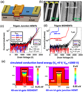
Figure 5. (a) Schematic of the NiO-based trigate GaN junction HEMT. (b) Scanning electron microscopy (SEM) images of the fin region before and after NiO sputter. Off-state I–V curves of the (c) trigate junction HEMTs and (d) trigate MIS-HEMTs with fin length of 200 nm, 500 nm and 1 µm. (e) Simulated potential barriers in a 40 nm trigate MIS-HEMT and 60 nm trigate junction HEMT at 1000 V VD and zero VG, revealing a lower barrier in a MIS trigate even with a smaller WFin. Reprinted from [56], with the permission of AIP Publishing.
Download figure:
Standard image High-resolution image3.2. Vertical power FinFETs
In 2016–2017, Sun et al reported the first E-mode vertical GaN power Fin-MOSFETs [32, 94] with a WFin of 450 nm, a Ron of 0.36 mΩ cm2 (normalized to the fin area) and a BV over 800 V. The major challenges to further improve the BV and Ron were found to be the E-field crowding at the fin corners and the high contact resistance at the top of sub-micron-meter fins, respectively. To address the first challenge, a wet-etch based corner rounding process was developed, which allows removal of surface dry-etch damages and rounding the sharp fin corners [95]. At the same time, a thick field oxide was inserted between the gate metal and trench bottom, which enables a reduced-surface-field structure that moves the peak E-field from the trench bottom to the device periphery [32, 33]. To address the second challenge, a highly-doped n+-cap-layer was added to the epitaxial structure, and a Cl-based treatment was applied to facilitate the Ohmic formation [33, 96]. With these optimizations, Zhang and Sun et al demonstrated 1200 V E-mode vertical GaN Fin-MOSFETs with 200 nm WFin and 1 mΩ cm2
Ron normalized to the total device active area [33]. This device shows one of the highest static power FOMs ( ) reported in all 0.6–1.7 kV Si, SiC and GaN transistors [33].
Subsequently, large-area 1.2 kV, 5 A GaN Fin-MOSFETs with a chip area of 0.45 mm2 were reported based on a 2 inch wafer fabrication process [34]. As shown in figure 6, the large-area device has about 700 fins and an implanted edge termination at the device periphery. The demonstration of large-area devices allows experimental evaluation of junction capacitances, which often do not scale with the area. The gate charge (QG) and gate-to-drain charge (QGD) were further derived, which usually determines the device switching loss in hard-switching applications. A record-high switching FOM [Ron·(QG + QGD)] in all 0.9–1.2 kV transistors was reported from the large-area vertical GaN FinFETs [34].
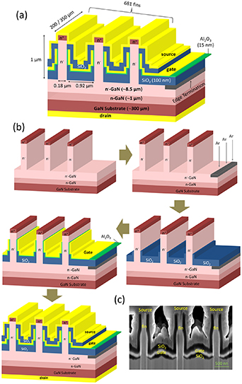
Figure 6. (a) Schematic of the large-area 1.2 kV, 5 A vertical GaN power FinFETs [34]. (b) Schematic of the main steps of the fabrication process of the large-area vertical GaN power FinFETs and the cross-sectional SEM images of the fin region [34, 41]. Reprinted with permission from [34, 41], © (2019, 2020) IEEE.
Download figure:
Standard image High-resolution imageWhile the fabrication of lateral GaN trigate HEMTs simply adds one or two steps for fin etch onto the standard HEMT process, the fabrication of vertical Fin-MOSFET is entirely different. As shown in figure 6, the fabrication starts with over 1 µm fin etch on the n+-GaN/n−-GaN epistructure, followed by corner rounding [95] and edge termination implantation [97, 98]. Then all dielectric and metal layers are fabricated in a bottom-up manner, starting from the conformal deposition or sputtering, followed by a controlled etch to the desired level. The accurate control over the etch depth of the sidewall-covering dielectric/metal layers is realized by a photoresist planarization and timed etch technique, where the etch-stop level is defined by the thickness of the remaining photoresist in sub-micron trenches [32, 33, 41].
The concept of vertical GaN Fin-JFET was first patented in [99], followed by the simulation presented in [66] and [67]. The trade-off between vertical Fin-JFET and Fin-MOSFET is similar to the one between lateral trigate MIS-HEMTs and trigate junction HEMTs [56]. The stronger depletion of the p–n junction can potentially allow the realization of E-mode operation with a less scaled fin width and the suppression of punch-through at high blocking voltages. In addition, by placing p-GaN close to the E-field crowding region at the fin corners, avalanche breakdown can be potentially realized without complicated E-field management structures. Whereas, the Fin-JFET channel only has the bulk fin conduction path; the absence of the sidewall MOS channels in parallel would increase the channel resistance when compared to the Fin-MOSFET channel [41].
As shown in figure 7(a), selective-area lateral p–n junctions were demonstrated by Yeluri et al [100] and Zhang [101] using the dielectric-masked p-GaN trench-filling regrowth, as well as by selective ion implantation by Tadjer et al [102] and Zhang et al [103]. Subsequently, initial experimental demonstrations of vertical GaN Fin-JFETs were reported by Kotzea et al [67] and Yang et al [104] by using the selective p-GaN regrowth (figure 7(b)) and the blanket-regrowth-then-planarization-etch approach (figure 7(c)), respectively. However, the Fin-JFETs fabricated in both works showed merely basic transistor behaviors with large off-state leakage currents, minimal voltage blocking capabilities, and an on/off current ratio below 100. The large parasitic leakage was reported to be located at the regrown sidewall p–n junctions. The origin of the leakage current in these regrown nonplanar p-GaN structures has been recently revealed [105], as being related to the n+-type interfacial impurities (e.g. Si, O, C) introduced in the regrowth process [106–112].
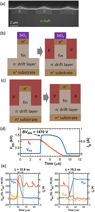
Figure 7. (a) Cross-sectional SEM images of the selective-area lateral p–n junctions by p-GaN trench-filling regrowth [101]. Schematic of the (b) dielectrics-masked selective-area p-GaN regrowth and the (c) blanket p-GaN regrowth and planarization for the Fin-JFET fabrication. (d) Avalanche waveform of the vertical GaN Fin-JFET in unclamped inductive switching. (e) 600 V/4 A turn-on/off waveforms in a double pulse setup with inductive loads, showing ∼10 ns rise time.
Download figure:
Standard image High-resolution imageVery recently in the 2020 IEEE International Electron Devices Meeting (IEDM), the first 1.2 kV vertical GaN Fin-JFET was announced by NexGen Power Systems and Virginia Tech [36, 37]. The Fin-JFET was fabricated by NexGen in a 100 mm GaN-on-GaN fab, and it shows an on/off current ratio of 109, a specific Ron of 0.82 mΩ cm2, an on-state current over 4 A, and a VTH as high as 2.05 V [37]. The VTH shows less than 0.15 V shift from 25 °C to 200 °C, revealing the robust normally-off operation. The specific Ron is found be to at least 3 ∼ 4-fold lower than commercial 1.2 kV SiC MSOFETs [37].
In addition, the 1.2 kV vertical GaN Fin-JFETs also shows a robust avalanche under the unclamped inductive switching conditions with an avalanche BV of 1470 V and an avalanche current over 1 A [36, 37] (figure 7(d)). Despite the earlier reports of avalanche in vertical GaN p–n diodes [113, 114], the vertical GaN Fin-JFETs demonstrated the first avalanche capability in GaN transistors to date. Double-pulse tests were also reported to evaluate the device switching performance. When switched at 600 V/4 A, a rise/fall time of 12.9 ns/10.3 ns and a total loss of 37 μJ were presented (figure 7(e)), which outperform the commercial SiC MOSFETs under similar switching conditions.
3.3. Comparison and benchmark
Table 2 benchmarks the key device metrics of the reported D-mode and E-mode lateral GaN FinFETs and trigate HEMTs, as well as the E-mode vertical GaN FinFETs, all for power switching applications. Figure 8 plots the BV vs. Ron trade-off of the E-mode FinFETs and trigate HEMTs, in comparison to other E-mode lateral and vertical power transistors. Generally, lateral GaN trigate HEMTs and vertical GaN FinFETs show superior performance over other similarly-rated devices (e.g. commercial planar HEMTs, vertical MOSFETs), reinforcing their potential for power applications.
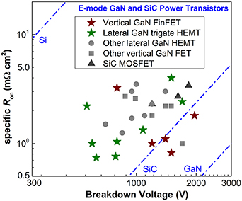
Figure 8. Ron vs. BV trade-off of the reported E-mode lateral GaN trigate HEMTs and vertical GaN power FinFETs, in comparison with other E-mode GaN and SiC power transistors.
Download figure:
Standard image High-resolution imageTable 2. Comparison of key metrics of the reported GaN FinFETs and trigate HEMTs for power applications.
| Device type | Reference | Device technologies | Year | WFin (nm) | On-off ratio | VTH a (V) | SS (mV dec−1) | Ron (Ω mm) | Specific Ron b (mΩ cm2) | BV (V) c @1 µA mm−1 | Destructive BV (V) |
|---|---|---|---|---|---|---|---|---|---|---|---|
| D-mode lateral FinFETs and trigate HEMTs | [52] | Schottky-type trigate | 2009 | 70 | 5 × 10⁵ | −3.5 | 110 | 17.2 | 12.5 | <10 | 250 |
| [82] | Heterojunction-free GaN FinFET | 2013 | 60 | 108 | −1.5 | 68 | 9.1 | 2.7 | ∼50 | 600 | |
| [84] | MIS trigate | 2017 | 150 | 1.5 × 10⁹ | −6.2 | 93 ± 7 | 9 | 0.91 | 792 | 792 | |
| [85] | MIS slanted trigate | 2017 | 350–700 | 109 | −2 | N/A | 9.4 | 1.52 | 1350 | 1350 | |
| [86] | Multi-channel MIS slanted trigate | 2019 | 50–100 | 109 | −3.5 | N/A | 2.8 | 0.47 | ∼350 | ∼1230 | |
| E-mode lateral trigate HEMTs | [80] | MIS trigate + AlGaN recess | 2012 | 120 | 108 | 0.53 | 86 ± 9 | 13.8 | 2.2 | 565 | 565 |
| [88] | MIS fin + planar gate with high WF gate metal | 2019 | 20 | 1010 | 0.6 | 110 | 10 | 1.33 | 1080 | N/A | |
| [89] | MIS trigate + AlGaN recess | 2019 | 200 | 109 | 1.4 | 95 ± 3 | 8 | 2.42 | 1700 | 2100 | |
| [90] | MIS trigate + InAlN recess | 2019 | 150 | 109–1010 | 2.3 | 65 | 8.65 | 1.04 | 800 | 800 | |
| [91] | MIS trigate + InAlN recess + Schottky-drain extension | 2020 | 225 | 1010 | 0.9 | 67 | 5.66 | 0.74 | 630 | 630 | |
| [92] | MIS trigate + trap charge gate oxide | 2019 | 100 | 108 | 2.6 | 73 | 5 | 0.76 | 788 | ∼1000 | |
| [56] | NiO-based junction trigate | 2020 | 60 | 108 | 0.45 | 63 ± 2 | 9.4–15 | 1.0–4 | 600–1500 | 600–2200 | |
| E-mode vertical FinFETs | [32] | Vertical Fin-MOSFETs | 2017 | 450 | 1011 | 1 | 75 | N/A | 3.24 | 800 V with 10−4 A cm−2 | |
| [33] | Vertical Fin-MOSFETs | 2017 | 200 | 1010 | 1 | 77 | N/A | 1.0 | 1200 V with 10−4 A cm−2 | ||
| [34] | 5 A large-area vertical Fin-MOSFETs | 2019 | 180 | 109–1010 | 1.3 | N/A | N/A | 2.1 | 1300 V with ∼µA | ||
| [36] | 4 A large-area vertical Fin-JFETs | 2020 | N/A | 109 | 2 [37] | N/A | N/A | 0.82 | 1470 V avalanche BV | ||
a Extracted at a drain current of 1 µA mm−1. b A gate-to-source of 1 µm is used in case that it is not reported; a transfer length of 1.5 µm is added for both source and drain contact in lateral devices. c BV extracted at a drain leakage current of 1 µAmm−1.
E-mode lateral GaN trigate HEMTs show excellent Ron vs. BV trade-off in the 600–1200 V range, while vertical GaN FinFETs exhibit superior performance at 1200 V level. Whereas, it should be noted that all the reported lateral GaN trigate power HEMTs are small-area devices, where the specific Ron calculation accounts for only about 1.5 µm transfer length for source and drain contacts (or completely ignored in some reports). Due to a possible larger finger width (over 3 µm) and other unaccounted areas in multi-finger HEMTs, the specific Ron of large-area [115] and commercial GaN HEMTs are often larger than the one of the small-area counterpart. In contrast, large-area vertical GaN FinFETs have been demonstrated [34, 36] and their switching performance have been studied in the context of power converters.
The lack of demonstration of large-area lateral trigate HEMTs makes it difficult to evaluate their capacitance, charges, and losses similar to the switching performance analysis and characterizations reported for vertical GaN FinFETs [34, 36, 116, 117]. Hence, at this moment, it is still not clear whether trigate HEMTs or vertical FinFETs would be more advantageous for 600–1200 V applications.
4. GaN FinFETs and trigate devices for RF applications
4.1. Lateral RF FinFET and trigate HEMTs
One of the primary challenges for large-signal RF applications of GaN transistors is the nonlinear behavior of short-channel devices. Figure 9(a) shows the gm characteristics of an ideal MOSFET, which increases linearly beyond VTH and remains flat after reaching the peak value. However, in conventional planar GaN transistors, gm shows distorted bell-shaped characteristics after reaching the peak value. This sharp gm drop causes a sharp drop in fT (figure 9(b)) and introduces non-linearity in large-signal operation. The device non-linearities result in significant side-bands, a saturation of output power at high input powers, as well as signal distortion in power amplifier operations. This issue becomes more serious as the gate length scales down. A relatively flatter gm characteristic is desirable for the linear large signal operation of GaN transistors. Several material-level (e.g. N-polar GaN [118], polarization engineering [119]) and circuit-level (derivative superposition and cancellation [120]) approaches have been proposed and demonstrated to improve the linearity of GaN transistors. However, the material-level and circuit-level approaches are challenging and create additional complexity. GaN NW or FinFET devices emerged as one of the most promising candidates for linear large-signal operation for the ease of technological implementation and tunability [23–25].

Figure 9. (a) gm of an ideal MOSFET and conventional planar GaN FET. GaN FETs show gm roll-off that causes non-linearity in large-signal operation. (b) fT of a planar GaN FET as a function of VGS. The fT profile resembles the gm roll-off which limits the high voltage operation at high frequency. Adapted and reprinted with permission from [25]. Copyright (2020) American Chemical Society.
Download figure:
Standard image High-resolution imageThe first high-frequency characterization of GaN NW FET was demonstrated by Vandenbrouck et al in 2009 [121], using a GaN/AlN/AlGaN MISFET structure. NWs were synthesized on a c-plane sapphire substrate, with 80–160 nm diameter and 10–20 μm length. Maximum transconductance (gm,max) value of 45 μS with relatively flat gm profile over 5 V was demonstrated. The device also showed an fT of 5 GHz. Despite the promising performance, the bottom-up technology for NW formation limits the device scalability (only 5 NWs in [121]) for applications. Moreover, the demonstrated device also suffers from low current driving capability [47].
To overcome the challenges of bottom-up technology, Azize et al [47] demonstrated NR MIS-HEMTs by top-down selective etching of InAlN barrier layers on GaN. A conformal Al2O3 layer was deposited in InAlN/GaN NRs to both increase the NR charge density through piezoelectric-induced doping and reduce the gate leakage current. The devices with Wfin of 50–90 nm showed gm,max of 15 mS with relatively flat profile over 5 V. fT of 6.75 GHz and fmax of 14.5 GHz were measured. In this device, multiple NRs are formed in parallel between source and drain, which may potentially increase the source access resistance due to limited source contact area [23].
There have been several explanations for the gm roll-off in the literature, including self-heating effects [122], an increase of the dynamic source access resistance [123], emission of optical phonons [124], and contact barriers [125]. Lee et al [23] proposed that suppression of source access resistance can improve the gm roll-off behavior in GaN NW HEMTs and demonstrated InAlN/AlN barrier HEMTs where NWs were only formed under the gate region while maintaining planar structure under the source region (figure 10(a)) to enable higher current injection to the channel [23]. The highly scaled (gate length LG = 70–80 nm, Wfin = 88 nm) devices showed superior current driving capability (3.5 A mm−1 at VG = 1 V), suppression of gm and fT roll-off at higher biases compared to the planar HEMTs (figure 10(b)). A peak fT of 100 GHz was demonstrated, which is 35% lower than planar devices due to fringing capacitances from the side gate and access region that are wider than the effective channel region [23].

Figure 10. (a) Schematic and the top view SEM image of the NW channel trigate HEMT. (b) Comparison of DC transfer characteristics of NW channel device with planar device. Reprinted with permission from [23], © (2013) IEEE.
Download figure:
Standard image High-resolution imageTo improve the gm roll-off suppression characteristics, Jo et al [126] found that the crystal selective wet etch can improve the sidewall morphology by mitigating the plasma etch damages and hence, increase the contribution of sidewall MOS channel. The positive VTH of the sidewall MOS channel, along with the negative VTH of the 2DEG channel, can suppress the gm roll-off and enable broad gm-plateau [126]. Moreover, different plasma (fluorine, O2, N2O) treatments [127, 128] and self-aligned [129] gate technology can be used to improve the frequency performance and current driving capability of these devices.
Ture et al [130] demonstrated the use of the quaternary InAlGaN and binary AlN barrier layers lattice-matched with AlN spacer to improve the saturation ID and gm of trigate HEMTs when compared to the AlGaN-based counterparts [130]. The high Al-concentration InAlGaN and AlN barrier can offer larger polarization difference with GaN and hence, higher 2DEG density [22] and higher ID,max (3.8 A mm−1 for AlN compared to 2 A mm−1 for AlGaN). In 2017, Ture et al demonstrated a four stage W-band power amplifier using AlN barrier trigate HEMTs for the first time [131]. The power amplifier using trigate devices shows superior output power, gain, and power added efficiency (30 dBm, 12 dB, 6%, respectively) over planar devices (28 dBm, 10 dB, 4%, respectively) in the frequency range of 86–94 GHz [131].
In 2017, Zhang et al [132] first reported the improvement of linearity in large-signal operation due to the suppression of gm roll-off using T-gate AlGaN barrier trigate HEMT. An on-wafer load-pull measurement at 8 GHz (class AB operation with VD = 28 V, ID,Q = 0.1 ID,max) showed output power Pout = 11.3 W mm−1 (1.66 × higher than planar HEMTs). The Pout enhancement was attributed to the combination of ID improvement and self-heating suppression in trigate device [132]. The third order inter-modulation distortion (IM3) of FinFET showed a ∼5.5 dBc improvement over a planar device, which is aligned with the suppression of gm roll-off.
To further improve the linearity performance of GaN trigate devices, Joglekar and Radhakrishna et al [24]. proposed and demonstrated a device-level analog of the circuit-level 'gm compensation' technique using a composite device consisting of multiple fins with variable widths. The key idea is to minimize IM3, which is proportional to the second derivative of gm, i.e.  . A carefully designed composite device with multiple parallel fins with variable width (different VTH) can cancel out
  (figure 11(a)) and lead to a highly linear transistor with very low IM3. Class AB operation of a composite AlGaN barrier device containing five different WFin (ranging from ∼150–450 nm) shows a significantly higher Pout at 6 GHz with no saturation for input power Pin up to 15 dBm, delayed onset of second and third harmonic, and 20 dB reduction of IM3 compared to the planar device. A significant reduction in second harmonic (and hence delayed gain compression) is consistent with the fact that the flat-gm characteristics lead to
  0 [24]. However, due to the presence of multiple VTH's in the device, the conduction through the lower VTH fins can create non-linearity in the composite device current at higher VG. Moreover, the width of the gm-plateau cannot be substantially improved for large-signal operations with Fin only architectures (due to limited tunability range for VTH) and Schottky metal gates (which are susceptible to gate diode turn-on and large leakages at small positive VG) [25].

Figure 11. (a) Illustration of device-level gm-compensation principle: g''m for a set of five independent transistors with slight (0.2–0.3 V) offsets in VTH (left). When these transistors are connected (right), the composite g''m (black curve) is lowered (b) schematic diagram and top view SEM image of two different types of composite devices demonstrated in [25] with fins of different widths between the source and drain. (c) Top-view SEM images of the composite device demonstrated in [25] showing a planar region and a fin region under a single gate electrode. (a), (b) Reprinted with permission from [24], © (2017) IEEE. (c) Reprinted with permission from [25]. Copyright (2020) American Chemical Society.
Download figure:
Standard image High-resolution imageTo overcome these challenges, Choi et al [25] adopted a composite MIS-HEMT where the channel is a combination of both planar HEMT and fins with different widths [25], as shown in figure 11(b). The use of the MIS structure allowed a wider range (−0.5 to −4 V) of VTH tunability. With careful optimization of fin width and number of fins along with T-gate, a composite device with gm-plateau > 6 V, and  ≈ 0 in four different VG values has been demonstrated. Single-tone measurement of the device showed a maximum power-added efficiency (PAE) of 32.3%, and two-tone measurement at 30 GHz showed 3rd order output intercept point (OIP3) and OIP3/PDC of 31 dBm and 8.2 dB, respectively. The high linearity and low noise FOM show the promise of the composite device in mm-wave low noise amplifier application over 20 GHz [25].
Another interesting trigate device structure that can offer high linearity in GaN power amplifier is superlattice castellated FET (SLCFET), which was originally proposed for RF switching applications [133–136]. The superlattice channel of the device consists of stacked 2DEG layers similar to the multi-channel structure shown in figure 1, where the trigate structure is essential for electrostatic control of the buried 2DEG layers. It should be noted this SLCFET predates the multi-2DEG-channel trigate HEMTs later developed for power applications [86, 87]. Due to the presence of multiple channels in SLCFET, gm shows unique double hump and broad plateau characteristics, which lead to higher linearity. Recently, LG = 150 nm T-gate SLCFET with fT = 47 GHz, fmax = 124 GHz, Pout >6 W mm−1, PAE >45%, and OIP3/PDC = 6 dB at 30 GHz using large-signal measurement have been demonstrated in the second-generation GaN SLCFETs [134].
A planar nano-strip channel structure has been proposed by Xing et al by using partial ion implantation isolation to define fin-like channels under the gate [137]. This structure overcomes the parasitic capacitance issue caused by the gate metals on the fin sidewalls. InAlN/GaN GaN HEMTs with a gate length of 80 nm were reported, with both wrapped-gate fin channels and planar nano-strip channels. The planar-nanostrip-channel HEMTs showed a roughly constant source resistance at different ID's as well as much flatter gm and fT than those in planar HEMTs, as well as an fT higher than that of standard Fin-HEMTs. Later, Xing et al introduced an MIS gate to reduce the gate leakage current and further increase the device's linearity [138].
In addition to linearity improvement, the trigate structure was also used to make E-mode RF HEMTs. Liu et al reported the E-mode Schottky-type trigate HEMTs with WFin below 90 nm [55]. However, the reported fT and fmax are relatively low due to the large gate length (2 µm) in the fabricated devices.
4.2. Vertical RF FinFET
In 2020, Perozek et al [139] adapted the vertical FinFETs in [32, 34, 94] for use in RF applications. Key design modifications include the use of a highly-insulating substrate instead of bulk-GaN, capacitance reduction, and gate length scaling. Due to the tightened dimensional tolerances of a scaled device, new techniques were necessary for the gate etch and spacer fabrication. Both steps utilize an oxide planarization technique to ensure a high degree of uniformity across the device before performing an etch-back step for vertical patterning. A cross-sectional schematic and SEM image is shown in figure 12. On-wafer RF characterization is made possible by a top-side drain contact. To date, only small-signal data is available with a reported fT of 5.7 GHz and fmax of 2.8 GHz, although further work is claimed to be necessary for optimized power-handling capabilities.
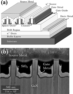
Figure 12. (a) Cross-sectional schematic of the GaN quasi-vertical RF FinFET. (b) SEM cross-section of the fabricated device [139].
Download figure:
Standard image High-resolution image4.3. Comparison and benchmark
Table 3 compares the main device metrics of GaN lateral trigate HEMTs and vertical FinFETs for RF and large-signal applications. There have been a significant number of reports on the gm roll-off suppression and small-signal frequency performance improvements. However, there are only a few reports on the large-signal characterization. Figure 13 shows the evolution of fT, fmax and gm,max as a function of the gate length for different barriers. Aggressive Lg scaling, high Al-concentration barrier, and advanced gate technology (e.g. T-gate) are essential to extend the frequency limits of these devices.
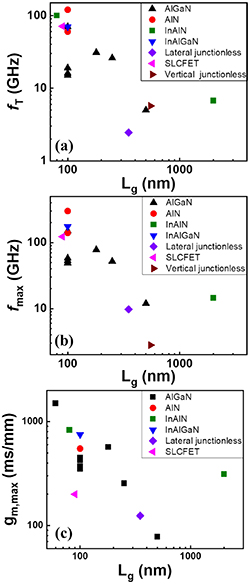
Figure 13. (a) Evolution of fT, (b) fmax, and (c) gm of GaN trigate and FinFET devices as function of gate length.
Download figure:
Standard image High-resolution imageTable 3. Comparison of key metrics of the reported GaN FinFETs and trigate HEMTs for RF applications.
| Device type | Reference | Barrier | Year | WFin (nm) | Lg (nm) | fT (GHZ) | fmax (GHz) | gm ,max (mS mm−1 ) | ID,max (A mm−1 ) | PAE (%) | OIP3 (dBm) |
|---|---|---|---|---|---|---|---|---|---|---|---|
| Lateral FinFETs and trigate HEMTs | [121] | AlN/AlGaN | 2009 | 80 | 500 | 5 | 12 | 78 | 0.87 | N/A | |
| [47] | InAlN | 2011 | 50–90 | 2000 | 6.75 | 14.5 | 312 | 2.9 | |||
| [23] | InAlN/AlN | 2013 | 88 | 80 | 100 | N/A | 830 | 3.5 | |||
| [140] | Junctionless | 2014 | 200 | 350 | 2.45 | 9.75 | 124 | 0.4 | |||
| [130] | AlGaN | 2016 | 100 | 100 | 70 | 150 | 370 | 2 | |||
| InAlGaN | 70 | 175 | 750 | 2.1 | |||||||
| AlN | 60 | 140 | 550 | 3.8 | |||||||
| [129] | AlGaN | 2017 | 300 | 60 | 55 | 140 | 1500 | 1.3 | |||
| [127] | AlGaN | 2017 | 100 | 180 | 16 | 53 | 351 | 0.708 | |||
| 15 | 49 | 424 | 0.6 | ||||||||
| 19 | 58 | 450 | 0.61 | ||||||||
| [131] | AlN | 2017 | 200 | 100 | 120 | 300 | 550 | 1.9 | |||
| [132] | AlGaN | 2017 | 152 | 180 | 31 | 78 | 570 | 1.64 | 53 | N/A | |
| [24] | AlGaN | 2017 | 150–450 | 250 | 26 | 52 | 255 | 0.75 | N/A | 36 | |
| [134] | AlGaN/GaN superlattice | 2019 | N/A | 150 | 47 | 124 | 175 | 1.8 | 45 | N/A | |
| [25] | AlGaN | 2020 | 50–160 | 90 | 71 | 123 | ∼200 | 1.6 | 32.3 | 31 | |
| Vertical Fin-MOSFETs | [139] | Junctionless | 2020 | 80 | 550 | 5.7 | 2.8 | 17.4 kS cm−2 a | 15 kA cm−2 a | N/A | |
a In vertical FinFET devices, gm and ID are normalized using the total active area which includes both fin footprint and the spacing between the fins.
5. Modeling and physical studies
Numerous simulations and analytical models have been developed for Si digital and microwave FinFETs [141–147]. However, lateral GaN trigate HEMTs differ from Si FinFETs due to the 2DEG channel which is not present in conventional bulk FinFETs. For example, the interplay between the 2DEG channel and the sidewall MOS channel in the MIS-type trigate HEMTs has been found to induce strong nonlinear dependence of device characteristics on WFin [148].
On the other hand, vertical GaN power FinFETs also differs from the conventional power MOSFETs and insulated-gate bipolar transistor (IGBTs). For example, the leakage current and breakdown are determined by p–n junctions in MOSFETs and IGBTs; however, vertical Fin-MOSFETs are junctionless and the relevant leakage and breakdown mechanisms are expected to be significantly different [41].
These differences with Si FinFETs have motivated the simulation and modeling works for GaN FinFETs. The aim of this section is to provide a comprehensive review of the modeling studies and physical analysis of lateral trigate HEMTs and vertical FinFETs. The presented device physics can provide critical design guidelines that correlate device parameters to performance metrics.
5.1. Lateral trigate power HEMTs
VTH is of paramount importance for trigate GaN HEMTs, particularly for power applications where the E-mode operation is essential. Alsharef et al present one of the earliest theoretical investigations of the VTH in Schottky-type trigate HEMTs [17], taking into account the sidewall Schottky-gate depletion and partial strain relaxation. The work also provided guidelines on choosing material properties to enable a VTH positive shift with the increased WFin.
In trigate GaN MIS-HEMTs, the impact of the fin-sidewall MOS channels is crucial to device characteristics. The accumulation-mode sidewall MOS channel is inherently E-mode; however, if donor-like traps and fixed charges are introduced in the fabrication, it could become D-mode. Takashima et al reported that, without a post-etch treatment in the process, the fabricated trigate MIS-HEMTs show a lower VTH than planar HEMTs, and their I–V characteristics are dominated by the D-mode sidewall MOS channels [149]. Son et al reported that the acceptor-like MOS traps, although leading to positive VTH shift, but induce significantly worse SS [150]. These results suggest the importance of optimizing the fin etch and post-treatment processes to enable E-mode, high-performance trigate MIS-HEMTs.
Compact models for trigate GaN MIS-HEMTs have also been reported. Yadav et al presented a macro model that captures the parallel 2DEG and sidewall channel conductions as well as the strongly nonlinear WFin dependency on device characteristics [148]. A more complete set of physical models were reported by Ren et al [151], which correlate VTH and on-state saturation current to device design parameters.
A limitation of the above models is the limited description of the off-state characteristics. In fact, physical models for device BV and off-state leakage current are still lacking. The critical role of the potential barrier height in the 2DEG fin on the device leakage current was initially studied in [56]. The lowest barrier was found to locate at the middle of the fin in the 2DEG plane, and the barrier height is determined by the trigate depletion. The barrier height was simulated in junction trigate and MIS trigate using 3D technology computer-aided design (TCAD) simulation, and it was used to explain the different off-state leakage current and BV in trigate junction HEMTs and trigate MIS-HEMTs [56].
Trigate structures have also been reported to alleviate the current collapse and dynamic Ron issues in GaN HEMTs, which is beneficial to both RF and power applications. An early study on the unpassivated Schottky-type trigate HEMTs reported the current collapse reduction, which was attributed to the reduce E-field crowding at the gate edge [53]. The dynamic characteristics of a Fin-MIS-HEMT were studied in [18], where the reduced current collapse was attributed to the lower gate leakage current and smaller VTH shift. A recent dynamic Ron study was presented by Ren et al [19] for a trigate MIS-HEMT. It was found that the trigate device shows reduced Ron degradation due to the reduced E-field crowding as well as the faster Ron recovery owing to the quick electron emission assisted by the shallow sidewall traps [19]. Despite these encouraging results, it should be noted that the above devices are all D-mode and do not possess the gate field plates that are widely used in commercial devices; the impact of trigate structures on device dynamic performance needs to be further studied in E-mode devices with good passivation.
5.2. Lateral RF FinFETs and trigate HEMTs
Alsharef et al [22] and Zhang et al [152] studied the design space of the fin geometry in lateral trigate GaN HEMTs for optimum RF performances using numerical and TCAD simulations, respectively. Simulations show that fT and fmax of the planar device are superior over a wide range of LG. The trigate designs exhibit smaller output transconductance (gds) than planar HEMTs, which is a sign of better electrostatic integrity at the expense of higher gate-to-source capacitance (CGS). The origin of higher CGS can be attributed to the larger intrinsic and fringing capacitances. Careful geometric optimization can maximize the RF performance and surpass planar HEMTs by minimizing CGS while maintaining gds. CGS can be minimized by reducing the fin height and fin spacing and increasing the fin width. The narrower fin can increase gm due to enhanced gate control [153], but it can also deteriorate the linearity [152]. The reduction of fin height may lead to lower gm and higher gds, which are detrimental to RF performance. Alternatively, lower CGS can be achieved using SiNx sidewall passivation [22].
Several groups [140, 152, 154] subsequently used small-signal equivalent circuit modeling to understand the RF performance of GaN trigate/FinFET devices. Gate parasitics extracted at high VDS suggest that increasing VG has minimal effect on CGS of planar FETs, leading to a continuous decreasing trend of fT with a high slope. Whereas for trigate case, sharper reductions in CGS have successfully been obtained in Fin-FETs with shorter fin length (LFin). Moreover, the reduction of Lfin can lower the extrinsic resistances and the peak value of intrinsic transconductance, as well as improve fT and fmax [152]. The capacitance reduction, accompanied by flatter gm, enables an fT boosting and makes it more uniform over VG. Compared to planar HEMTs, the influences of trigate CGS were also discovered to be more predominant than the ones of CGD with higher ratios between on-state and off-state capacitances. In addition, the influence of trigate channels on CDS is not critical, whereas the gds strongly depends on the LFin with a declining trend [154].
Compact models (e.g. MIT virtual source GaN FET [24]) calibrated against experimental devices have been used by Joglekar and Radhakrishna et al [24] to evaluate the linearity performance of the composite device. According to the modeling, the VTH-engineering-aided gm-compensation technique in an optimized commercial GaN HEMT can potentially yield highly linear RF GaN HEMTs with low signal distortion. These results emphasize the potential of GaN-technology in advanced high-power and high-frequency RF applications [24].
5.3. Vertical power FinFETs
The junctionless vertical GaN Fin-MOSFETs possess very different device physics when compared to the conventional power MOSFETs, JFETs, bipolar junction transistors, and IGBTs. An in-detail tutorial has been provided in [41]. Here we provide a sketch of the interesting physics in vertical power Fin-MOSFETs.
The Ron components in vertical Fin-MOSFETs mainly consist of the source contact resistance, fin channel resistance, and drift region resistance, with a complete analytical model reported in [64]. In the fin channel, the current distribution between the bulk fin and the sidewall MOS channel strongly depends on VG, bulk fin doping, and mobility, as well as the accumulation MOS mobility and unit capacitance. In the drift region, the current spreading needs to be considered when calculating its resistance. In experimental 1.2 kV GaN Fin-MOSFETs, the drift region was found to be the major contributor in device Ron, followed by the source contact resistance on fins and the fin channel resistance [64].
The leakage and breakdown of vertical Fin-MOSFETs are mainly determined by the potential barrier in the fin channel, which controls the carrier supply, as well as the carrier transport in the thick and lightly-doped drift region [98]. When the potential barrier is sufficiently high, the leakage is very low, and device BV is limited by the peak E-field in the edge termination region. When the potential barrier is low, a lower device BV could be triggered by high leakage current that is related to carrier transport. The leakage current in the drift region is usually dominated by the Poole Frenkel emission [37, 113] or the variable range hopping through dislocations [74, 155]. If the barrier is further lowered at high drain voltage, a large amount of injected electrons are trapped in the drift region and induce space-charge-limited conduction (SCLC), leading to a trap-mediated breakdown [98, 113]. This SCLC mechanism has also been widely reported in vertical GaN-on-Si devices [31, 71, 76, 79, 156].
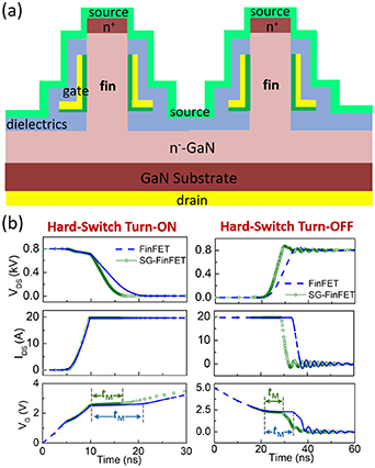
While the device parameters in the fin region determine the device Ron and BV, the inter-fin region was found to be critical to the device switching performance [116, 117]. In the high-voltage hard switching, the turn-on/turn-off losses are mainly determined by the Miller plateau duration (tM) when the entire drift region is discharged/charged. Wang et al proposed a split-gate structure, which removes the gate metal in the inter-fin region and exposes the drift layer to the field lines from the source metal (figure 14) [116, 117]. This structure allows a combination of drain-to-source current and gate current to (dis)charge the drift region and thus enables a much shorter tM. Device-circuit mixed-mode simulations predict 38% lower switching losses in 1.2 kV GaN power Fin-MOSFETs by using the spit-gate inter-fin design [117].
Figure 14. (a) Schematic of the split-gate vertical power FinFETs with gate stack removed in the inter-fin region. (b) Hard-switched turn-on and turn-off waveforms of a spit-gate FinFET and a standard FinFET from device-circuit mixed-mode TCAD simulation. Reprinted with permission from [117], © (2020) IEEE.
Download figure:
Standard image High-resolution image
6. Perspectives: current challenges and research opportunities
6.1. FinFETs and trigate HEMTs for power applications
Very recently, several companies started to commercialize the GaN FinFET and trigate HEMT technologies for power applications. For example, Cambridge Electronics Inc. is commercializing a 3D-GaN technology based on lateral trigate HEMTs [157]. NexGen Power Systems Inc. is commercializing the vertical GaN Fin-JFET technology [36, 37, 158]. The active technology transfers in this field suggest numerous research opportunities and high impact. Here we attempt to present a comprehensive perspective on the challenges and research opportunities for GaN power FinFETs and trigate HEMTs.
Before discussing the challenges facing each type of devices, we point out that a common gap for many GaN FinFETs and trigate HEMTs is their thermal management, which is critical for both power and RF applications. Excellent high-temperature characteristics have been reported in a few devices, including the lateral trigate GaN junction HEMTs [56], vertical GaN Fin-MOSFETs [33], and vertical Fin-JFETs [36, 37]. However, extensive thermal management studies are still lacking in fin-based GaN devices. Note that the device-level thermal management is expected to be tightly related to the device packaging. For example, if junction-cooling is enabled by the package, the fin pitch and interfin materials could be critical factors for device-level thermal performance. In contrast, if heat is extracted from the backside of the wafer, device architecture (e.g. lateral, vertical), substrate material, and chip thickness could matter more.
6.1.1. Lateral trigate power HEMTs.
Despite the good performance demonstrated in trigate HEMTs, more in-depth analyses are needed to identify their enabling capabilities and application spaces, particularly in comparison to the commercial 15–650 V E-mode HEMT technologies. All existing commercial HEMTs have a planar gate and realize E-mode operation mainly by two approaches: (a) using an E-mode HEMT with a p-GaN region under the gate that forms Ohmic or Schottky contact with the gate metal [38], or (b) co-packaging a D-mode HEMT with Si MOSFETs in a cascode circuit or other 'direct drive' configurations [14].
An advantage of the E-mode trigate technology that has not been made explicit until recently is the significantly lower channel resistance in the gate region. While the resistance of the access region is determined by the 2DEG sheet resistance, the 'sheet resistance' in the gate region (RSH_G) depends on the unit gate capacitance (CG), which determines the electron concentration at a given gate overdrive, as well as the channel mobility (µCH) [56]. In planar p-gate HEMT, the large distance between the gate metal and 2DEG renders very small CG and low electron concentration. In the gate-recess HEMT, the 2DEG channel is usually replaced by the MOS channel, which significantly degrades µCH. In comparison, the trigate retains the 2DEG channel and places gate metal close to the 2DEG channel, therefore allowing a much smaller RSH_G. The RSH_G of experimental E-mode trigate HEMTs was first calculated in [92]. Subsequently, [56] reported the calculated RSH_G for all the prior E-mode trigate HEMTs as well as the p-gate and recessed-gate HEMTs, revealing a generally 5 ∼ 10-fold lower RSH_G in E-mode trigate HEMTs compared to other E-mode technologies.
The significantly lower RSH_G supports the promise of E-mode trigate HEMTs for not only high-voltage power applications but also low-voltage power applications, as the channel resistance in the gate region has an increasing contribution to the total device Ron in lower-voltage devices. For example, E-mode power devices with BV from a few volts to tens of volts are in great demand in point-of-load converters (e.g. for 48 V–1 V power conversion in data centers) [159]. The promise of E-mode trigate HEMTs for low-voltage applications is further strengthened by the superior gate controllability, which allows aggressive scaling of gate length and the channel resistance in the gate region.
An open question associated with the application space of trigate HEMTs is the optimal trigate structure. In general, E-mode trigate HEMTs are more desirable than the D-mode counterparts. As can be seen in table 2, the WFin required for E-mode realization, which correlates to the lithography requirement and fabrication cost, varies among different trigate structures. The standard trigate MIS-HEMTs require WFin scaling down to 20–30 nm for E-mode realization. NiO-based trigate junction HEMTs and the charge trap oxide relax the scaling requirement to WFin of 60–100 nm. By adding a gate recess (see figure 3), 150–250 nm WFin is sufficient for E-mode realization, suggesting the device can be manufacturing in a 0.15 µm CMOS processing line. However, the recessed gate region may limit the gate length scaling and compromise RSH_G. These trade-offs imply the optimal trigate structure may depend on the target voltage class and application scenarios.
To evaluate the application space of various E-mode trigate HEMTs, another immediate need is to study their junction capacitances, charges, and switching losses by experiment, modeling, and simulation. To date, there are very few analyses on the switching performance of trigate GaN HEMTs. In contrast, switching-related parameters have been extensively studied in the newer vertical GaN FinFETs [34, 116, 117, 160]. A recent work looked into the capacitances and charges in D-mode trigate GaN MIS-HEMTs [161]. However, in E-mode trigate MIS-HEMTs, the turn-on of the E-mode sidewall MOS channels will complicate the analysis of junction capacitance, gate charges, and switching losses and may lead to different design trade-offs. In fact, the impact of the MOS conduction on device static and switching performance is a key open question for trigate GaN MIS-HEMTs. Broadly speaking, optimization of different E-mode trigate HEMTs should be further studied considering the potential trade-offs between device static and switching metrics under different power applications (e.g. hard-switching and soft-switching at different voltage levels).
6.1.2. Vertical power Fin-MOSFETs.
A perspective on the common challenges for wide-bandgap and ultra-wide-bandgap vertical power FinFETs has been provided in [41]. Here we focus on the challenges and opportunities specific to vertical GaN power Fin-MOSFETs.
An immediate need for advancing the performance of vertical GaN Fin-MOSFETs is to understand the physics, material science, and processing technologies regarding the electronic transport properties in the fin channel and the sidewall accumulation-mode MOS channel. A recent analysis has revealed that the fin channel mobility and MOS mobility in state-of-the-art 1200 V vertical GaN Fin-MOSFETs is much lower than the drift region mobility [64]. While a decade of studies has been performed on the MOS formed on planar AlGaN/GaN [162], the electron mobility, interface states, interface charges, and dynamic responses of the sidewall MOS formed on the etched non-polar GaN, as well as their correlations processing conditions and oxide materials, are far from being understood. Some immediate knowledge gaps to fill may include the physics of transport properties on m-plane and a-plane GaN sidewalls, the MOS interfacial properties, as well as the further optimization of dry etch and wet treatment processes. These studies are important not only for vertical Fin-MOSFETs but also for trigate MIS-HEMTs where the sidewall MOS channel can be turned on with 2DEG to lower the resistance in some device designs and applications.
The studies in [64] revealed that the sidewall MOS channel has a lower resistance than the bulk fin channel and therefore dominates the fin channel conduction when the FinFET is fully turned on. This suggests the potential benefits of using the trigate structure in vertical MOSFETs, in which the MOS gate stack wraps around the sub-micron vertical n-GaN pillars. This trigate vertical MOSFET can potentially have a lower channel resistance than that in vertical Fin-MOSFETs, further expanding the application space of vertical power MOSFETs to lower voltage classes (where the device Ron is increasingly contributed by the gate-modulated channel region). Similar trigate structures have also been recently proposed for the inversion-mode vertical SiC MOSFETs [163].
A common knowledge gap for vertical GaN Fin-MOSFETs and lateral GaN trigate MIS-HEMTs is the bias temperature stability, reliability, time-dependent dielectric breakdown, and ruggedness of gate oxide. Gate oxide reliability has been a key concern for planar lateral GaN HEMTs and SiC power MOSFETs; the relevant studies have continued for decades. Whereas, to date, there are still very few reports on the gate oxide reliability on sidewall nonpolar GaN, which is key to understand the gate reliability and ruggedness in FinFETs and trigate devices. Very early studies have looked into the degradation, dynamic Ron, and charge trapping in the first-generation vertical GaN Fin-MOSFETs [164–166], which manifest the necessities for extensive gate reliability studies for GaN FinFETs and trigate devices.
6.1.3. Vertical Fin-JFETs and trigate junction HEMTs.
In unipolar power devices, p–n junctions are highly desired as they can provide a stronger depletion than the MIS stack, avoid the possible oxide reliability issues, allow superior thermal stability, and potentially enable avalanche and surge ruggedness. An early demonstration of the trigate junction HEMTs using p-NiO/n-GaN heterogeneous p–n junctions has already shown many inherent advantages of the junction trigate when compared to the MIS trigate [56] (see figure 5). It was also envisioned in [56] that a homogenous GaN p–n junction could allow further performance advancements. This vision has been fulfilled in the 1.2 kV vertical GaN Fin-JFET, which has enabled one of the best trade-off between Ron and BV in 900–1700 V class power devices, as well as the robust avalanche and fast switching capabilities [36, 37].
The current challenge of developing high-performance trigate junction HEMTs and vertical JFETs using homogenous GaN p–n junctions is the immaturity of the selective-area p-type doping technique in GaN. As mentioned in section 3, the p-GaN regrowth on nonplanar n-GaN structures often lead to high leakage current and compromised blocking field at the regrown lateral p–n junction. Many papers have reported the mechanism of the leakage current across the regrown p–n junction [106–112], and a recent study by Xiao et al unveils the origin of the leakage current along the regrown p–n junction [105]. Many of these leakage currents were found to be related to the n+-type interfacial impurities introduced in the regrowth process as well as the dependence of growth dynamics on crystallographic orientations [105]. Despite the successful demonstration of the good-quality regrown p–n junctions by NexGen [36, 37], a universal approach to suppress the leakage current in the regrown GaN p–n junction on the nonplanar structures seem still lacking in the literature. Very recently, Xiao et al demonstrated the first p-GaN/2DEG junction with low leakage current and high E-field, by using a pre-Mg treatment in the regrowth to suppress the interfacial impurities [106]. This result has retired a key risk for demonstrating the p-GaN based trigate junction HEMTs.
P-type ion implantation is another pathway currently under extensive investigation for selective doping. The activation of implanted Mg ions in GaN was realized by multicycle rapid thermal annealing [102, 167–169], but the concentration is usually relatively low (∼1016 cm−3) [103]. Recently, Sakurai et al demonstrated the activation of >1018 cm−3 implanted Mg ions through ultra-high-pressure annealing [170]. This suggests good promise for making the implantation-based Fin-JFETs.
Finally, the successful selective-area doping in GaN can allow the realization of the superjunction (SJ) drift region, which can be integrated with the FinFET and trigate channels. Recently, an SJ-FinFET was proposed, in which one or multiple fin channels are placed on top of each n-type pillar in the SJ drift region [160, 171]. The combination of high-density fin channel and SJ drift region is predicted to far outperform the 1D GaN limit and provide excellent switching performance. The SJ-FinFET shows good promise for enabling multi-megahertz, multi-kilovolts power switching [160].
6.2. FinFETs and trigate HEMTs for RF applications
6.2.1. Lateral trigate RF HEMTs.
While the benefits of a trigate structure to facilitate gate length scaling and linearity enhancement are clear, the development of trigate RF HEMTs is still in a relatively early stage with future success relying on addressing key limitations in their fabrication and design.
Currently, the high-frequency performance of trigate devices lags far behind their planar counterparts. With some state-of-the-art planar HEMTs reaching 20 nm gate length with fmax in excess of 500 GHz [172] or others with Johnson's FOM of  [173], it is clear that there is much room for optimization within the FinFET design space. Currently, two major limitations are present: (a) high cost for LG and WFin scaling in the foundry process, and (b) increased parasitics due to inter-fin effects.
From the discussions in section 4, it can be seen that the demonstrated linearity enhancement in GaN trigate HEMTs often requires the smallest WFin below 150 nm. This poses a more demanding lithography requirement when compared to the 0.5 µm process for C-band RF applications and the 0.25 µm process for X-band RF applications, implying an increased fabrication cost. From the cost viewpoint, the commercialization of GaN RF trigate HEMTs may meet a lower barrier in milliwave and THz applications, where a short gate length <100 nm has to be used for planar HEMTs as well. In addition, a higher cost may incur when transferring the fin etch and post-etch treatment processes to the large-diameter foundry production lines and optimizing the process uniformity and reproducibility.
With all gate fin structures being three dimensional, an increase in gate metal periphery is unavoidable. Though the parasitic sidewall capacitances are relatively insignificant for power trigate devices (charges matter more), their impacts are much more pronounced in RF applications. The excess gate metal between fins increases the gate capacitance, causes signal delay, and therefore reduces fT and fmax [174]. While this issue can be minimized by shallow etches and reduced fin-to-fin pitch, by decreasing the pitch between fins by too much, the device may behave similarly to a planar device where the increase in source access resistance at high biases reduces the device's linearity [23].
To address the above issues, novel fin-gate structures that allow superior trade-offs between gate controllability and parasitic capacitance would be highly desirable. The planar-nanostrip channel could be a potential route to explore, but the implantation-based isolation used in [137] is not ideal as the isolation weakens the sidewall gate modulation. A planar-nanostrip structure with fin channels separated by p-type materials can be potentially superior. In the meantime, the recently-demonstrated junction trigate [56] may also see advantages for RF devices. The junction sidewall stack provides stronger gate controllability when compared to the MIS gate, and at the same time, significantly reduces the parasitic sidewall capacitance.
Another immediate need for RF FinFETs and trigate HEMTs is a comprehensive analysis and benchmark between different structures. Currently, fair comparisons between device structures reported in the literature are hindered by non-standardized normalization methods for devices and unreported key dimensions. Commonly, the area is computed as the source-to-drain distance times the width of the active region beneath the gate. While the current typically scales with this effective gate width, it ignores the space etched between each gate fin and hides benefits from reduced source/drain access resistances. Moreover, total gate length, including the inactive regions, is necessary for comparing wafer costs, heat dissipation, gate capacitance, and power density.
As many planar HEMTs begin to see a saturation in output current, a shift towards multi-channel structures looks promising. These devices, which stack multiple 2DEGs for reduced sheet resistance, struggle from poor pinch-off because the upper channels shield the effect of the gate from the lower channels [175]. Devices such as the SLCFET have utilized a trigate design to simultaneously pinch off multiple channels laterally [123, 125, 160]. Another potential advantage of the multi-channel devices is that the device linearity can be further enhanced by suppressing the overall electron mobility degradation, as the 2DEG density in each channel can be designed to be lower than that in a typical planar HEMT without trading off the Ron. A challenge in the multi-channel HEMT fabrication is the Ohmic contact formation, particularly when the vertical channel-to-channel distance is relatively large. A recently reported self-align process that allows the deep AlGaN/GaN etch and Ohmic metal deposition in a single lithography step are very promising [176].
Another challenge in highly-scaled RF FinFETs may come from the gate misalignment, which will cause the ungated fin extension into the source access region or the effects of gate overlap on planar portions beyond the fins. Additionally, the gate resistance may increase caused by only using a fraction of the actual gate. When coupled with the increased fringing gate capacitance, these effects can potentially have a large negative effect on fmax and thereby the power gain.
6.2.2. Vertical RF FinFETs.
As described in section 4, an alternative route for RF GaN transistors is the vertical FinFET [139]. Compared to lateral GaN HEMTs, vertical RF FinFETs may have better heat dissipation capability [29], superior linearity, and higher power density. While this device utilizes a similar fin-like design to minimize short channel effects, its vertical layout brings a host of new challenges to overcome. A major difficulty in the fabrication of vertical design is the lack of a self-aligned gate process. While a dry etch based approach does offer good gate length control, it does not allow for perfect alignment with the highly doped source region without careful calibration. Moreover, Perozek et al discuss difficulties in Ohmic contact formation due to the gate-first process preventing the high-temperature annealing that is commonly used in HEMTs [128]. Finally, a vertical design does not allow the use of an AlGaN/GaN heterostructure that drastically increases channel mobility. Compared to high-voltage power FinFETs, channel mobility is more important in vertical RF FinFETs. As illustrated in section 6.1.2, significant work is needed to explore the physics, material science, and processing technologies to improve the bulk fin mobility and sidewall MOS mobility in vertical GaN FinFETs.
6.3. FinFETs and trigate HEMTs for digital applications
Besides power and RF applications, several GaN fin and trigate based transistors have been proposed for digital applications. For example, Im et al demonstrated the AlGaN/GaN Ω-shaped fin-based MIS-HEMT, in which the gate not only wraps around the fin top and sidewalls but also covers part of the fin foot [177]. With the improved gate controllability, a SS of 62 mV dec−1 and an on–off ratio over 1010 were reported. Xu et al proposed a sub-60 mV dec−1 AlGaN/GaN FinFET by simultaneous activation of 2DEG and sidewall MOS channels [178]. These results show great prospects of developing GaN FinFETs and trigate HEMTs for digital applications, as well as the potential 'full GaN FinFET' platform where the GaN FinFET based ICs are monolithically integrated with the GaN power FinFET or the GaN RF FinFETs to allow an unprecedented level of integration and system performance [41].
Device scaling is crucial for digital devices, and it has not been well explored in GaN FinFETs and trigate HEMTs. Thanks to the wide bandgap of GaN, ideal GaN devices would expect much lower band-to-band tunneling current as compared to the Si counterpart, therefore holding enormous promise for transistor scaling. However, in most of today's experimental GaN transistors, device metrics are not determined by the intrinsic GaN material properties, making the study of scaling quite difficult. For example, the leakage current in AlGaN/GaN HEMTs is largely dependent on the passivation layer, buffer layer, and AlGaN barrier. The electron trapping/detrapping in these layers result in the time-response of device parameters, such as dynamic Ron [179] and dynamic BV [180]. Several recent works have explored the impacts of electron trapping/detrapping behaviors on the performance of GaN FinFETs and trigate HEMTs using the low frequency noise measurement [181–183]. Some initial studies on the scaling effect in GaN FinFETs have also been reported [184]. These results provide valuable preparations for the future investigations of highly-scaled GaN FinFETs and trigate HEMTs for digital applications.
7. Conclusion
After over two decades of relentless development, GaN has become a mainstream semiconductor for power and RF applications. GaN devices are seeing increased adoption in numerous applications. However, the performance of commercial RF and power GaN devices are still far from the GaN material limit.
In the last few years, a new generation of GaN power and RF devices based on FinFET and trigate architectures have continuously advanced the state-of-the-art in the area of RF technologies and power electronics. The key to these advancements is a variety of structural innovations in GaN fin-based lateral and vertical devices with the incorporation of 2DEG or p–n junctions. The superior gate controllability in these fin-based GaN devices has brought many merits highly desired for power and RF applications, such as the E-mode operation, Ron reduction, current collapse alleviation, linearity improvement, frequency upscaling, and thermal performance enhancement. With a couple of GaN FinFETs and trigate devices under active commercialization, the wide adoption of GaN fin-based devices could be a reality in the next few years, and that could revolutionarily change the landscape of power electronics and RF technologies.
Acknowledgments
The authors are grateful to Dr Min Sun and Dr Daniel Piedra for their contributions to our research work. The authors at Virginia Tech acknowledge the funding support from the CPES Industry Consortium, the Thomas F and Kate Milelr Jeffress Memorial Trust, Bank of America, as well as the VT faculty start-up fund. The work at MIT was partially supported by the DARPA DREaM Project, ARPA-E SWITCHES and PNDIODES program, and the GaN Energy Initiative.