Abstract
The effects of bilayer field plates with various dielectric (SiO2/SiNx, Al2O3/ SiNx, HfO2/ SiNx) on Ga2O3 Schottky rectifier performance were investigated. The rectifiers were fabricated on 10 μm thick, Si doped (n = 2.8 × 1016 cm−3) β-Ga2O3 epitaxial layers grown by hydride vapor phase epitaxy on Ga2O3 Sn-doped substrates (n = 4.8 × 1018 cm−3) grown by edge-defined, film-fed growth. Temperature-dependent forward current-voltage characteristics were used to extract the average Schottky barrier height of 1.14 eV ± 0.03 eV for Ni, average ideality factor of 1.02 ± 0.02, and the Richardson's constant of 48.1 A/cm2K2. The reverse breakdown and leakage current were the two characteristics predominantly affected by the field plate dielectrics. The highest reverse breakdown reached was 730 V for rectifiers with Al2O3/ SiNx, which was significantly higher than 562 V and 401 V for rectifiers with SiO2/ SiNx and HfO2/ SiNx, respectively. The on-resistance ranged from 3.8-5.0 × 10⁻³ Ω-cm2, which was dependent on diode size, with diameters from 50 to 200 μm. This led to a power figure-of-merit (VB2/RON) of 140 MW-cm2. Design of the field plate is crucial in determining where reverse breakdown occurs.
Export citation and abstract BibTeX RIS

This is an open access article distributed under the terms of the Creative Commons Attribution 4.0 License (CC BY, http://creativecommons.org/licenses/by/4.0/), which permits unrestricted reuse of the work in any medium, provided the original work is properly cited.
With the imminent electrification of many of our current transport systems, there is a need for high performance power switching electronics for uses such as electric/hybrid vehicles, grid scale energy storage, industrial machinery control, and military systems.1–8 In such cases, power electronics are responsible for the controlled transmission and conversion of electric energy for the appropriate end-use. Electronic switching devices based on materials such as Ga2O3, GaN, and SiC have great potential for these uses. GaN has recently found application for fast-charging of home electronics such as phones and laptops.9 To enable greater power savings than the current state of the art achieved with GaN and SiC requires ultra-wide bandgap materials such as Ga2O3 (Eg = 4.5-5.0 eV).10,11 An advantage of Ga2O3 is the ability to grow large, inexpensive substrates. High quality Ga2O3 substrates have been successfully prepared using conventional melt growth techniques like floating-zone, edge-defined film-fed growth (EFG), and Czochralski methods. This will enable low-cost mass production of bulk β-Ga2O3, a clear economic advantage over GaN and SiC. In addition, high quality epitaxial layers can be grown by metalorganic-chemical vapor deposition (MOCVD), hydride vaper phase epitaxy (HVPE), and molecular beam epitaxy (MBE).12–19 As prices of wafers continue to decline with improvements to growth methods, adoption of Ga2O3 comes closer to a reality.
The primary usage of Ga2O3 will likely come in the form of low to medium frequency high-power switching applications (>1 kW). This arises due to Ga2O3 providing a 2–3x fold improvement in critical electric field over SiC and GaN; however, the primary limitations of Ga2O3 are its low electron mobility and low thermal conductivity. The low electron mobility is dominated by the high ionicity of the Ga-O bonds, which give rise to a 3x stronger Frölich coupling than found in GaN.20 Little can be done to increase the intrinsic electron mobility, however formation of AlxGa1-xO3/Ga2O3 heterostructures may provide an avenue for improved mobility with the formation of a two-dimensional electron gas (2DEG) channel.21 To alleviate the poor thermal conductivity, epitaxial growth on sapphire has been pursued, which can produce dislocation free growth of the α phase, along with epitaxial liftoff techniques to highly thermally conductive metal supports.18,22
In the pursuit of high-power switching devices, vertical Schottky rectifiers fabricated on Ga2O3 have already shown much promise, with records of VBR = 2300 V for large diodes and absolute forward current of 2 A.23,24 At these early stages of development for Ga2O3 rectifiers, edge termination methods have not been fully developed. In more mature technologies such as SiC and GaN methods such as mesas, high resistivity layers created by ion implantation, guard rings and field plates have been well characterized.2,25–27 For Ga2O3, thus far the primary avenues of improving the reverse breakdown has been through field plating with a single dielectric layer and trenching.24,28 The benefit of pursuing a dual stack, such as SiO2/SiNx, is the improved reverse breakdown as the SiO2 absorbs the high electric field and provides for conduction and valence band confinement, while the high-k dielectric lowers the field.
In this paper, we report on the effects of dual layer dielectric stacks on the performance of edge termination of Schottky diodes. The three dielectric stacks, Al2O3/ SiNx, SiO2/ SiNx, and HfO2/ SiNx were compared in terms of reverse breakdown, ideality factor, SBH, and C-V.
Experimental
The bulk 2-inch n+ β-Ga2O3 (001) wafers were grown by EFG, doped with Sn at 4.8 × 1018 cm−3 as determined by Hall effect measurements. A 10 μm (final thickness) Si-doped (2.8 × 1016 cm−3) n-type epi layer was grown by HVPE. The epitaxial layers were subjected to chemical mechanical planarization to remove surface roughness due to the HVPE growth. The back surface was also polished to remove sub-surface damages and improve the ohmic contact.
Schottky rectifier fabrication began with full back side deposition of ohmic contacts, Ti/Au (20/80 nm) deposited by electron beam evaporation, subsequently annealed at 550°C in flowing N2 for 30 seconds. Immediately prior to E-beam evaporation, the sample was treated with UV Ozone for 20 minutes and soaked in 1:10 HCl: DI water for 1 minute to remove environmental carbon contamination.
Prior to all dielectric depositions on the epilayers, the samples also underwent the UV Ozone cleaning for 20 minutes. The Al2O3, and HfO2 layers were deposited at 200°C in a Cambridge Nano Fiji 200 atomic layer deposition (ALD) system to a thickness of 20 nm. For Al2O3, trimethylaluminum and H2O were used as the precursors. For HfO2, tetrakis(dimethylamido)-hafnium (IV) and H2O were used. 40 nm of SiO2 was deposited using a Plasma-Therm SLR Series plasma-enhanced chemical vapor deposition (PECVD) at 300°C using SiH4 and N2O as precursors. 360 nm of SiNx was deposited by PECVD at 300°C using SiH4 and NH3 as precursors on top of all three insulators.
The frontside Schottky contact window through the dual stacks was patterned using traditional photo-lithography and opened with buffered oxide etchant (BOE) at room temperature. The frontside Schottky contacts Ni/Au (80/300 nm) were formed by traditional solvent lift-off techniques and E-beam evaporation; the contacts were overlapped by 10 μm on the dielectric window to form a field plate, as shown in Figure 1 (top). A range of different sized circular diodes were tested with diameters from 50 -200 μm. An optical image of the fabricated diodes is shown in Figure 1 (bottom). Current-voltage (I-V) characteristics were collected using an Agilent 4156B semiconductor parameter analyzer. Capacitance-voltage (C-V) characteristics were collected using an Agilent 4284A precision LCR Meter. Temperature dependent measurements from 25 to 125°C were carried out on a Wentworth automated temperature-controlled chuck.
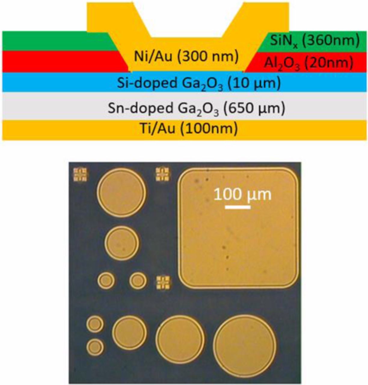
Figure 1. Field-plated Schottky rectifier schematic (top) and unit cell of fabricated devices (bottom).
Results and Discussion
In order to compare the dielectric stacks fairly, the device properties must be similar, thus C-V measurement was carried out to determine the intrinsic carrier concentration. Figure 2 shows the 1/C2-V characteristics used to extract the n-type donor concentration from the slope of the linear regime of this data. The carrier concentration was in the range of 3–5 × 1016 cm−3 in cases, indicating good uniformity.
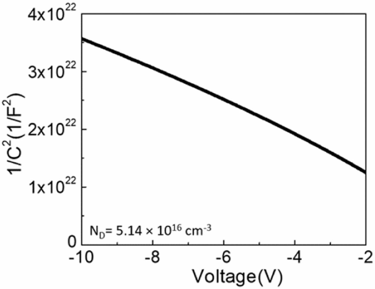
Figure 2. 1/C2 – V characteristics from a 200 μm diameter rectifier, giving a drift layer carrier concentration of 5.14 × 1016 cm−3.
Figure 3a shows the temperature dependence of forward J-V characteristics from 25–125°C for the 200 μm diameter diodes with dielectric stack Al2O3/SiNx. The zero-bias Schottky Barrier height and ideality factor (η) were extracted by fitting of the thermionic emission model to the linear region of the J-V curves. The average ideality factor, barrier height and On/Off ratio are presented at room temperature for each dielectric stack in Table I. The ideality factor and barrier height were fairly invariant across each sample and indicate the passivation plays little role in determining on-state characteristics. The Al2O3/SiNx stack produced the closest to ideal diodes, with an average ideality factor of 1.02 and a SBH of 1.14 eV. From the J-V vs T curves, a Richardson plot, Figure 3b, was generated and produced a Richardson constant of 48.06 A·cm−2·K−2, which aligns with previous reports.23,24,29,30 The on-state resistance values extracted from the linear regime of the J-V curves ranged from 3.8-5.0 × 10⁻³ Ω-cm2. These values are comparable to those found by Yang et al. (5.9 × 10⁻⁴ to 0.26 Ω-cm2).23
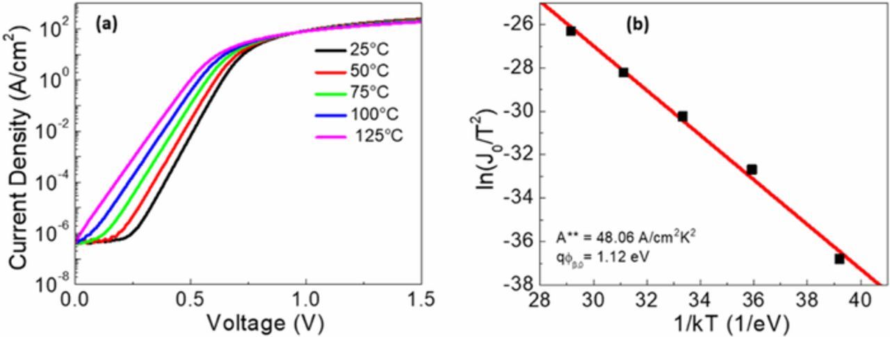
Figure 3. (a) Temperature dependence of forward current characteristics from 25 to 125°C and (b) Richardson plot with an extracted Richardson constant of 48.06 A/cm2K2.
Table I. Summary and comparison of dielectrics and their effect on forward characteristics for field-plated Schottky rectifiers.
| Dielectric Stack | SBH (eV) | Ideality Factor | On/Off Ratio (Current at +2V/−10V) |
|---|---|---|---|
| Al2O3/SiNx | 1.15 ± 0.03 | 1.02 ± 0.02 | 5.4 × 10¹⁰ |
| HfO2/SiNx | 1.14 ± 0.06 | 1.12 ± 0.06 | 2.1 × 10¹⁰ |
| SiO2/SiNx | 1.10 ± 0.07 | 1.15 ± 0.07 | 2.3 × 10¹⁰ |
In order to discuss the reverse characteristics, it is first important to identify the band alignment of the key oxides which are in immediate contact to the Ga2O3.31–33 These are shown in Figure 4. For a lateral MOSFET, 1 eV conduction and valence band offsets are generally accepted as the minimum offset required for a dielectric. However, with a vertical diode, the same rule does not apply necessarily as the dielectric is primarily present to lower the electrical field induced at the edges of the diode to prevent premature reverse breakdown. Based on this assessment, it would be expected that regardless of passivation on the Schottky surface, the reverse leakage current would be similar between dielectrics under low electric field conditions as the passivation has yet to play a significant role. However, Figure 5 shows this is not true. Al2O3 produces approximately an order of magnitude improvement in reverse leakage current. There are two primary reasons for Al2O3 achieving lower leakage current than SiO2. The SiO2 while having a larger conduction band offset than Al2O3 was deposited by PECVD and even with deposition parameters optimized to reduce the DC bias voltage on the sample to essentially zero, there may be some plasma induced damage. First, a charge on an insulator can induce a mirror charge on the opposing side of the insulator as such during the deposition as charged ions deposit, there must be an equilibrium of charge.34 At the start of deposition, the SiO2 layer is very thin and if the charge on the insulator is to exceed the breakdown capacitance of the thin SiO2, that will produce conducting defects in the insulator layer. Second, the slight ion bombardment will introduce interfacial defects between the semiconductor and the insulator.34–36 Post-PECVD annealing has been found to greatly improve the interfaces and insulators properties through reordering and removal of hydrogen content.35,36 Kim et al. performed a very similar comparison of ALD Al2O3 and PECVD SiO2 passivation, using SiGe as the substrate.37 Kim found the interfacial trap density to be more than an order of magnitude less for ALD Al2O3 than PECVD SiO2 and as a result the reverse leakage current was approximately 1 order of magnitude lower.
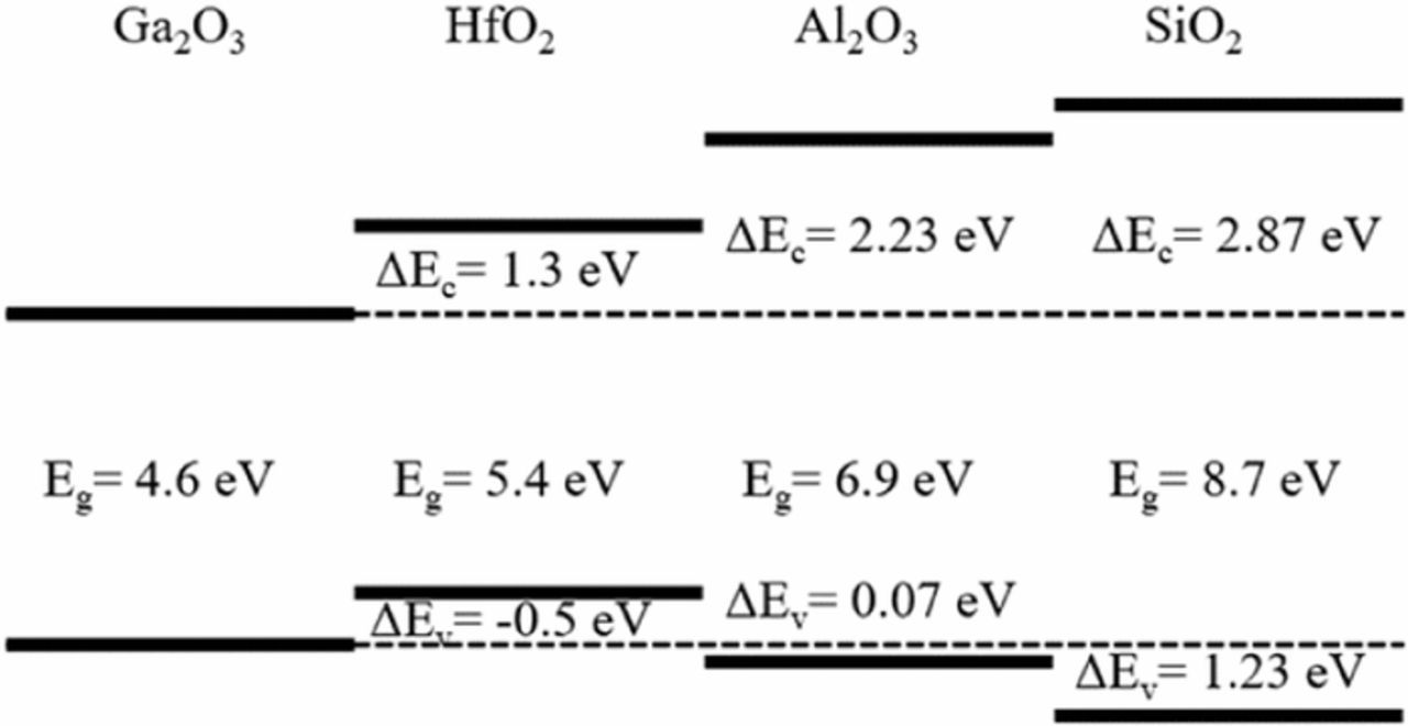
Figure 4. Band alignments of HfO2, Al2O3, and SiO2 to β-Ga2O3.
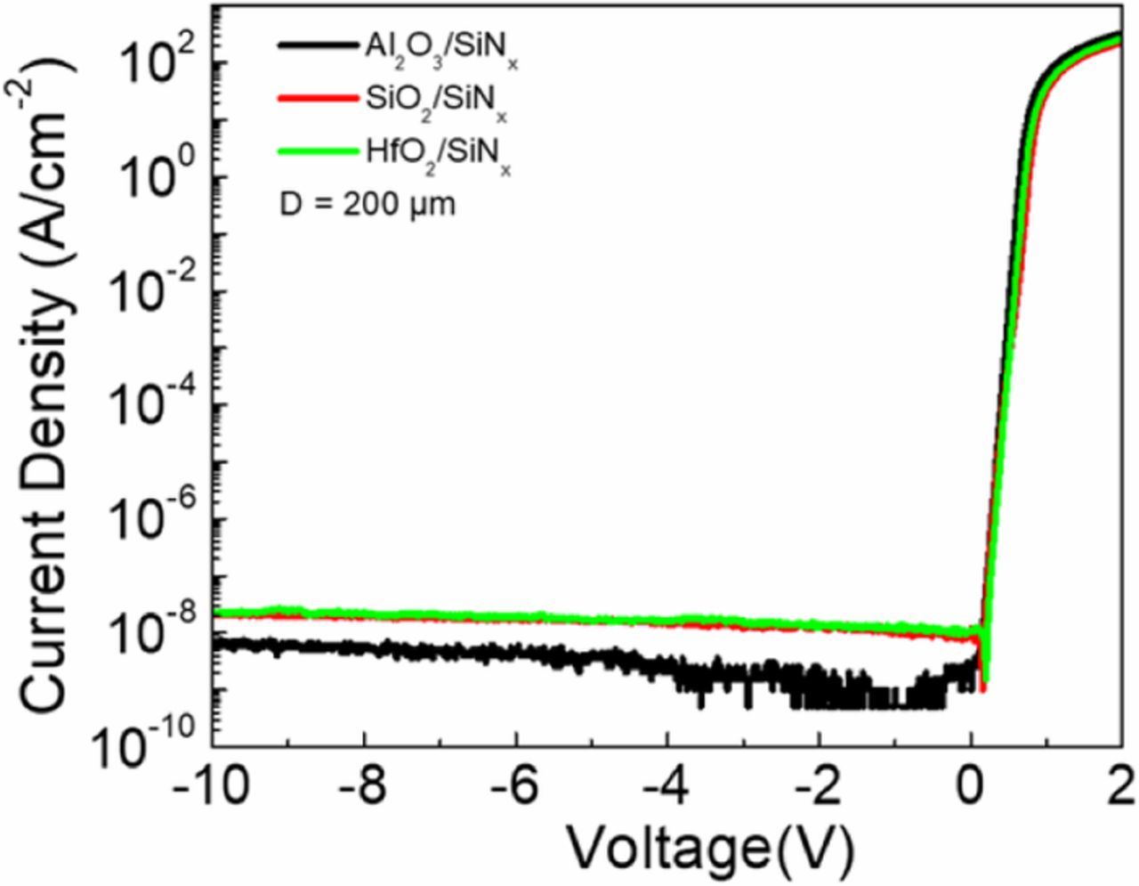
Figure 5. Low electric field J-V characteristics of 200 μm diameter diodes with varying dielectric stack.
Figure 6 presents a set of reverse breakdown measurements on diodes for each dielectric stack. Al2O3/SiNx field-plated diodes exhibited the highest breakdown of 730 V. Under high electric field, the properties of both Ga2O3 and the dielectric stack with the field plate become increasingly important. In our experiments, we noted that a defect would become visible after breakdown measurements on the field plate; indicating it is likely breakdown occurring at the edge termination region and not on the center rectifier region. At the edge of the Schottky contact, breakdown will occur when the electric field exceeds the critical breakdown strength of the Ga2O3 epi layer or dielectric stacks. The electric field in the dielectric layer can be approximated from Gauss's Law (Elow κ/Ehigh κ = κhigh κ/κlow κ). Gauss's law predicts that the breakdown will likely occur in the low k material due to the elevated electric field. This could be the main cause of rectifier terminated with SiO2/SiN undergoing failure. HfO2 has the lowest maximum breakdown strength as shown in Table II; therefore, the rectifier terminated with HfO2/SiN exhibits the lowest breakdown voltage. Likely, for both the HfO2 and SiO2 based field plates, failure is induced within these layers rather than within the nitride.
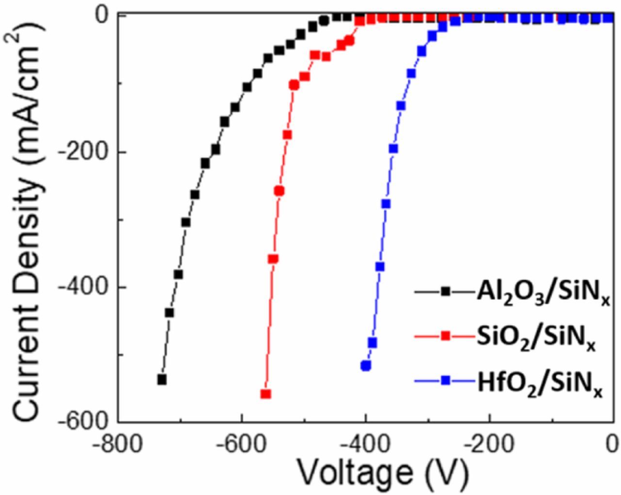
Figure 6. Reverse breakdown characteristics for field-plates with Al2O3/SiNx, HfO2/SiNx and SiO2/SiNx passivation.
Table II. Summary of key dielectric properties for simulated electric field.
| β-Ga2O3 | HfO2 | Al2O3 | SiO2 | SiNx | |
|---|---|---|---|---|---|
| Bandgap (eV) | 4.6 | 5.4 | 6.9 | 8.7 | 3.4 |
| ΔEc to Ga2O3 | - | 1.3 | 2.23 | 2.87 | - |
| ΔEv to Ga2O3 | - | −0.5 | 0.07 | 1.23 | - |
| Bulk Dielectric constant, ɛb | 10 | 25 | 9 | 3.9 | 7 |
| Thin Film Dielectric Constant, ɛtf | - | 15.538 | 739 | 3.940 | 641 |
| Eexp Dielectric (MV/cm) | - | - | 8.7 | - | 6.7 |
| Emax Theoretical (MV/cm) | 8 | >5 | 16 | >10 | 11 |
To determine which layer was failing in our highest performing field plate, Al2O3/SiNx, modeling of the estimated electric fields was performed via TCAD software FLOODS d. The model places the maximum peak at the edge of the field plate within the SiNx passivation, as shown in Figure 7. Key parameters for the simulation are presented in Table II. For the maximum breakdown of 730 V, the simulation predicts a peak value of 12.2 MV/cm and 7.1 MV/cm within the SiNx and Al2O3, respectively. To verify which layer of the field plate was failing, metal contacts were deposited across each individual dielectric to form a capacitor and test the vertical breakdown of each dielectric. The SiNx capacitor in this formation withstood a field of 6.7 MV/cm and the Al2O3 capacitor withstood a field of 8.7 MV/cm. This indicates that likely the SiNx layer was failing prematurely. This simulated result confirms our observation of a defect forming on the edge of the field plate during breakdown measurement and indicates the failure is likely within the nitride layer. The discrepancy of the simulated peak field and experimental can be attributed to the unknown taper angle of the wet etched field plate along with error in exact epi layer thickness that was achieved in chemical mechanical polishing of the test wafer.
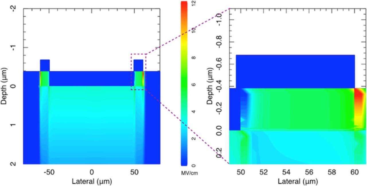
Figure 7. Simulated electric field distribution of the test device with an Al2O3/SiNx field plate at avalanche breakdown.
Conclusions
β-Ga2O3 Schottky diodes were fabricated with various dielectrics to delineate the effect of field plating parameters on the reverse breakdown. Al2O3/SiNx showed superior characteristics compared to HfO2/SiNx and SiO2/SiNx, due to the trade-off of bandgap and dielectric constant. Future efforts will focus on further tuning the field plate overlap length and dielectric thicknesses to maximize the reverse breakdown of the Schottky diode. These results discussed here provide a basis for comparing dielectrics based on their band alignments to Ga2O3 and demonstrates the need and promise for advanced electrical field mitigation techniques.
Acknowledgments
The project or effort depicted was partially sponsored by the Department of the Defense, Defense Threat Reduction Agency, HDTRA1-17-1-011, monitored by Jacob Calkins.
ORCID
Patrick H Carey IV 0000-0002-8826-3977
Fan Ren 0000-0001-9234-019X
Ribhu Sharma 0000-0001-5754-7873
Stephen J. Pearton 0000-0001-6498-1256