
Abstract
Via-Last metallization of High Aspect Ratio Through Silicon Via (HAR TSV) for 3D integration is challenging. Indeed, the formation of a uniform and conformal dielectric to insulate HAR TSVs in Via-Last process flow is difficult to achieve for any physical deposition process. In this study, we present the first reported HAR copper TSVs, insulated by highly conformal electrografted poly-4-vinylpyridine (P4VP) in Via-Last process-flow. As a demonstration, this allowed the metallization of HAR copper TSVs for die-to-die 3D integration of a 22 × 22 photodiode array tier onto a CMOS control electronics ASIC.

This is an open access article distributed under the terms of the Creative Commons Attribution 4.0 License (CC BY, http://creativecommons.org/licenses/by/4.0/), which permits unrestricted reuse of the work in any medium, provided the original work is properly cited.
The development of 3D Integrated Circuit (3D IC) is the complementary approach of microsystem miniaturization to maximize electrical device performances. 3D integration, where planar dies are stacked and connected to each other using Through Silicon Vias (TSV), allows better electrical performances, higher scale factor and advanced functionalities.1 TSVs are vertical interconnections insulated from the silicon substrate used to shorten the path between chips, reducing power consumption while increasing interconnection density and electrical performances.2 High aspect ratio TSV (HAR TSV) defines a TSV where its length is at least 8 times higher than its diameter.
Copper TSV fabrication is realized in 2 steps. First, a vertical hole is etched in the silicon substrate, traditionally by Deep Reactive Ion Etching (DRIE).3 Then the hole is metallized through the deposition of an insulator (to ensure electrical insulation of the interconnection), the deposition of a barrier layer (to prevent copper migration from the interconnection to the silicon substrate4) and the electroplating of the TSV copper filling (to ensure electrical conductivity of the interconnection). There are three approaches to integrate TSV metallization in the overall microsystem fabrication process flow: “Via-First” defines TSV metallization realized before the Front End of Line (FEOL) and the Back End of Line (BEOL) processes; “Via-Last” defines metallization realized after FEOL and BEOL processes. “Via-Middle”, which defines metallization realized between FEOL and BEOL.5 Copper TSV cannot be metallized in Via-First as the FEOL requires high temperature processes that cause copper diffusion into the silicon.6 For these reasons, doped polysilicon is used in Via-First7 or tungsten is used in Via-Middle.8 Unfortunately, these materials have lower electrical conductivity than copper. To be used in 3D IC, copper TSVs have to be metalized in Via-Middle or Via-Last. In either case, all processes for TSV metallization must be realized at temperature below ∼400°C to prevent any damage to the FEOL structures. In most cases, the TSV insulation layer is based on silicon dioxide (SiO2). As the growth of a thermal silicon dioxide is not compatible with the Via-Middle and the Via-Last approaches due to the temperature required, most of the SiO2 deposition technics use Chemical Vapor Deposition (CVD) based methods and are costly due to the growth conditions required to get a conformal insulator layer in deep structures.2 This point makes HAR copper TSV metallization challenging in the Via-Middle and Via-Last process flows in 3D integrated microsystem development.
Aveni (formerly known as Alchimer) has proposed a wet process flow to metalize HAR TSV, composed of a grafted polymer to electrically insulate the TSV, a chemical grafted nickel based layer for barrier diffusion layer and a final electrografted copper filling.9,10 The proposed alternative to SiO2 based dielectric uses an electrografted poly-4-vinylpyridine (P4VP) polymer to electrically insulate HAR TSV.11 The electrical properties of a P4VP electrografted film onto flat Si substrate, as measured by aveni and given in the Table I,12 show that P4VP dielectric film properties are comparable to SiO2. The main benefit of the electrografting process is the reduction in cost of ownership per wafer with respect to conventional dry approaches used to insulate HAR TSV with SiO2. Its capability to be implementable in any plating equipment, allowing savings compared to traditional dry process ones. Electrografted polymers smoothly follow surface topology13 and thus are insensitive to TSV scalloped walls, allowing Bosch process to be realized at a higher rate to reduce the overall TSV manufacturing costs. Moreover, electrografted P4VP is used as adhesion promoter for NiB electroless process. As the NiB layer is not only a good barrier to copper diffusion14 but also conductive enough for direct copper filling plating, there is no need of copper seed layer.14,15 Thus, TSV metallization can be achieved without the copper seed layer.
Table I. Electrical properties of P4VP electrografted film compared to SiO2.
| Parameters | P4VP | SiO2 |
|---|---|---|
| Dielectric Constant | 3.0 F/m | 3.9 - 4.2 F/m |
| Breakdown field | 28 MV/cm | 10 MV/cm |
| Leakage Current @ 0.25 MV/cm | 15 nA/cm² | 10 - 20 nA/cm² |
Electrografting creates covalent bonds between the silicon surface and the electrografted P4VP layer.9,13 It has been demonstrated that P4VP grafted on Silicon flat substrate passes a scribe tape test with 16 squares scribes (16/16 pass).9 The first evaluation of the electrografted P4VP capability to act as a copper diffusion barrier layer shows promising results, yet it has not been fully demonstrated.11 In the present case, the barrier diffusion property is realized through the electroless of the NiB layer on the electrografted polymer. It has been demonstrated that a thin NiB layer, chemically grafted to an electrografted P4VP insulator has equivalent barrier property than TiN.9,10 The full stack (polymer, NiB and Copper) passes a scribe tape test with 16 squares scribes (16/16 pass)9 on Si flat surface.
This technology has been demonstrated on bare silicon substrates etched with HAR TSV,9,12 which for example can be used for silicon interposers. To our knowledge, this method has not yet been demonstrated on CMOS devices after the BEOL processes. In this paper, we report on the successful use of electrografted P4VP to insulate HAR copper TSVs in a Via-Last approach on CMOS. As a demonstration, the metallization was performed for die-to-die 3D integration of a 22 × 22 photodiode array tier onto a CMOS control electronic ASIC.16
Experimental and Sample Preparation
HAR copper TSV metallization was realized in Via-Last process flow conditions on 23 × 23 mm p-type silicon coupons diced from a 150 mm CMOS wafer. On these coupons, 3 copies of the CMOS 22 × 22 photodiode array were present. The foundry encapsulating silicon nitride layer has been removed on the contact pads. A TSV is to be fabricated for each photodiode.
All further experiments were realized in a class 100 cleanroom laboratory. A ∼600 μm thick SiNx protective layer is deposited by Plasma Enhanced Chemical Vapor Deposition (PECVD) to protect the CMOS contact pads. HAR TSVs of 8 μm diameter (at mouth) for 50 μm depth were etched using DRIE Bosch process, then cleaned 10 minutes under O2 plasma to remove organic deposits from the DRIE process.17 Figure 1 presents a SEM image of a sample cross section of a TSV site after DRIE etching and prior to electrografting. The rugged texture is inherent to the DRIE etching process.
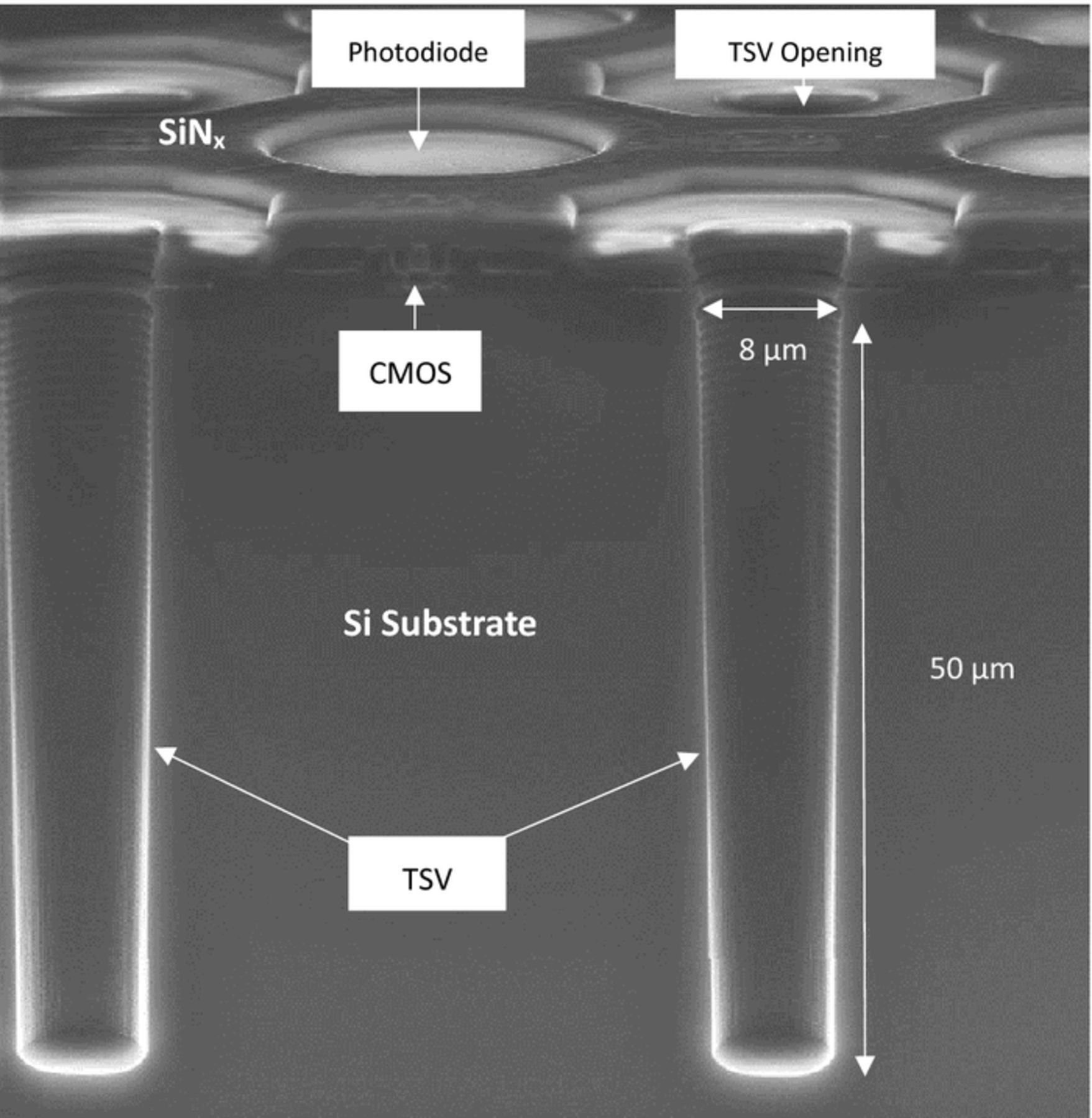
Figure 1. SEM image of a sample cross-section before TSV metallization.
The TSVs are holes of 8 microns of diameter at mouth and 50 microns depth. A key issue is to ensure that any process solutions penetrate properly such narrow structures. Therefore, before any wet processes (surface preparation and electrografting), the samples are rinsed using deionized water (DI water) and then dipped in a beaker containing DI water which is placed in a primary vacuum chamber for 5 minutes. As the pressure decreases in the chamber, trapped air is expelled from the TSVs and replaced by deionized water. The excess of water on top of the sample is removed with special care to not dry the wetted TSVs. This “pre-wet” method allows the chemicals to react with the TSV in its entirety. Between wet processes, samples are carefully rinsed with DI water.
Two different methods of surface preparation were tested. Method A is based on the so-called RCA clean commonly used in microelectronics.2 The first step consists of a surface cleaning prior to silicon dioxide removal. We used Standard Clean 1 (SC-1), a mixture of H2O2, NH4OH and H2O, to remove organic residues and particles from the silicon substrate. The second step used diluted HF to remove the native SiO2 on the TSV exposed silicon surface and to passivate that surface by the creation of Si-H hydrophobic terminations.18 The third step used a second SC-1 solution to remove organic residues and particles of the Si surface. This also creates a thin silicon dioxide layer19 (∼10 Å) along with a silanol functionalized (Si-OH bond) surface.18 The last step uses a Piranha solution (H2SO4:H2O2:H2O) to remove the remaining organic and metal contaminants.20 Piranha solutions are known to be particularly effective on organic residues.
In Method B, the first step is composed of an O2 plasma to remove organics prior to silicon dioxide removal. The second step used diluted HF to remove native SiO2 of the TSV exposed silicon surface and to passivate it with Si-H hydrophobic bonds. The sample is then rinsed and dried under N2. The third step uses an UV/Ozone cleaning to remove organics contaminants21 and to create a thin silicon oxide layer at the surface.22 Directly after the third step, the samples were dipped in water at room temperature for an extended period of time. The last step uses Piranha solution, to remove any remaining organic and metal contaminants.
The electrografting of P4VP is realized in a two electrodes electrochemical cell, using aveni's eG3D Isolation chemical solutions. We fabricated a sample holder, electrically connected to a Keithley 236 SMU. The sample, used as working electrode, is placed on a 25 × 25 mm recess realized in the center of the sample holder and is fixed using copper tape at its four edges allowing current to directly flow from the sample holder to the front side of the silicon sample. A fabricated O-ring is used to expose the desired area of the sample containing the HAR TSVs to the electrografting solution, while preventing the solution to reach the electrical contacts. A platinum ring is used as counter electrode. Reverse pulsed amperometry conditions are applied for 20 minutes at room temperature. After 20 minutes of electrografting process, a 130 to 160 nm thick layer of P4VP is grafted to the wall of the HAR TSVs (Figure 2). Other non-grafted P4VP chains23 are still present in the solution or adsorbed at the surface of the sample but were removed after rinsing of the sample. The samples are dried under N2 before anneal at 200°C under N2 to evaporate the remaining water contained in the polymer. Then a conductive NiB barrier layer is deposited by chemical grafting using aveni's cG3D Barrier chemical solutions.12 This electroless process creates strong chemical bonds between the electrografted polymer and the NiB layer. Bottom-up copper electrografting is realized using the NiB barrier as seed layer with aveni's eG3D fill chemical solutions.12 A final annealing is realized at 200°C under H2/N2.
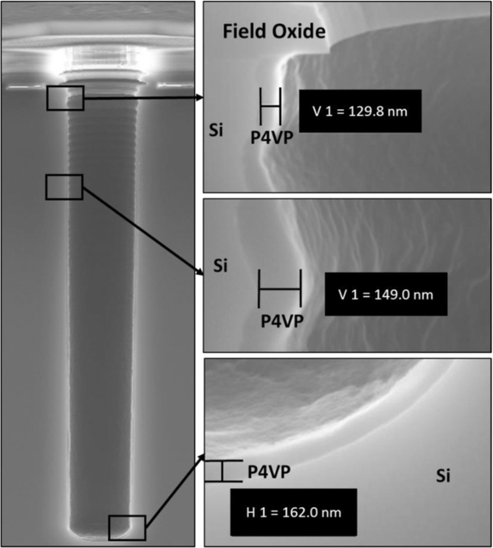
Figure 2. SEM image of a TSV cross section after P4VP electrografting. On the right, high magnification images at the top, middle and bottom the TSV showing the excellent P4VP coverage and uniformity.
Results and Discussion
The Figure 2 shows typical results obtained on a sample after P4VP electrografting with either of method A or B as surface preparation. The SEM images show that only the TSV walls are covered with the electrografted P4VP. Moreover, the electrografted P4VP follows closely the textured walls of the TSV. We also notice that, even with a field oxide overhang, the electrografted polymer covers perfectly all exposed silicon. This is a challenge for most physical deposition methods.
This excellent uniformity is due to electrografting growing mechanism. Electrografting methods are electro-initiated processes.13 In our case, because of the electrical contacts are realized on the edge of the silicon coupon, a faradaic current can only occur at the interface between the silicon surface of the HAR TSVs and the electrografting solution, other structures being protected by lower conductive materials (field oxide or SiN layer). Thus, P4VP can only be grafted at HAR TSVs silicon surface. The electrografting solution provided by aveni contains organic reactants in an aqueous acidic media: 4-nitrobezen diazonium (NBD) and monomers of 4-vinylpyridine (4VP). The electrografting mechanism of P4VP onto Si in aqueous media through reduction of diazonium salts is complex. However, a mechanism based on electrochemical initiation followed by a purely chemical polymerization has been proposed.12,24,25 In a first electro-initiated step, aryl radicals must be generated by the electrochemical reduction of NBD on the Si electrode. On p-type silicon, the Fermi level (EF) lay close to the silicon valence band (VB). All electronic energy levels below EF are occupied, those above likely to be empty. For the electrochemical reduction of NBD to occur, a voltage has to be applied to move the EF in more cathodic potential to reach the reduction potential of the NBD. In that case, electrons are able to transfer from the silicon electrode to the electrografting solution to reduce NBD at the interface: aryl radicals are generated by cleavage of the dinitrogen function according to the below equation, where “Ar” represents the aryl function:

During the cathodic pulse, EF is moved negative enough for aryl radicals to be generated. These aryl radicals can covalently bond to the silicon surface through an electron transfer and a thin polyphenylene (PNP) film grow through the reaction between aryl radicals as shown in the Scheme 1.26 Alternatively, other generated aryl radicals can initiate radical polymerization of 4VP monomers into P4VP:25 polymerization initiation through the reaction between NBD aryl radicals and 4VP monomer in the C=C double links, polymerization propagation and termination of polymerization through grafting to the PNP layer onto the substrate. Scheme 2 presents this mechanism.
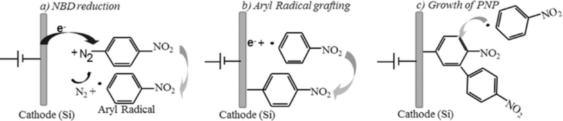
Scheme 1. Electrochemical reduction of NBD and PNP grafting onto Silicon substrate.
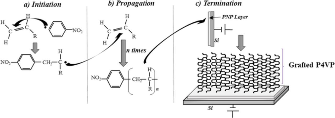
Scheme 2. 4VP radical polymerization initiated by NBD aryl radical. “R” represents the pyridine function of 4VP.
Experimentally, we observed that reverse pulse amperometry conditions applied on p-type Si-OH functionalized sample allowed the electrografting process of P4VP to grow faster and the grafted layer to be thicker. One of the hypotheses to explain this increase of kinetic and thickness could be the brutal inversion of the surface charge during the reverse pulse (anodic pulse): the polymer structure would stay opened by the creation of channels in the film, through desorption of physisorbed species, allowing reactive species to diffuse more easily from the electrografting solution to the silicon surface.27 This phenomenon could facilitate the generation of aryl radicals for the 4VP polymerization process to be maintained. Nevertheless, this hypothesis remain to be demonstrated. Figure 2 shows that the very top of the TSV wall, at the junction with the field oxide, is covered with ∼130 nm of P4VP, 20 microns deeper, the TSV is covered with ∼150 nm of P4VP, and the bottom of the TSV is covered with ∼160 nm of P4VP. With the use of electrografted P4VP we managed to obtain an excellent step coverage, up to 106% (ratio between thickness of the insulator on bottom and top of the TSV). The coverage properties of the electrografted P4VP is better than any other process considered so far for HAR TSV insulation in Via-Middle or Via-Last integration.
Figure 3 shows the result of the P4VP electrografting and metallization of HAR TSV after the Method A surface preparation. In some cases, the Method A surface preparation attacked the CMOS or contact pads through microscopic cracks or porosity of the added protective SiNx layer. A careful study of the problem lead us to link it to the use of the pre-wet vacuum chamber which enabled the surface preparation chemical solutions to reach the aluminum metal layers through cracks or porosity of the SiNx layer. The SC-1 and piranha chemical bath are known to be very aggressive on aluminum.20 Moreover, the generation of dioxygen bubbles during H2O2 decomposition contributes to deteriorate the protective SiNx layer when they are expelled, leading to extended damages. Even when using weakened (diluted) versions of the SC-1 and Piranha solutions, major damages were noticed.
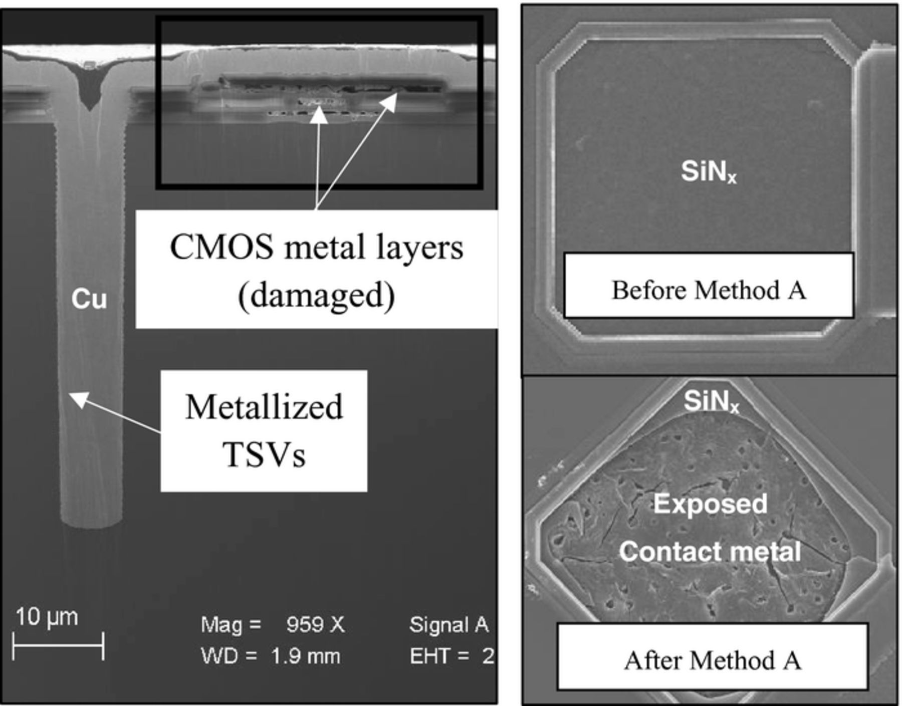
Figure 3. Left: SEM image of a sample cross section image after Method A surface preparation and metallization. Right: SEM image of contact the sample contact pad, before and after Method A surface preparation.
Figure 4 shows metallized TSV after the Method B surface preparation. In this figure, we clearly see that CMOS structures were not damaged by the surface preparation. The use of ozone and O2 plasmas process in replacement of aggressive chemical solutions, provides the adequate TSV side wall surface states for the P4VP electrografting without damaging CMOS metal structures. As a demonstration of the capability of HAR TSVs to be metallized in Via-Last using a P4VP electrografted process, Figure 5 shows a large part of the 22 × 22 matrix of TSVs in a CMOS technology metallized after the Method B surface preparation. After TSVs metallization, Cu overburden is also covering photodiode structures. This Cu will be stripped using an electrochemical solution.
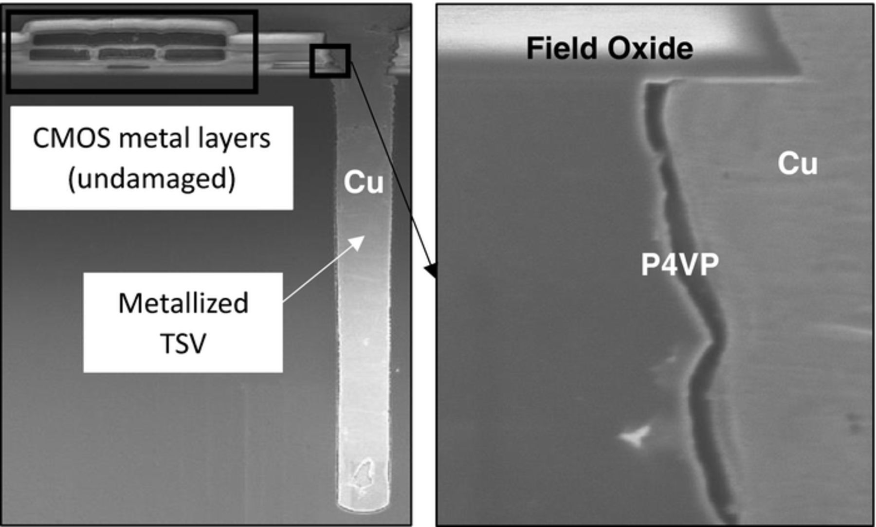
Figure 4. SEM cross sectional picture of HAR TSVs cleaned with the Method B surface preparation and metallized after BEOL process.
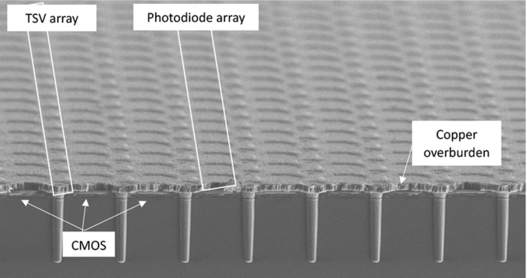
Figure 5. SEM picture of HAR TSVs (part of a 22 × 22 matrix) metallized in a Via-Last process flow using an electrografted P4VP layer as dielectric in a CMOS chip.
Summary
In this paper, we succeeded in electrografting P4VP to insulate HAR copper TSVs in a Via-Last process for die-to-die 3D integration of a 22 × 22 photodiode array tier onto a CMOS control electronics ASIC. We developed a gentle method for the surface preparation of the silicon that allowed the electrografting process to occur in HAR TSV without damaging the BEOL structures of the CMOS. The electrografted P4VP is only grafted on the Si side walls of the TSV, leaving any other surface free of dielectric. The polymer smoothly covers the scalloped side walls of the TSV with better coverage uniformity than most dielectrics considered in Via-Middle or Via-Last processes. We demonstrated the capability of electrografted P4VP to be an alternative to SiO2 based dielectric in HAR copper TSV metallization for Via-Last process flow.
Acknowledgments
This work was performed at Université de Sherbrooke supported by grants from the Natural Sciences and Engineering Research Council of Canada (NSERC), PRIMA, MITACS and PROMPT, with the contributions Teledyne DALSA Semiconductor and aveni.
