
Abstract
 films were grown on
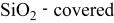 Si(111), and hydrogen‐terminated Si(111) substrates at a temperature of 500°C by ultrahigh vacuum ionized cluster beam deposition. The microstructures and growth behavior of these films have been investigated by transmission electron diffraction (TED) and high resolution transmission electron microscopy (HREM). The TED results show that the
 grown on the
 has the epitaxial relationship of
 and
 . The film on the H‐Si contains
 and amorphous
 layers at the interface, having the orientation relationship each other. For the
 and the Si substrate, the relationship is
 and
 . For the
 and the
 , the relationship is as follows:
 and
 ;
 and
 . The formation mechanism of the interfacial phases of
 ,
 , and
 are described. It is shown that the crystallinity of the
 film on the
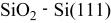 is better than that of
 on H‐Si(111). © 1999 The Electrochemical Society. All rights reserved.
Access this article
The computer you are using is not registered by an institution with a subscription to this article. Please choose one of the options below.
Purchase from
Purchase this article from our trusted document delivery partners.

Make a recommendation
To gain access to this content, please complete the Recommendation Form and we will follow up with your librarian or Institution on your behalf.
For corporate researchers we can also follow up directly with your R&D manager, or the information management contact at your company. Institutional subscribers have access to the current volume, plus a 10-year back file (where available).
