

Abstract
Atomic precision advanced manufacturing (APAM) offers creation of donor devices in an atomically thin layer doped beyond the solid solubility limit, enabling unique device physics. This presents an opportunity to use APAM as a pathfinding platform to investigate digital electronics at the atomic limit. Scaling to smaller transistors is increasingly difficult and expensive, necessitating the investigation of alternative fabrication paths that extend to the atomic scale. APAM donor devices can be created using a scanning tunneling microscope (STM). However, these devices are not currently compatible with industry standard fabrication processes. There exists a tradeoff between low thermal budget (LT) processes to limit dopant diffusion and high thermal budget (HT) processes to grow defect-free layers of epitaxial Si and gate oxide. To this end, we have developed an LT epitaxial Si cap and LT deposited Al2O3 gate oxide integrated with an atomically precise single-electron transistor (SET) that we use as an electrometer to characterize the quality of the gate stack. The surface-gated SET exhibits the expected Coulomb blockade behavior. However, the gate's leverage over the SET is limited by defects in the layers above the SET, including interfaces between the Si and oxide, and structural and chemical defects in the Si cap. We propose a more sophisticated gate stack and process flow that is predicted to improve performance in future atomic precision devices.
Export citation and abstract BibTeX RIS
1. Introduction
Exponential increases in tooling costs for successively smaller metal-oxide-semiconductor (MOS) transistor generations are becoming untenable as feature sizes shrink below a linear dimension of 10 nm (∼30 silicon atoms). To investigate potential device types and architectures before committing large capital investments for manufacturing, smaller scope research devices are necessary. This includes using tools that are inherently limited in scope to study proof-of-concept devices that demonstrate the physical viability of new device technologies beyond the next manufacturing node. One path to developing an understanding of device physics at the absolute limit of atoms themselves is atomic precision advanced manufacturing (APAM) [1]. In APAM, fabrication of nanoscale devices is achieved using a scanning tunneling microscope (STM) to pattern devices on the surface of Si. With this technology devices such as single-electron transistors (SETs) can be produced and used as sensitive electrometers to characterize the impact of different fabrication steps for process development. To date, many atomically precise (AP) devices such as tunnel junctions [2], SETs with a single quantum dot island [3–6], and a SET with a pair of independently controlled quantum dots [1] have been produced using delta-layer doping of P in Si above the solid solubility limit. However, such devices rely on intrinsic Si as a dielectric for in-plane gates rather than MOS surface gates. This limits the applicability of this pathway to the microelectronics industry, which is based on MOS field effect transistors.
The challenge of integrating MOS surface gates on top of AP devices derives from the need to maintain a low thermal budget [1]. There exists a tradeoff between low thermal budget (LT) processes to prevent dopant diffusion and high thermal budget (HT) processes to promote low material defect densities. The APAM process involves patterning a hydrogen mask [7–9] to design an AP device and incorporate a high, non-equilibrium concentration of dopants at the Si surface [10, 11]. Epitaxial Si encapsulation and subsequent process steps must occur at LT to prevent P diffusion and segregation both in the growth direction [12] and laterally. For traditional APAM in-plane gates, the dielectric is intrinsic Si. It is thus limited by the band gap of Si with no offset between the device and the gate. For example, a transistor with an in-plane gate 38 nm from the channel leaks at 0.5 V at 80 mK [13], while a MOS gate with an oxide dielectric barrier of 20 nm or thinner would be expected to sustain 10 V with minimal leakage [14]. Minimizing leakage and increasing transconductance are critical for the low-power operation of digital logic devices, further motivating a move from in-plane to surface gates. Finally, operation at room temperature or higher is critical to effectively investigate the path forward for improving the performance of complementary metal-oxide-semiconductor (CMOS) devices. To date APAM devices have only operated at cryogenic temperatures (e.g. 4 K), 'freezing out' lightly doped Si and rendering it an effective gate dielectric. For room temperature operation this will not be the case, necessitating an insulator between the gate and the APAM channel.
Standard thermal SiO2 provides the simplest path to a clean dielectric but it is not thermally compatible with APAM. The required processing temperature will cause aggressive diffusion of the dopants. A MOS-gated SET has been created once through a unique in situ Si and O codeposition at room temperature [15] to grow SiO2 after Si encapsulation of an APAM SET also including an in-plane gate. This additional surface gate was demonstrated to improve the performance of the in-plane gate [13]. An alternative is to use an ex situ deposited oxide, which allows investigation of high-k dielectrics that decrease tunneling leakage and maintain high capacitance for effective gating with thinner layers. Deposited high-k dielectrics have already been implemented in industrial fabs, underscoring their compatibility with CMOS and the feasibility of integrating APAM devices with CMOS process flows.
In this paper we discuss the performance of an APAM SET integrated with a high-k gate oxide, Al2O3, deposited by atomic layer deposition (ALD). We use this SET as an in-channel electrometer to evaluate the quality of the gate stack and to understand device performance. We characterize this gate stack with cross-sectional scanning transmission electron microscopy (STEM) and secondary ion mass spectrometry (SIMS) to identify process defects and discuss the impact of these defects on SET performance. Finally, we propose a gate material stack that promises to overcome these process defects to improve future device performance.
2. Experimental procedure
Front-end-of-line (FEOL) fabrication, STM device patterning, and back-end-of-line (BEOL) processing were executed using previously described methods [1, 16]. FEOL produced chips with As implants for contacts to the APAM devices and alignment marks that are discernable in the STM. Next, oxide removal, device patterning via STM hydrogen depassivation lithography (HDL), PH3 dosing, and Si molecular beam epitaxy (using an MBE Komponenten Si sublimation (SUSI) source) occurred in ultra-high vacuum (UHV) chambers to produce an APAM SET encapsulated with 30 nm of Si. An STM image of this SET is shown in figure 1(a), where the bright regions are the patterned areas that have had the H removed to allow the incorporation of P that comprises the nanostructures. BEOL consisted of etching vias and depositing Al to contact the As implants that contact the APAM devices. A surface gate was added to the APAM SET by first depositing the gate dielectric, annealing in forming gas in a rapid thermal annealer, and finally depositing an Al gate electrode. During process development we compared SiO2 and Al2O3 films deposited using plasma-enhanced chemical vapor deposition and ALD, respectively (see supplementary material (available at stacks.iop.org/JPhysMaterials/03/035002/mmedia)). The gate dielectric of this SET is 30 nm of Al2O3 deposited by ALD at 200 °C with trimethyl aluminum and water precursors. A cross-sectional schematic of a completed device is shown in figure 1(b). It is important to note that unlike a traditional field effect transistor, the epitaxial Si immediately beneath the gate oxide is effectively part of the gate stack. The channel is the P-doped APAM SET. Finally, electrical testing of the fabricated SET was conducted at 4 K.
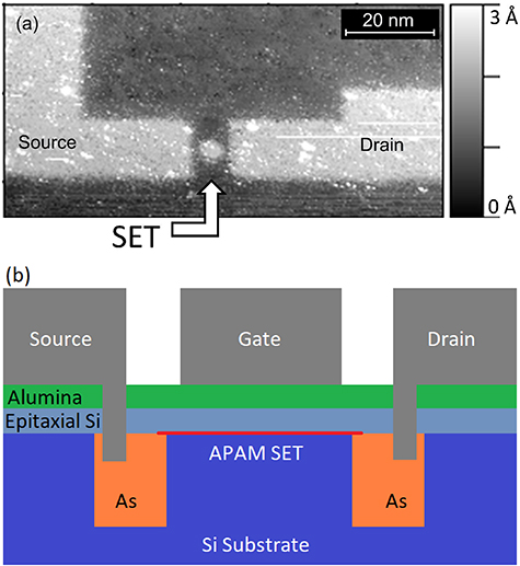
Figure 1. (a) STM image of SET after H depassivation lithography before creating the MOS gate stack. (b) Schematic cross section of a completed MOS gate stack consisting of Al2O3 for the oxide and Al for the electrode on top of an APAM device and As implants to contact the APAM SET.
Download figure:
Standard image High-resolution image3. Results and discussion
We infer that the SET survived the BEOL processing and gate deposition by the presence of the characteristic diamond structure in the source-drain current, as a function of source-drain and gate bias, that typifies Coulomb blockade [17] (figure 2(a)). The presence of Coulomb diamonds is evidence that the P donors remained in place with minimal diffusion. If the dopants diffuse a few nanometers in-plane, they will fill the tunnel barriers between the island and the leads (figure 1(a)) and the device will behave as a nanowire. If the dopants diffuse significantly either in-plane or out-of-plane, the carrier concentration will become too low to conduct at 4 K and the device will behave as an open circuit. Here we evaluate the performance of the top-gated device in terms of the leverage of the gate on the SET, which we define in terms of the ratio of the charging energy of the SET (diamond amplitude) to the voltage applied to the gate needed to change the charge state of the SET by one electron (diamond period). For this top-gated device the island is a single 5–7 nm radius feature (figure 1(a)), with uncertainty as to the final atomic and effective electronic device dimensions after fabrication. We observe a charging energy of approximately 6 meV for approximately 0.3 V applied on the gate between charging events, indicating that the gate leverages the SET by ∼20 meV V−1. Overall, our data compare well both to a previous effort with a leverage of ∼33 meV V−1 for an in-plane gated APAM SET that also included an unconventional top gate [13], and our own data for an in-plane gated APAM SET produced without a top gate (see supplementary material). Assuming ideal dielectric permitivities for both our 30 nm Si cap and 30 nm Al2O3 dielectric and an island radius of 6 nm, we calculate an island-gate capacitance of approximately 1 aF and an island self-capacitance of approximately 5 aF. This yields a capacitance-defined leverage of 0.2, compared to 0.36 for an in-plane gate in prior work [13].

Figure 2. (a) Absolute source-drain current as a function of gate bias and source-drain bias for an APAM SET with a top gate exhibiting the characteristic diamond structure of Coulomb blockade, leading to ∼6 meV charging energy (diamond amplitude) for a change of ∼0.3 V on the gate (diamond period). (b) Source-drain current for the SET for forward and reverse sweeps of the gate bias at a source-drain bias of 1 mV.
Download figure:
Standard image High-resolution imageThe results above demonstrate that a low-temperature ALD oxide is a viable path forward for producing an APAM device with a MOS surface gate. The ability to apply a higher gate bias with a MOS surface gate (see supplementary material) is valuable for quantum information applications, where a large gate bias is required to control the number of electrons on the island. For digital logic applications, high transconductance translates to low operating voltages and power consumption. However, our surface-gated SET has not achieved superior performance; it has similar leverage to another SET with an APAM in-plane gate. Numerical modeling suggests qualitatively that we should examine the quality of the Al2O3 gate oxide and interfaces between materials to understand how to optimize the gate stack (see supplementary material). This is reinforced by the data in Figure 2(b), showing that the SET source-drain current (at a source-drain bias of 1 mV) suffers from hysteresis on subsequent gate bias sweeps in opposite directions over the range of −4 V to 3 V. This hysteresis suggests that there exist trap states in the epitaxial Si, the Al2O3, the Si/Al2O3 interface [18], and/or the Al/Al2O3 interface. These traps could be caused by structural and chemical defects, which would be consistent with LT Si homoepitaxy [19] (though this can be mitigated with extremely slow Si growth [20]) and LT ALD of Al2O3 on Si [21], respectively.
Material characterization reveals defects and impurities that are consistent with the observed gate hysteresis. Impurities in the silicon cap could create trap states that cause hysteresis or generate carriers that screen the field applied by the gate, noting that the epitaxial Si is effectively part of the gate stack above the P-doped APAM channel. Figure 3 shows a SIMS depth profile of an epitaxial cap, grown under similar conditions to that of the SET, with incorporated O and Al. These concentrations are 7 × 10¹⁹ atoms cm−3 O and 4 × 10¹⁸ atoms cm−3 Al in the cap with 1 × 10¹⁷ atoms cm−3 O and 1 × 10¹⁵ atoms cm−3 Al (roughly the detection limit for Al in Si) in the substrate. Similar results have been reported previously for this LT Si epitaxy process on another similar sample, though that sample exhibited a higher concentration of chemical defects (C, O, and N) at the cap/substrate interface [22]. The C, N, and O concentrations are influenced by the Si growth temperatures [22] and are limited by the chamber background pressure during growth, which is approximately 1 × 10⁻⁸ Torr. We suspect that the Al impurities come from the SUSI source, as similarly prepared films capped with a different silicon source in the same chamber have not contained Al. While O is typically a deep level state, it can exist at a shallow energy level on its own [23], or in a complex with N [24], and become electronically active. Al is a shallow acceptor and impacts gate performance.

Figure 3. SIMS depth profile of epitaxial Si grown under similar conditions to that of the APAM SET and APAM nanowire.
Download figure:
Standard image High-resolution imageSTEM reveals further material defects in the gate stack. For an APAM nanowire with ALD Al2O3 on top of an epitaxial Si cap deposited similarly to the SET, STEM reveals an uncontrolled SiO2 layer approximately 4 nm thick at the interface between the Al2O3 and the Si, which is visible as the darker region between the lighter Al2O3 and lighter crystalline Si (figure 4). We expect a high interfacial trap density due to the poor interface between Al2O3 and Si in our samples [25]. The presence of this SiO2 layer effectively decreases the average dielectric constant of the gate stack and, in turn, the gate's capacitance over the SET. Additionally, figure 4 shows that there are structural defects in the epitaxial Si near the oxide, which are visible as darker regions in the high angle annular dark field (HAADF) image partially obscuring the bright, periodic columns of Si atoms. These defects might indicate partial amorphization of the cap or the formation of (111) twin domains near the Si/oxide interface. Amorphous Si or twin boundaries could introduce electronically active states and contribute to the observed gate hysteresis (figure 2(b)).

Figure 4. STEM HAADF image of cross sections of a nanowire with ALD Al2O3 atop the epitaxial Si, prepared under similar conditions to the SET. The bright spots in the oxide are due to damage from focused ion beam used to prepare the STEM sample. Note: the nanowire is not discernable in this cross section and might not be contained within it.
Download figure:
Standard image High-resolution image
In general, the interface with the highest density of interface states should have the largest impact on device performance in terms of gate leverage. Qualitatively, in a simple linear model, the Si/Al2O3 interface is likely the most important. Since the gate leverage over the SET depends on both the island self-capacitance and the gate-island capacitance, the leverage will be decreased by electronically active defects at all of the interfaces in the gate stack. The island self-capacitance will only be influenced by the defects in the island, that is, over a small region of the Si/P-doped Si interface. The contribution of defects elsewhere in that plane to the self-capacitance is negligible. The decrease in leverage will largely be driven by the decreased gate-island capacitance. Within a particular range of bias conditions, the gate-island capacitance will be reduced relative to what it would be in the absence of interface traps by an amount determined by the density of trap states, within those bias conditions, at all interfaces between the gate and the island. The gate-island capacitance is effectively reduced by the leverage that the gate has over the traps between the gate and island, so reducing the density of trap states is critical to realizing ideal performance. However, the density of trap states in a given device is dependent on the processing conditions and the quality of the interfaces, which is a subject of further study for the material stack and processing workflow at hand. Finally, the Al/Al2O3 interface is less important than the Si/Al2O3 interface. Traps at these interfaces must be compensated by either the channel or the gate. The further traps are from either interface, the stronger the field and the effect on leverage will be. The Si/Al2O3 interface is far from either the channel or the gate and will have a larger effect on leverage, than the Al/Al2O3 interface. Moreover, as a good metal, Al will be more effective than Si in screening the charged trap states, reducing the field that they produce at the island.
Many of the materials defects examined above can be reduced, or their effects mitigated, by adding to the complexity of the relatively simple material stack presented here. Our observed SiO2 interface layer is consistent with, though thicker than, previous reports [14, 21, 26]. This could be mitigated by intentionally depositing a thinner SiO2 [27] or Si3N4 [28] layer to act as a diffusion barrier before Al2O3 deposition. Additionally, the electrode/oxide interface can be improved by depositing barrier layers like TiN or TaN to prevent the Al from reducing the oxide when in direct contact [29, 30]. An additional TiN or TaN layer on top of Al would protect the Al from formation of a native oxide and improve electrical contact to the gate itself. Furthermore, deposited HfO2 could replace Al2O3 as it has a higher dielectric constant, allowing a smaller 'effective oxide thickness' [25].
The performance of the SET can be further improved through optimizing the geometry of the gate stack and the STM-patterned part of device. Assuming the island self-capacitance is only dependent on the in-plane geometry, gate leverage can be increased by making the layers of the gate stack thinner. Thinner layers move the gate closer to the SET (device channel), thus increasing the capacitance and therefore the capacitance-defined leverage of the gate over the SET. The epitaxial Si cap could be thinned to approximately 5 nm before surface scattering and the effects of limited out-of-plane P diffusion on device resistivity become significant [31]. An ideal oxide layer, assuming no pinhole defects, could also be thinned to a few nanometers before leakage becomes a concern [25]. Taking the more conservative thickness of 10 nm for both the Si cap and Al2O3, would make the gate stack a third of the thickness of the current device and triple the gate capacitance and leverage, assuming a simplistic model of the electrostatics. Finally, the geometry of the SET island and leads, including their sizes, shapes, and spacing could be further optimized to increase gate leverage, confinement energy, number of electrons on the island, and period of the Coulomb diamonds [5, 6, 32].
4. Conclusions
We have developed a simple, low thermal budget high-k/metal gate stack, using ALD Al2O3 as the high-k dielectric, that is compatible with APAM devices to enable investigation of physical principles for future digital device generations. We have evaluated the performance of this surface-gate stack for an APAM SET and observed the characteristic Coulomb blockade with a gate leverage of 20 meV V−1, indicating that the SET survived the BEOL processing to deposit the gate stack. However, this gate is hysteretic, which is the consequence of process defects including low-quality interfaces and structural defects in the Si cap as observed by STEM, in addition to O and Al that were unintentionally incorporated into the Si cap as observed by SIMS. To improve the performance of the surface gate, we propose a new gate stack with a diffusion barrier such as TiN or TaN between the Al and high-k dielectric layers, a controlled deposition of SiO2 or Si3N4 to act as a diffusion barrier for the interface between the Si cap and high-k dielectric, investigation of alternative dielectrics, and improvement of the Si epitaxy. A more advanced material stack, combined with additional optimization of the APAM process, should reduce the hysteresis, and improve the leverage of the gate. By reducing the role of impurities and defects, a more advanced material stack may also improve the ability of simple capacitive models to capture the measured behavior. Optimizing the Si/Al2O3 interface is likely to have the largest impact on improving gate leverage. Additionally, thinning the epitaxial Si and dielectric to 10 nm each should triple the leverage of the gate over the SET.
The surface gate stack demonstrated here, along with our proposed improvements, advance APAM as a technology for investigating physical principles that will aid the development of next-generation transistor nodes and Si:P-based quantum devices. Both applications require high-performance gates. Digital logic devices require high transconductance to switch devices with low power consumption. This requires gates that are as close to the device channel as possible with minimal leakage, both of which are enabled by high-k gate dielectrics. Digital logic devices must also be operated at room temperature or higher to be practical. APAM in-plane gates are prone to leakage, which is exacerbated at room temperature, suggesting that surface gates are a necessary advance for exploring this application space. To access a wide range of charge configurations for donor-based quantum devices, the large energy scales for donors drives the need for higher transconductance devices and larger voltages of operation. Leakage through the intrinsic Si dielectric imposes a lower bound on the separation between the gate and device, effectively upper bounding the achievable capacitance. In contrast, a surface gate with a high-k dielectric can be placed much closer to the channel and can be driven to higher bias without concerns about leakage.
Acknowledgments
The Far-reaching Applications, Implications and Realization of Digital Electronics at the Atomic Limit (FAIR DEAL) project is supported by the Laboratory Directed Research and Development program at Sandia National Laboratories, and was performed, in part, at the Center for Integrated Nanotechnologies, a US DOE, Office of Basic Energy Sciences user facility. Sandia National Laboratories is a multimission laboratory managed and operated by National Technology and Engineering Solutions of Sandia, LLC, a wholly owned subsidiary of Honeywell International, Inc., for the US Department of Energy's National Nuclear Security Administration under contract DE-NA-0003525. This paper describes objective technical results and analysis. Any subjective views or opinions that might be expressed in the paper do not necessarily represent the views of the U.S. Department of Energy or the United States Government.
Supplementary Material
Supplementary material for this article is available online