

Abstract
Epitaxial graphene on SiC is the most promising substrate for the next generation 2D electronics, due to the possibility to fabricate 2D heterostructures directly on it, opening the door to the use of all technological processes developed for silicon electronics. To obtain a suitable material for large scale applications, it is essential to achieve perfect control of size, quality, growth rate and thickness. Here we show that this control on epitaxial graphene can be achieved by exploiting the face-to-face annealing of SiC in ultra-high vacuum. With this method, Si atoms trapped in the narrow space between two SiC wafers at high temperatures contribute to the reduction of the Si sublimation rate, allowing to achieve smooth and virtually defect free single graphene layers. We analyse the products obtained on both on-axis and off-axis 4H-SiC substrates in a wide range of temperatures (1300 °C–1500 °C), determining the growth law with the help of x-ray photoelectron spectroscopy (XPS). Our epitaxial graphene on SiC has terrace widths up to 10 μm (on-axis) and 500 nm (off-axis) as demonstrated by atomic force microscopy and scanning tunnelling microscopy, while XPS and Raman spectroscopy confirm high purity and crystalline quality.
Export citation and abstract BibTeX RIS
1. Introduction
Two-dimensional graphene was first isolated in 2003 using Scotch tape to mechanically exfoliate graphene monolayers from graphite [1, 2]. This peeling technique could generate graphene flakes of up to 100 μm for laboratory research [3]. Mechanical and other chemical exfoliation techniques proposed after graphene's isolation [4] are not suitable to large scale applications in electronics, as it is not possible to achieve a perfect control of the quality of graphene and of the number of layers [5–7]. Transfer of graphene to the required substrate is also costly, time consuming and can cause defects and contamination at the graphene/substrate interface [8–11].
Epitaxial graphene on SiC obtained by Si sublimation in ultra-high vacuum (UHV) for the first time in 2004 [12], remains a promising route towards graphene-based electronics as it relies on the well-established semiconductor technology production chain [13]. Other techniques to obtain epitaxial graphene have been demonstrated, like direct synthesis of planar graphene on Ni substrate by thermal chemical vapor deposition (CVD) [14]. The morphology of the metal substrates determines the quality and structure of graphene, and many techniques are used to treat the surface for the production of high-quality uniform graphene layers such as annealing under CH4 or plasma treatment [15, 16]. However, the complicated process of transferring graphene layer to another substrate gives origin to defects and makes these methods not suitable for large scale electronics applications. Sublimation of SiC at high temperature is the most justified, scalable, and simple way of producing large scale, uniform, high quality graphene on a semiconducting substrate [17–19]. Graphitization of SiC by decomposition at high temperature in ultrahigh vacuum was first reported in 1962 while studying the transition of the surface structure of SiC at different temperatures but the number of graphene layers was unknown [20]. De Heer was the first to grow epitaxial graphene on 6H-SiC by Si sublimation in UHV [21, 22].
The growth of epitaxial graphene on semi-insulating SiC opens the way to a new generation of electronics, however it is imperative to achieve a perfect control of defects, surface structure and number of graphene layers [23, 24] to obtain the qualities required by the electronic industry. Several studies report about the growth optimization of epitaxial graphene obtained by thermal decomposition on different polytypes of SiC (6H, 4H and 3C) in ambient pressure or under UHV conditions [17, 25–30]. Growth of epitaxial graphene at atmospheric pressure requires high temperatures (1500–1700 °C) [31] which causes a high level of SiC step bunching, while it can be obtained in UHV at lower temperature with a reduced step bunching [17, 32]. During thermal decomposition Si atoms sublimate and the remaining carbon atoms diffuse and reorganize on the surface, forming the graphene honeycomb lattice [33–37]. The different polytypes of SiC have different surface free energies which influence the graphene growth mechanism [38, 39]. On 4H-SiC the sublimation of Si from the surface of SiC under UHV starts at temperatures above 1200 °C and the optimum growth condition results in epitaxial graphene with terraces of up to 200 nm width [40]. The slower the sublimation rate of Si, the higher the quality of epitaxial graphene as the carbon atoms have enough time to rearrange and form crystal domains [41, 42]. So far sublimation rate of Si is reported to be controlled by techniques such as Confinement Controlled Sublimation (CCS), supplying Si vapour, flowing inert gas and polymer assisted sublimation [42, 43]. These techniques are used to induce a counter pressure at the surface to minimize Si sublimation and create nearly equilibrium conditions for evaporating Si [27]. Although the CCS of Si for growth of epitaxial graphene is not a new technique, the sublimation of Si was obtained in previous works using an induction furnace under ambient or low pressure and using a graphite box to control the sublimation rate. The reported epitaxial graphene grown on 6H-SiC using CCS of Si has terrace size of up to 2 μm [42, 44].
In the present research, the face-to-face (FTF) technique is used to grow high quality epitaxial graphene with significantly large epitaxial graphene steps (∼10 μm (on-axis) and ∼500 nm (off-axis)) on 4H-SiC. A similar technique was previously used to grow monolayer epitaxial graphene on 6H-SiC under high vacuum (10–6 Torr) in a limited range of temperatures with terrace size of up to 1 μm and pits on the surface [45]. In our experiment, we extended the method of ref [45] to UHV (10–10 mbar), which allowed shorter growth times and lower temperatures improving the quality of graphene and controlling precisely the number of layers. We also used both on-axis and off-axis 4H-SiC and performed the experiment in an extended range of temperatures and for different durations, providing a full account of the graphene quality and thickness from 1260 °C to 1500 °C and for times variable between 5 min and 20 min, determining the growth law of graphene on both on-axis and off-axis 4H-SiC.
The FTF technique provides a very simple solution to slow down the evaporation of Si and effectively control the growth rate and structure of graphene with the advantage of growing two samples at the same time. The growth parameters on both on-axis and off-axis SiC are optimized based on the desired number of graphene layers and terrace size. We develop a kinetic model to explain the time evolution of the graphene layer by comparing the intensity of the C1s core level XPS spectra in SiC and graphene as a function of time and annealing temperature. Our model supports the layer-by-layer growth of epitaxial graphene and allows us to calculate the activation energy of the process.
1.1. Experimental method
1.1.1. Epitaxial graphene synthesis
Initially, samples were cleaned under sonication in acetone, ethanol, and deionized water for 20 min each and dried in the air before mounting on the sample holder. Two SiC substrates were sandwiched with the Si faces facing each other, separated by two pieces of tantalum foil 25 μm thick (99.9% purity, Goodfellow). Figure 1(a) illustrates the sandwich of SiC samples mounted on the direct current sample holder (Scienta Omicron GmbH) under a magnifier. Samples were introduced into an ultrahigh vacuum system (Scienta Omicron GmbH) and degassed overnight at 650 °C to remove contaminants. Epitaxial graphene was grown on both on-axis and 4˚ off-axis n-type 4H-SiC(0001) wafers (CREE, Double sided polish Si face CMP epi ready) using thermal decomposition (direct current heating) at ≥1260 °C for different period of times at a base pressure of ∼1 × 10⁻¹⁰ mbar (figure 1(b)). An optical pyrometer with temperature uncertainty of ±10 °C was used to monitor the temperature of the substrates (emissivity = 0.95). Several growths were performed to follow the evolution of the epitaxial graphene on both substrates. Figure 1(c) illustrates the mechanism of growth in the FTF technique and how the Si counter pressure on the SiC surface from the adjacent sample helps to control the growth rate and improves the structure of epitaxial graphene steps. To prove the effectiveness of FTF growth technique, epitaxial graphene was grown on both on-axis and 4˚ off-axis SiC by standard method of thermal decomposition as well. In this method, single SiC substrates were annealed at ≥1280 °C for different period of times at a base pressure of ∼1 × 10⁻¹⁰ mbar.
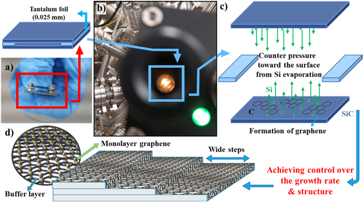
Figure 1. Our demonstrated concept of FTF growth technique enables control over the growth rate and structure of epitaxial graphene on SiC. (a) The sandwich of two SiC samples mounted on the sample holder for epitaxial graphene growth using the FTF technique. (b) The sample in (a) as seen through the optical pyrometer while annealing at high temperature in an UHV system. (c) The schematic model of growth mechanism. (d) The model of monolayer epitaxial graphene covering the SiC steps.
Download figure:
Standard image High-resolution imageAfter removing the samples from vacuum and separating the two wafers, atomic resolution imaging of the surface was obtained by mounting one of the two samples in a scanning tunnelling microscopy (STM) sample holder and re-introducing it quickly into the vacuum. The same sample was then analysed ex situ by atomic force microscopy (AFM) to visualize the large-scale surface structure and by XPS the number of graphene layers was calculated. The existence of epitaxial graphene and the number of graphene layers were further confirmed using Raman spectroscopy. Different phases of partially FTF grown epitaxial graphene were shown by Kelvin Probe Force Microscopy (KPFM). Figure 1(d) shows the schematic diagram of monolayer epitaxial graphene on SiC with a buffer layer. The morphology of the samples grown by standard technique was analysed in situ by STM after growth (figure S2).
1.1.2. Material characterization
The morphology of epitaxial graphene was studied using AFM and STM. A Dimension Icon PT (Bruker) was used to acquire the AFM images at room temperature using a ScanAsyst in Air probe under PeakForce tapping mode. Room temperature STM was conducted in a Scienta Omicron GmbH ultrahigh vacuum system with a base pressure of ∼ 1 × 10–11 mbar using an electrochemically etched W tip. A Variable Temperature (VT-AFM/XA) scanning tunnelling microscope was used to obtain the STM images at room temperature. Samples were degassed at 300 °C for two hours by electron bombardment in ultra-high vacuum before STM. AFM and STM images were analysed using Gwyddion software (http://gwyddion.net/). Kelvin probe force microscopy (KPFM) measurements were acquired with an Asylum Cypher-S atomic force microscope (Oxford Instruments) using Pt coated Si cantilevers with a spring constant of 7 Nm 1 (SPARK70Pt, NuNano). The KPFM measurement is a two-pass technique where, on the second pass, the tip is raised 3 nm above the surface and retraces the surface topography with AC and DC biases applied to the tip. For the data reported a 500 mV AC voltage (frequency matched to the cantilever drive frequency), and a 3 V DC voltage was applied to the tip. The chemical composition of epitaxial graphene was obtained ex situ by x-ray photoelectron spectroscopy (XPS) in a Kratos Axis Supra system. XPS measurements were acquired with monochromatic Al Kɑ radiation (1486.7 eV, 225W), and high-resolution core level spectra were collected at a pass energy of 20 eV whereas the survey spectra were collected at 160 eV pass energy. The XPS data were analysed using CasaXPS software (http://www.casaxps.com/) [46] and the binding energy of the components were calibrated based on Si 2p3/2 core level in SiC at 100.6 eV. The Raman spectra were collected from a Renishaw inVia Raman spectrometer with an excitation wavelength of 532 nm using a frequency doubled NdYAG laser with spot size of 1 μm. The laser power was kept at 1% to protect the epitaxial graphene and the beam was focused on the sample using a ×50 Short Working Distance (SWD) objective lens.
2. Results and discussion
2.1. X-ray photoelectron spectroscopy
Figures 2(a)–(d) shows the evolution of the SiC and graphene components of the C1s XPS core level spectra as a function of growth temperature (figures 2(a) and (c)) and time (figures 2(b) and (d)) for epitaxial graphene grown on both on-axis and off-axis SiC respectively. The C 1s peaks include a SiC bulk component (283.7 ± 0.05 eV), sp2 C-C bond of graphene (284.6 ± 0.05 eV) and the two surface buffer layer components S1 and S2 (284.8 ± 0.05 eV and 285.4 ± 0.05 eV) respectively. The S1 and S2 components with a 1:2 intensity ratio originate from the (6√3 × 6√3 )R30° reconstructed layer where S1 is related to the carbon atoms partially bonded with the Si atoms underneath and S2 is related to the stronger sp2 bonded carbons within the layer [47, 48]. The yellow component at higher binding energy (∼ 286.7 ± 0.1 eV) is assigned to COx . In the FTF technique, the samples must be extracted from UHV and dismounted to perform the XPS analysis, exposing the surface to contamination and deposition of water vapour and COx during the transport. By increasing the annealing temperature, the relative concentration of the graphene component increases as the growth of epitaxial graphene proceeds, while the SiC peak decreases (figures 2(a) and (c)). The same effect is obtained by increasing the growth time, as expected (figures 2(b) and 2(d)). We observed that the graphene component increase is more sensitive to changes in the annealing temperature than changes in growth time.
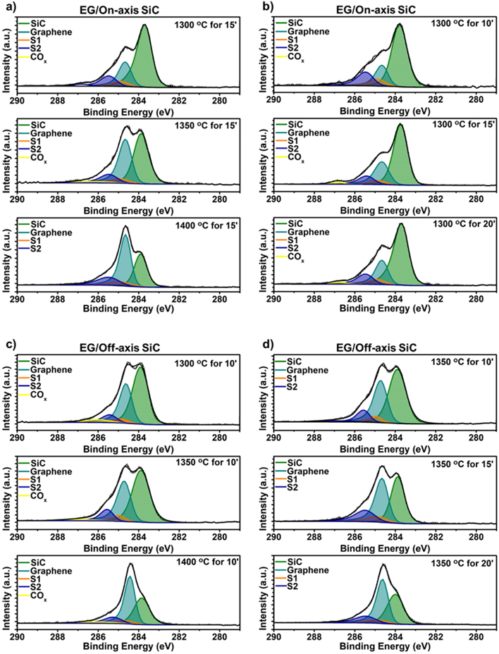
Figure 2. Chemical characterization of FTF grown epitaxial graphene. Evolution of C1s XPS core level spectra for growth of epitaxial graphene using FTF technique (a), (c) as a function of growth temperature and (b),(d) growth time on on-axis and off-axis SiC respectively. S1 and S2 are the contributions of the buffer layer.
Download figure:
Standard image High-resolution imageThe intensity ratio of the graphene component ( ) to the SiC component as a reference peak (
 ) is used to calculate the thickness of epitaxial graphene grown on on-axis and off-axis SiC using the relation [49]:
where T is the transmission function of the analyser, E is the kinetic energy of photoelectrons for graphene (EG
) and SiC (ER
) in XPS,  is the atomic density of the material, C is the differential cross section (
 ),
),  is the inelastic mean free path and
  is a geometrical correction factor caused by photoelectron diffraction. The superscript
  denotes quantities that apply to the graphene overlayer rather than the bulk SiC. The TPP-2M formula is used to calculate the estimated inelastic mean free path of graphite and SiC [50]. By calculating the thickness of epitaxial graphene
  using equation (1) and dividing this value by the graphene interlayer spacing value of 3.35 Å, the number of layers for each sample is calculated. The atomic concentration of graphene and SiC extracted from the C1s XPS peak, and the calculated number of graphene layers at various annealing temperatures and growth times are tabulated in table 1 for on-axis and off-axis SiC. From table 1 is apparent that the growth rate is higher for off-axis SiC compared to on-axis SiC. Monolayer graphene is obtained by annealing on-axis and off-axis SiC at 1350 °C and 1300 °C for 10 min respectively. As a comparison, the atomic concentration of graphene and SiC C1s components and the calculated number of graphene layers obtained with the standard growth technique are tabulated in table S1 for both on-axis and off-axis SiC. Note that in this case by annealing SiC at 1280 °C for just 1 min results in 3.87 and 2.69 graphene layers for on-axis and off-axis respectively. This proves the effectiveness of FTF growth technique in comparison with the standard method in controlling the growth rate of epitaxial graphene. The C1s XPS core level spectra of the samples tabulated in table S1 are shown in figure S1.
Table 1. Calculated number of graphene layers in FTF method. The atomic concentration of SiC and graphene components of C1s XPS core level spectra and the number of graphene layers calculated accordingly for epitaxial graphene grown by FTF technique at different growth temperatures and time on on-axis and off-axis SiC.
| On-axis SiC | Off-axis SiC | ||||||||||
|---|---|---|---|---|---|---|---|---|---|---|---|
| T (°C) | Growth time (mins) | Atomic concentration (%) | Graphene layers | Error ± | T (°C) | Growth time (mins) | Atomic concentration (%) | Graphene layers | Error ± | ||
| SiC | Graphene | SiC | Graphene | ||||||||
| 1280 | 15 | 72.82 | 8.83 | 0.31 | 0.09 | 1300 | 5 | 52.62 | 14.01 | 0.67 | 0.53 |
| 10 | 51.65 | 30.24 | 1.37 | 0.10 | |||||||
| 20 | 62.87 | 24.61 | 0.96 | 0.12 | 15 | 37.33 | 22.28 | 1.39 | 0.49 | ||
| 1300 | 10 | 70.79 | 19.47 | 0.69 | 0.17 | 20 | 49.34 | 31.37 | 1.48 | 0.12 | |
| 15 | 64.44 | 19.46 | 0.75 | 0.12 | 1350 | 5 | 42.27 | 36.14 | 1.89 | 0.13 | |
| 20 | 68.22 | 21.69 | 0.91 | 0.07 | 10 | 47.17 | 40.34 | 1.91 | 0.28 | ||
| 1350 | 5 | 63.72 | 20.55 | 0.80 | 0.15 | 15 | 37.81 | 40.42 | 2.27 | 0.42 | |
| 10 | 61.19 | 26.24 | 1.04 | 0.12 | 20 | 38.19 | 43.82 | 2.41 | 0.31 | ||
| 15 | 53.51 | 31.23 | 1.37 | 0.30 | 1400 | 5 | 47.29 | 32.02 | 1.56 | 0.28 | |
| 20 | 47.28 | 34.87 | 1.67 | 0.15 | 10 | 33.74 | 44.98 | 2.71 | 0.74 | ||
| 1400 | 5 | 66.81 | 18.62 | 0.70 | 0.15 | 15 | 31.84 | 51.66 | 3.15 | 0.55 | |
| 10 | 56.14 | 33.01 | 1.37 | 0.08 | 20 | 29.51 | 51.39 | 3.32 | 0.48 | ||
| 15 | 46.91 | 31.63 | 1.55 | 0.30 | |||||||
| 1450 | 5 | 52.64 | 32.8 | 1.44 | 0.11 | ||||||
| 10 | 39.25 | 39.82 | 2.18 | 0.65 | |||||||
| 15 | 43.14 | 33.27 | 2.24 | 0.13 | |||||||
| 1500 | 5 | 38.37 | 48.87 | 2.49 | 0.55 | ||||||
| 10 | 30.81 | 49.99 | 3.15 | 0.62 | |||||||
3. Time evolution of the growth
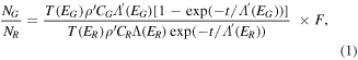
The evolution of Graphene and SiC components of XPS C1s core level spectra was investigated as a function of time at different annealing temperatures to understand the growth mechanism of epitaxial graphene. Figures 3(a) and (b) show the sample evolution of the C1s peak as a function of time for epitaxial graphene grown at 1350 °C and 1400 °C on on-axis and off-axis SiC respectively. The relative intensity of graphene and SiC components change by time and as the growth time increases, the intensity of graphene peak increases due to the development of the graphene layers.
Figure 3. XPS time evolution of FTF grown epitaxial graphene. Time evolution of XPS C1s core level spectra for epitaxial graphene grown on (a) on-axis SiC and (b) off-axis SiC at 1350 °C and 1400 °C respectively.
Download figure:
Standard image High-resolution imageHere we analyse the growth of epitaxial graphene considering the Frank Van der Merwe model which applies to the layer-by-layer growth of thin films. This model considers the evolution of epitaxial graphene when the Si atoms leave the surface and the C atoms form 2D graphene islands [51]. Defects, polishing sites and step edges of SiC are potential nucleation sites: the first 2D graphene islands start to form around these nucleation sites and increase their size to build the first graphene layer. Si atoms keep escaping step edges and the defects on the surface leading to the formation of other graphene layers on top of the buffer layer which is an interface layer partially connected to the Si atoms of SiC [52]. Considering the Frank Van der Merwe growth model, the kinetics are described by the equation:

where n is the number of layers,  is the rate constant of the process, and
  is a function of the number of layers. The function
  depends on the mechanism of the reaction which in this case involves diffusion of Si and C atoms across the solid phase for the formation of graphene. As the speed of the reaction decreases with the increase of the number of layers, we have

where b is a constant. This function accounts for the increasing difficulty of Si atoms in leaving the surface as the number of graphene layers increases. The kinetics of reaction  can be expressed as:

where  is a pre-exponential factor, Ea
is the activation energy and k is the Boltzmann constant (8.617 × 10⁻⁵ eV K−1). From equations (2) and (3) the following well-known parabolic kinetics can be obtained:
is a pre-exponential factor, Ea
is the activation energy and k is the Boltzmann constant (8.617 × 10⁻⁵ eV K−1). From equations (2) and (3) the following well-known parabolic kinetics can be obtained:

The integral of equation (5) is  and by assuming the constants as zero (n = 0 for t = 0) we obtain:

The number of graphene layers developed on on-axis and off-axis SiC by annealing at different temperatures is plotted as a function of growth time as shown in figures 4(a) and (b) respectively. The data in figures 4(a) and (b) are fitted using the following power growth law and the value of β for each temperature is determined as [53].

By using the β values as parameters of equation (6) and plotting the Arrhenius plots: ln(β) versus  (figures 4(c) and (d)), the activation energies of 4.1 ± 0.6 eV and 3.6 ± 1.3 eV are obtained for growth on on-axis and off-axis SiC respectively. The obtained β values at different temperatures are given in table 2. The activation energy values obtained in this study are similar to the values reported in our previous paper for the growth of epitaxial graphene on 3C SiC/Si(111) [54]. Concerning the activation energy extracted from the kinetics of figure 4, it is expected to be made up of several contributions. As described earlier, the formation of the graphene layers is a multi-step process involving the sublimation of Si, via diffusion through the forming layer, with generation of C atoms for the growth of the graphene phase. We proposed a kinetic approach for the graphene growth in vacuum at high temperature, by modeling Si diffusion in the layer via defects formation [54]. Specifically, the following reactions were considered for sublimation and growth


where  is a Si atom in the gas phase, C* a 'reactive' C atom and
  a graphene layer made up of n-Carbon units. The solution of the kinetics provides the time dependence of the thickness of the overlayer. Moreover, it was shown that the parabolic law (equation (7)) is attained for exp
 ![$\left[-\left({U}_{d}^{* }+\frac{{E}_{\mathrm{Si}}}{2}-{U}_{{C}^{* }}\right)/kT\right]\cong \exp \left[-\left({U}_{d}^{* }+\frac{{E}_{\mathrm{Si}}}{2}\right)/kT\right],$](https://content.cld.iop.org/journals/0957-4484/34/10/105601/revision2/nanoaca8b2ieqn18.gif) where
where  is the activation energy for Si diffusion,
  the energy for Si vacancy formation at the interface and
  the activation energy for the kinetic step (equation (9)). Accordingly, it follows that Ea, in equation (6), can be identified with
  The slight decrease of this quantity, on going from on-axis to off-axis sample, can be ascribed to the larger step density which may reduce the energy for defect formation.
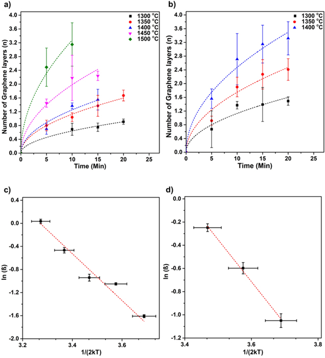
Figure 4. Evolution of the growth rate for FTF grown epitaxial graphene. Time dependence of developed graphene layers on (a) on-axis SiC and (b) off-axis SiC at different annealing temperatures. (c) and (d) correspond to the Arrhenius plots of the fitting parameter β (ln(β) versus 1/2kT) obtained from (a) and (b) respectively.
Download figure:
Standard image High-resolution imageTable 2. Calculated parameter from the evolution of growth rate analysis. Values of β obtained from the fitting of n (t) using equation (6) at different temperatures for the growth of epitaxial graphene on on-axis and off-axis SiC by FTF technique.
| T(°C) | β (min−1/2) | σ (×10–2) | |
|---|---|---|---|
| On-axis SiC | 1300 | 0.203 | 0.51 |
| 1350 | 0.357 | 0.82 | |
| 1400 | 0.396 | 2.32 | |
| 1450 | 0.627 | 2.91 | |
| 1500 | 1.035 | 3.91 | |
| Off-axis SiC | 1300 | 0.357 | 2.07 |
| 1350 | 0.552 | 2.67 | |
| 1400 | 0.782 | 2.62 |
4. Atomic force microscopy
The morphology of the epitaxial graphene grown on on-axis and off-axis SiC at different annealing temperatures and growth times has been studied by AFM in tapping mode. Figure S3 and S4 include the full set of AFM images acquired on on-axis and off-axis SiC after annealing at all the different growth temperatures and times. For epitaxial graphene on on-axis SiC, the samples with the widest terrace size are obtained at 1280 °C, 1300 °C, and 1350 °C for 20, 15 and 10 min respectively, as shown in figures 5(a)–(c). The sample shown in figure 5(b) shows the surface with the most uniform wide terraces (up to 5 μm width) covered by 0.75 graphene layers. This sample is representative of the growth in optimum conditions (1300 °C and 15 min respectively). The growth at 1300 °C for 20 min creates terraces up to 13 μm wide with 0.91 layers of graphene.

Figure 5. Morphology analysis of FTF grown epitaxial graphene on on-axis SiC. AFM topography of Epitaxial graphene on on-axis SiC grown at (a)1280 °C for 20 min, (b) 1300 °C for 15 min, and (c) 1350 °C for 10 min.
Download figure:
Standard image High-resolution imageAs the temperature increases, a shorter growth time is required to obtain one layer of epitaxial graphene. However, the samples annealed at higher temperatures show less uniform terraces with finger-like protrusions. Moreover, by increasing the annealing temperature, the density of pits and nonuniformity of steps increases as a function of growth time. Many works have reported these types of structures previously, which form due to rapid sublimation of Si [55–59]. The formation of pits can be controlled by the mechanism of growth, and it has a very strong influence on the nucleation of graphene. Here the growth of epitaxial graphene is well controlled by the FTF technique with the best results obtained at 1300 °C for 20 min (figure 5(b)). In these conditions the formation of pits is limited as the slow growth at 1300 °C allows for the formation of large domains of buffer layer which have enough time to cover the SiC steps before the first graphene layer develops. We argue that the Si counter pressure over the surface provided by the FTF technique reduces the growth rate of epitaxial graphene and helps the formation of uniform epitaxial graphene on SiC at optimum growth condition. As shown in figure S3, for growth at temperatures higher than 1300 °C, the density of pits decreases as the annealing temperature increase for a certain growth time. Formation of pits initiates by nonuniform growth of buffer layer of 6√3 structure on each SiC step of √3 structure and having the SiC steps to continue to the next terrace. By increasing the annealing temperature, the density of nucleation sites for formation of the buffer layer increases and closely tied small domains cover the surface which greatly decreases formation of pits [60, 61]. Finger-like structures appear on the steps of epitaxial graphene grown at 1400 °C for 10 min as shown in figure S3. Borovikov and Zangwill reported that the instability between the capillary smoothing forces and the roughening forces driven from evaporation-condensation and diffusion mechanism of atoms at the step edge results in formation of finger-like structures [62]. For a certain pressure, they define a graphitization temperature (Tg ) below which graphene doesn't grow and a stability temperature (Ts ) over which the growth is stable and the structure of graphene steps is uniform. For temperatures between Tg and Ts (Tg < T < Ts ) the growth is unstable and the finger-like structures form. As the background pressure in the chamber increases, the temperature window of unstable growth gets smaller up to a point where the growth is fully stable at T > Tg and Tg = Ts . This mechanism is connected to the stability between the pressure originated by the sublimation of Si from the SiC surface and the background pressure of the growth chamber which determines the average velocity of steps movement in the kinetic theory. In the present work, the epitaxial graphene growth is performed under UHV, and finger-like structures are rarely observed across the temperatures and growth times explored. Tapping mode AFM and KPFM images of a partially graphitised on-axis SiC surface prepared by FTF annealing at 1300 °C for 5 min are shown in figure S6 to show different phases of the growth on the SiC surface. Figure S7 shows the plots of the line profiles taken along an identical path from height, phase and contact potential difference (CPD) channels, corresponding to the black, blue, and red paths in figured S6(a)–(c). While variations in the graphene layer thickness are unclear in the height channel (figure S6(a)), the CPD in figure S6(c) clearly shows three contrast levels which correspond to the SiC substrate (low CPD), monolayer graphene, and bilayer or multilayer graphene (high CPD). In summary, it seems that the FTF technique has helped to effectively stabilize the growth and to control the structure of graphene steps.
Figures 6(a)–(c) shows the AFM images of epitaxial graphene grown on off-axis SiC at 1300 °C, 1350 °C and 1400 °C for 15, 10 and 5 min respectively. In this case, annealing at 1350 °C for 10 min is the optimised growth condition, resulting in 1.9 layers of graphene and terrace width of up to 440 nm which is the sample with the widest continuous steps and minimum number of graphene layers at the same time. All the AFM images of the samples grown on off-axis SiC at various growth temperatures and time show pit-free structures (figure S4). However, monolayer or bilayer graphene islands can be seen on the steps of epitaxial graphene grown at 1350 °C for 20 min (figure S5). We believe that these structures are formed when the steps of SiC retract due to decomposition. As the SiC retracts and joins the adjacent SiC step, it leaves behind the earlier formed graphene layers as islands while some of the graphene islands continue to grow. This process continues while the SiC terraces continue to retract to join other SiC steps and the nucleated graphene islands grow to form continuous graphene layers [63]. The surface morphology of epitaxial graphene grown by standard technique on on-axis and off-axis SiC by annealing at 1300 °C for 1 min are shown in the figure S2 STM images that are obtained in situ after growth in UHV system. In this technique, epitaxial graphene on on-axis SiC (figure S2(a)) shows a nonuniform and discontinuous island with defects such as pits and wrinkles. On the other hand, epitaxial graphene on off-axis SiC shows continuous but very narrow (up to 10 nm) terraces covered by wrinkles. Comparing the morphology of FTF grown epitaxial graphene with the samples grown by standard technique, it is proven that the structure of epitaxial graphene grown both on on-axis and off-axis SiC is significantly improved by FTF method in terms of uniformity, quality, and size of terraces.
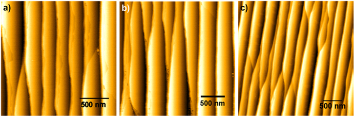
Figure 6. Morphology analysis of FTF grown epitaxial graphene on off-axis SiC. AFM topography of Epitaxial graphene on off-axis SiC grown at (a)1300 °C for 15 min, (b) 1350 °C for 10 min, and (c) 1400 °C for 5 min.
Download figure:
Standard image High-resolution image5. Scanning tunnelling microscopy
Atomically resolved STM images of epitaxial graphene grown on on-axis SiC at 1300 °C for 15 min and on off-axis SiC at 1350 °C for 10 min (optimised growth conditions) are shown in figures 7(a) and (b) respectively. The (1 × 1) graphene lattice structure is clearly visible and marked in green in the zoomed-in images (insets) in figures 7(a) and (b) The line profile along the red line indicated on both figures 7(a) and (b) is represented below each graph and shows the atomic periodicity of 0.241 ± 0.005 nm and 0.239 ± 0.005 nm respectively which closely matches the graphene lattice parameter (0.246 nm). Figure 7(a) shows the superposition of (6√3 × 6√3)R30˚ moiré pattern (blue unit cell) and graphene honeycomb lattice structure of monolayer graphene. The moiré superlattice, which arises due to the rotation of the (6√3 × 6√3)R30˚ reconstructed buffer layer with respect to the SiC(0001) substrate, has a periodicity of about 18 Å [64, 65], which is not very clear in figure 7(b) as the number of graphene layers is higher with respect to 7a and only a shadow of the Moiré pattern is visible. The FFTs of figures 7(a) and (b) are shown in figures 7(c) and (d) respectively. Both figures 7(c) and (d) show the pattern containing three sets of bright spots which correspond to (6√3 × 6√3)R30˚ (buffer layer), graphene, and the Moiré pattern. The angle between the first and the second set of spots shows the orientation of epitaxial graphene with respect to (6√3 × 6√3)R30˚. In figure 7(c) this rotation is 34° ± 0.5° with respect to the SiC substrate (on-axis SiC). For off-axis SiC, the rotation of graphene is 32.0° ± 0.2° (figure 7(d)). The observed discrepancy of rotation of graphene form 30˚ is due to the drift during the STM image acquisition. An analysis of the various components of the FFT transform (figures 7(c) and (d)) is shown in figure S8. The back Fourier Transform of the central, middle, and outermost hexagons as marked in the FFT inset images of figure S8 provide the real space image of the moiré pattern, second nearest neighbour, and first nearest neighbour atoms respectively.
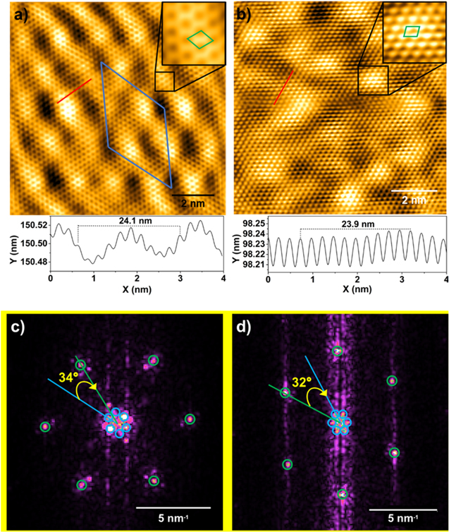
Figure 7. STM characterization of FTF grown epitaxial graphene. (10 × 10) nm2 atomic resolution STM images of epitaxial graphene grown by FTF technique on (a) on-axis SiC (U = −0.9 V; I = 0.03 nA) and (b) off-axis SiC (U = − 0.6 V; I = 0.7 nA) at optimised growth conditions of annealing at 1300 °C for 15 min and 1350 °C for 10 min respectively. (a) shows Moiré pattern with hexagonal symmetry and (6√3 × 6√3)R30° unit cell which is marked in blue. The insets show the zoom-in of the STM images with graphene unit cells marked as green. The atomic corrugation of graphene is represented by the line profiles along the red lines (c) and (d) shows the respective FFT images of (a) and (b).
Download figure:
Standard image High-resolution image6. Raman spectroscopy
Raman analysis of the FTF grown epitaxial graphene on both on-axis and off-axis SiC has been performed ex situ after the growth. The Raman spectra are shown in figure 8 and figure 9 respectively. Figure 8(a) shows the evolution of the Raman spectrum as a function of temperature for epitaxial graphene grown on on-axis SiC for 15 min. Three characteristic Raman peaks of D, G, and 2D are labelled on the spectra. The Raman peaks of epitaxial graphene and SiC overlap and as the intensity of the G and D peaks of epitaxial graphene are very small in comparison with the SiC peaks, it is very difficult to discern them. The 2D peak, however, is located at a higher wavenumber, where there are no SiC reference peaks and the changes in this peak can be easily tracked. For epitaxial graphene on SiC we cannot define the number of graphene layers simply by looking at the shape of the 2D and G characteristic peaks in the raw Raman spectra [66]. To make the G and D peaks in figure 8(a) more distinct, the Raman spectra of untreated on-axis 4H-SiC is partially subtracted from the Raman spectra of all samples as shown in figure 8(b) as suggested by Röhrl et al [67]. The D, G, and 2D peaks do not appear on the Raman spectra for epitaxial graphene grown on on-axis SiC at 1280 °C and 1300 °C for 15 min as the number of graphene layers is less than one (0.31 and 0.75 respectively). The intensity of D peak in figure 8(a) and figure 8(b) Raman spectra is very small for all samples which confirms the excellent crystalline quality of our epitaxial graphene grown on on-axis SiC by FTF technique. Figure 8(b) shows that as the number of graphene layers is increased by increasing the annealing temperature from 1350 °C to 1450 °C, the wavenumber for D peak increases from 1353 cm−1 (1.37 layers) to 1378 cm−1 (2.24 layers). The position of G peak doesn't change by temperature and is located around 1606 cm−1. As shown in figure 8(b), the intensity of G peak increases by annealing temperature and indicates increase in the number of graphene layers. The position of 2D peak shifts from 2720 to 2745 cm−1 with increase in annealing temperature and consequently the number of graphene layers from 1350 °C to 1450 °C (figure 8(a)). Figure 8(c) shows the Raman spectra as a function of growth time for growth of epitaxial graphene on on-axis SiC at 1300 °C. By comparing the Raman spectra of plain on-axis SiC with the epitaxial graphene grown at 1300 °C for 10 min, we can see that the D, G, and 2D peaks are absent as the number of layers is 0.69. As the growth time increases from 10 to 15 min (0.75 layers), no 2D peaks appear but a very low intensity G peak can be seen in the background subtracted Raman spectra (figure 9(d)). For 20 min of growth, the 2D peak appears at 2718 cm−1 (figure 8(c)) and the G and the very small intensity D peaks are seen at 1605 and 1349 cm−1 respectively (figure 8(d)). The same increasing trend for 2D peak as growth on on-axis SiC can be seen for growth on off-axis SiC in figure 9(a) and the position of this peak increases with the growth temperature. For growth at 1300 °C, 1350 °C, and 1400 °C the position of 2D peak is 2725, 2729, and 2743 cm−1 respectively. The D and G peaks are shown in figure 9(b) after subtraction SiC background for each annealing temperature. The position of G is at ∼1606 cm−1 for all the samples. The small intensity D peaks for all samples again indicate the high quality of epitaxial graphene grown on off-axis SiC. The position of D peak also increases by the number of graphene layers and by increasing the annealing temperature or the growth time (figures 9(b), (d)). The Raman spectra around the D and G peaks for epitaxial graphene grown by FTF technique on on-axis and off-axis SiC at optimised growth conditions of annealing at 1300 °C for 15 min and 1350 °C for 10 min as well as epitaxial graphene grown by standard technique on on-axis and off-axis SiC by annealing at 1300 °C for 1 min are shown in figure S9. The intensity of D peak for FTF grown epitaxial graphene on both on-axis and off-axis SiC is negligible in comparison to the epitaxial graphene grown by standard technique on on-axis and off-axis SiC. This confirms high quality of epitaxial graphene grown by FTF technique and how the presence of defects is notably diminished in this method, a clear improvement with respect to previous results. The FTF technique is a simple way to overcome two common causes of defect formation in the growth of epitaxial graphene on SiC in UHV: low growth temperature and fast Si evaporation from the SiC surface [42]. The control over the fast growth rate and sublimation of Si in UHV is achieved by the counter pressure created by Si atoms towards the surface of SiC which provides equilibrium in the sublimation process by reducing the Si evaporation rate, consequently preventing the formation of defects on the surface by slow reconfiguration of C atoms [68]. By using the FTF technique in UHV we can decrease the growth temperature and time and reduce contamination, a definite improvement with respect to previous attempts in high vacuum [45].
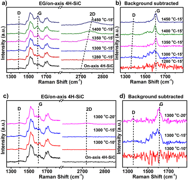
Figure 8. Raman characterization of FTF grown epitaxial graphene on on-axis SiC. The evolution of Raman spectra as a function of (a) annealing temperature and (c) growth time for FTF growth of epitaxial graphene on on-axis SiC with the on-axis 4H-SiC(0001) reference. (b) and (d) The Raman spectra around the D and G peaks for the samples shown in (a) and (c) respectively with the partial subtraction of bare SiC Raman spectra as background.
Download figure:
Standard image High-resolution image
Figure 9. Raman characterization of FTF grown epitaxial graphene on off-axis SiC. The evolution of Raman spectra as a function of (a) annealing temperature and (c) growth time for FTF growth of epitaxial graphene on off-axis SiC with the off-axis 4H-SiC(0001) reference. (b) and (d) The Raman spectra around the D and G peaks for the samples shown in (a) and (c) respectively with the partial subtraction of bare SiC Raman spectra as background.
Download figure:
Standard image High-resolution image
7. Conclusion
A novel FTF growth technique is explored to control the growth of epitaxial graphene in UHV condition. The growth on both on-axis and off-axis SiC is optimised and the best annealing temperature and growth time are reported. Epitaxial graphene grown on on-axis SiC at 1300 °C for 15 min shows the most uniform and widest terraces (up to 5μm). The growth on off-axis SiC at 1350 °C for 10 min shows the widest terraces (up to 440 nm). The FTF technique proves to be very effective in controlling the growth rate and structure of epitaxial graphene under UHV by decreasing the rate of Si sublimation from the surface via the counter pressure generated by Si sublimation in the space between the two SiC substrates. The number of graphene layers is calculated for each annealing temperature using quantitative XPS analysis and a growth model has been used to describe the evolution of the number of layers as a function of time. The square root growth law obtained by fitting our data is an indication of the layer-by-layer growth of epitaxial graphene. According to this law, the kinetic model shows that the rate declines as a function of time because the development of graphene layers hampers fast sublimation of Si, by limiting the pathways for the sublimation of Si which occurs normally via defects and step edges. The activation energies are calculated based on the kinetic model as 4.1 ± 0.6 eV and 3.6 ± 1.3 eV for the growth on on-axis and off-axis SiC respectively. High resolution STM images show the high quality of graphene and the superposition (6√3 × 6√3)R30˚ moiré pattern. The evolution of D and 2D peaks in Raman spectroscopy are studied as a function of temperature and time. The very low intensity of D peaks in the Raman spectra of all samples confirms the high quality of graphene grown by the FTF technique.
The growth by the FTF technique provides an effective solution to obtain high-quality epitaxial graphene on SiC in UHV, paving the way to its applications in 2D electronics.
Acknowledgments
NZ acknowledges the support from Australian Government Research Training Program (RTP). Facilities at Central Analytical Research Facility (CARF) and the Faculty of Science and the Faculty of Engineering that provide funding for all the research facilities in CARF are kindly acknowledged. The authors acknowledge the facilities and support provided by Australian National Fabrication Facility (ANFF) at University of Queensland (UQ). This work has been partially supported by ARC through the Discovery Project DP200102546.
Data availability statement
The data that support the findings of this study are available upon reasonable request from the authors.
Supplementary data (0.8 MB PDF)