
Abstract
Materials exhibiting an exchange bias effect are a class of magnetic systems that have a wide range of possible technological applications e.g. in sensors, read heads, and spintronic devices. In this study, we demonstrate the effect of laser interference patterning on the magnetic properties of Pd/CoO/Co/Pd multilayers. Laser patterning creates arrays of well-ordered stripes, rectangles, and squares on the substrate surface. We found that the laser treatment caused magnetic softening of the structure edges while the centers of the objects remained unchanged and exhibited the exchange bias effect. In this study we focused on the shape and configurational magnetic anisotropies induced by patterning and showed that the magnetic properties varied depending on the angle at which the external magnetic field was applied with respect to the pattern geometry.
Export citation and abstract BibTeX RIS

Original content from this work may be used under the terms of the Creative Commons Attribution 4.0 licence. Any further distribution of this work must maintain attribution to the author(s) and the title of the work, journal citation and DOI.
1. Introduction
Exchange bias is a magnetic effect which appears at the interface between a ferromagnet and an antiferromagnet and causes a shift of a magnetic hysteresis loop along the external field axis [1]. This loop shift is called the exchange bias field Hex and occurs after the cooling of the system through Néel temperature of the anitferromagnet in the external magnetic field larger than the saturation field of the ferromagnet. The microscopic origin of this effect remains unclear; however, some reports describe the phenomenology behind this effect by considering the domain state model [2], the role of the interfacial spins [3], and roughness of the ferromagnet–antiferromagnet interface [4]. On the other hand, materials exhibiting this effect found technological application in sensors [5, 6], magnetic read heads [7], spintronic devices [8–10], or as shape memory alloys [11].
In this paper, we present research on the laser-patterned Pd/CoO/Co/Pd multilayer. The patterning was done using Direct Laser Interference Lithography which is a fast and easy to apply surface structurization method and can be used for metallic films [12–17], as well as for non-metallic materials [18–21]. In this method, the sample is irradiated with at least two laser beams generating an interference pattern on its surface. In case when the laser beam energy is large enough, the temperature generated at the interference maxima is sufficient to remove the material through the thermal ablation process. On the other hand, in places of the interference minima the material remains intact since temperature is too low to cause any structural changes. The patterning is usually done using a single laser shot with duration time in the range of nanoseconds. Shape, size, and periodicity of obtained pattern are dependent on the geometry of the optical system and the laser wavelength. The main advantage of the laser patterning method is its fastness. The method is a one step process after which the pattern is produced at the same time over whole exposed surface. It does not require mechanical masks or chemical etching like in conventional optical lithography [22], or precise scanning with an optical/electron beam [23]. Moreover, after the patterning the produced structures are aligned accurately in the same direction over the entire illuminated area which is hard to replicate using techniques like nanosphere litography [24] or surface anodization [25] where the structures are well oredered within structural domains which, in turn, may be misaligned with each other. This property of the laser patterning, the excellent geometrical pattern arrangement, is essential for the investigations of the shape-dependent magnetic anisotropy investigations where the external magnetic field is applied parallel to the structurized surface.
Here, we applied this type of patterning to study in-plane angular dependence of the exchange bias field and coercivity on the structure shape and size of the Pd/CoO/Co/Pd system. We chose the CoO-Co antiferromagnet–ferromagnet interface since it is a model case for investigations of different aspects of the exchange bias effect [26–31]. The influence of the lattice geometry on the magnetic properties of thin films was previously studied for ferromagnetic antidot array structures [32]. Angle-dependent experiments on exchange-biased systems were also done by Tripathy et al for elongated nanorings [33] and antidots [22]. However, in these studies the exchange bias effect was induced by depositing magnetic systems in the presence of a constant in-plane magnetic field which determined the reference spatial direction for further magnetic measurements. A related experiment with a fixed magnetic pinning direction was also performed on a flat multilayer [34]. In our study, we focused on the magnetic shape and configurational anisotropies of the periodical assemblies of stripes, squares, and large and small rectangles with sizes and periodicities of several microns.
2. Experimental
Samples were prepared by thermal evaporation in the ultra-high vacuum chamber under the pressure of 10−7 Pa at room temperature on the Si(100) single crystal substrates. First, a 2 nm thick Pd buffer layer was deposited to separate the multilayer from the native SiOx oxide on the surface of the substrates. Then, a Co layer with thickness of 1.5 nm was evaporated at the rate of 5 Å min−1. Next, the Co layer was oxidized for 10 min in the pure oxygen atmosphere at the pressure of 3 × 10² Pa to obtain a cobalt oxide layer. After that, the next layer of pure Co with thickness of 4 nm was deposited to establish the antiferromagnetic–ferromagnetic CoO/Co interface. Finally, the multilayer was covered by 2 nm of Pd to prevent further oxidation. All samples were 3 mm × 3 mm in size and were prepared in one deposition process.
Laser patterning was carried out using Quantel Nd:YAG pulsed laser operated at wavelength of 532 nm with pulse time of 10 ns. Energy density of a single pulse was 14 mJ cm−2. The laser was equipped with an injection seeder to provide long radiation coherence length. The geometry of the irradiation experiment is schematically shown in figure 1. The beam coming from the laser was pointed at the first mirror and directed towards a 50:50 beam splitter. Half of the beam was reflected and aimed at the sample. The other half which passed through the beam splitter was pointed at the second mirror and then directed towards the sample. The distance a between the beam splitter and the second mirror was 2 cm and it was constant during the experiments. The two source laser beams were focused and met each other at the multilayer situated at a distance b from the plane established by the beam splitter and the second mirror. This led to the occurrence of the periodic interference pattern on the specimen. The laser energy density was large enough to ensure the material removal from the places of the interference maxima due to thermal ablation and, at the same time, it was too low to induce morphology changes in the Si substrate [21]. The periodicity of the interference pattern d can be calculated according to the equation [16]:

and the angle Θ = arctg(a/2b). We performed three types of experiments for different distances b. In each case, when the position of the sample was changed, the beams were focused at the multilayer surface giving different values of the angle Θ.
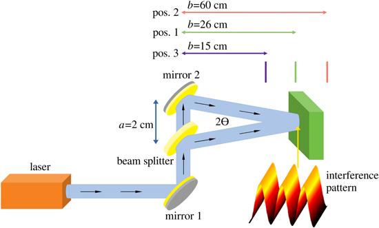
Figure 1. Schematic representation of the laser setup used in the irradiation experiments.
Download figure:
Standard image High-resolution imageIn the first experiment, the CoO/O system was placed in position 1 at the distance b = 26 cm with angle Θ = 2.2°, and irradiated with a single laser shot. According to equation (1), this should lead to creation of the pattern of stripes with periodicity of 7 μm. In the second experiment another sample was irradiated in position 1 with two pulses, and between the laser shots the sample was rotated by 90° to produce an array of squares with the same periodicity as for stripes. In the third experiment, another sample was illuminated in position 1, and then rotated by 90° and moved to position 2 where the distance b was 60 cm and the angle Θ = 0.95°. This, according to equation (1), should result in creation of the pattern of large rectangles with periodicities of 7 μm and 16 μm along two perpendicular directions. In the last experiment, the CoO/Co system was first irradiated in position 1, rotated by 90°, and then illuminated in position 3 with distance b equal 15 cm and the angle Θ = 3.8°. This procedure lead to formation of pattern consisting of small rectangles with expected periodicities of 7 μm and 4 μm along the perpendicular directions as calculated from equation (1). One sample was left as an unirradiated flat reference. In each case, the whole sample area was covered by the laser spot and illuminated.
The multilayer structure of the flat unirradiated sample was investigated by x-ray reflectivity method. The measurement was carried out for the scattering angle ω from 0.2° to 3°, using an X'Pert Pro PANalytical diffractometer equipped with Cu x-ray tube operated at 40 kV and 30 mA. Data were fitted using PANalytical X'Pert Reflectivity software utilizing the Parrat algorithm. Magnetic hysteresis loops were measured using the Quantun Design MPMS XL SQUID magnetometer. The loops were recorded in in-plane geometry at 10 K. To induce the exchange bias effect the samples were cooled down in the external magnetic field of +50 kOe prior to each hysteresis measurement. The scanning electron microscopy (SEM) imaging was carried out using the Tescan Vega 3 SB device at the electron beam energy of 3 keV.
3. Results
The multilayer structure of the flat system was investigated using XRR technique and the results, together with the numerical fit, are presented in figure 2. The total multilayer thickness calculated from the fit is 11 nm. Both seed and capping Pd layers have assumed thicknesses of 2 nm. The thickness of the oxidized cobalt layer was calculated for 3 nm which was formed from initially deposited 1.5 nm of pure Co. The expand of the oxidized cobalt layer is associated to the oxygen atoms incorporation in the metallic layer and it was previously observed in other reports [27, 35–37]. Density of this layer was 6.4 g cm−3 which is close to the bulk value for CoO equal to 6.44 g cm−3. Therefore, it can be expected that we produced the CoO layer, and the material has suitable antiferromagnetic properties for being magnetically coupled to the ferromagnetic Co layer and to give rise to the exchange bias effect. The thickness of the Co layer, deposited on the top of CoO, is 4 nm which stays in agreement with its nominal value, and its density matches the bulk value. The root mean square roughness of the CoO/Co interface, calculated from the numerical fit, is 1.1 nm. This value is considerable in comparison to the thickness of the CoO layer which is due the oxidation procedure applied to obtain an antiferromagnetic oxide. The Pd/CoO and Co/Pd interfaces have thicknesses of approximately 0.9 nm.

Figure 2. X-ray reflectivity results for the flat unirradiated Pd/CoO/Co/Pd multilayer. Blue circles are the experimental points, red line is the numerical fit.
Download figure:
Standard image High-resolution imageThe structures obtained by the laser irradiation were studied by the means of scanning electron microscopy (SEM). For more clarity, we adopt the convention where the direction along which the period is constant and equal to 7 μm (across the stripes produced by the first laser pulse) is denoted as horizontal (h), while the perpendicular direction (along the initial stripe pattern) is referred as vertical (v). Representative SEM micrographs of the patterned samples, together with the vertical and horizontal structure cross-sections and the structure size distributions, are presented in figure 3.

Figure 3. Representative SEM micrographs (upper row), horizontal and vertical cross-sections (middle row), and structure size histograms with fitted log-normal distributions (lower row) for the patterns of (a) stripes, (b) large rectangles, (c) squares, and (d) small rectangles. In the SEM images the CoO/Co multilayer are light gray while the Si substrate is dark. The insets in the SEM images show 2D Fourier transforms of the micrographs. The magnetic surface coverage ratios S in [%] are indicated in the images. In the cross-sections, the lattice periodicities are marked with gray arrows, and the vertical L and horizontal W structure sizes are indicated with color arrows. The single structure area calculated from the log-normal fit  and by multiplication of the horizontal and vertical structure sizes AW×L
are all given in the histograms.
and by multiplication of the horizontal and vertical structure sizes AW×L
are all given in the histograms.
Download figure:
Standard image High-resolution imageA careful SEM inspection in various locations on the patterned samples showed that approximately 90%–95% of their surface is uniformly covered with the objects produced by the interfering laser beams. The periodic fine arrangement of the objects is confirmed by the 2D Fourier transforms. The first irradiation of each sample was done in position 1, therefore, the horizontal period for all samples is 7 μm. The vertical periods, generated by the second irradiation, are 16 μm for large rectangles, 7 μm for squares, and 4 μm for small rectangles. These periodicities stay in agreement with the caltulations done using equation (1). Patterned objects have nearly rectangular cross-section shape with flat tops and spaces between the objects (figure 3, middle row). The cross-section shape of the patterns is a direct consequence of a carefully chosen laser beam energy density. The flux of 14 mJ cm−2, comparable to the one used by Zheng et al [38] for patterning of Co–C films, was experimentally selected to generate temperature sufficiently high in the interference maxima to fully ablate the metallic thin film. On the other hand, it was low enough in order to not induce any significant structural and morphology changes in the interference minima to preserve multilayer structure of the film with desired magnetic properties. Additionally, the flux was decisively too low to pattern silicon substrate [21]. Such approach ensured sharp edges of objects with flat tops and flat spaces between them. According to the cross-section profiles, the horizontal sizes W of the obtained structures measured across their centers and along their top flat surfaces range from 4.4 μm to 4.6 μm while their vertical lengths L are 9.1 μm for large rectangles, 4.5 μm for squares, and 2 μm for small rectangles.
The object area AW×L , calculated by multiplying horizontal and vertical sizes W and L, is 41 μm2 for large rectangles, 20 μm2 for squares, and 9 μm2 for small rectangles. However, these values are over-estimated due to the rounded corners of the objects observed in the SEM micrographs. This effect resulted from the thermal energy dissipation process taking place in the irradiated material. To obtain more accurate results we calculated the distributions of object area A from the SEM images, and fitted them using the log-normal distribution (figure 3, lower row)

where  is the median of the distribution and σ is a dispersion of the function. The mean values
  of the object area, calculated as
  and corresponding to the maxima of the distributions, are 39 μm2, 18 μm2, and 6 μm2 for the large rectangles, squares, and small rectangles, respectively, and are smaller than those calculated using W and L lengths, as expected. Regardless the size of the structures, the dispersion σ was equal to 0.09 in each case.
The SEM analysis also showed that the percentage of the magnetic surface coverage S, defined as the ratio between the area occupied by the patterned objects to the total sample area, rises from 34% to 43% as the objects become smaller. Further analysis of the micrographs allowed to determine areal density of the objects as 82 structures per 104 μm2 for the large rectangles, 197/104 μm2 for the squares, and 465/104 μm2 for the small rectangles.
The in-plane hysteresis loops for the patterned samples measured at 10 K after field cooling in +50 kOe are presented in figure 4. In the experiments, the external in-plane magnetic field was applied in the vertical and horizontal direction with respect to the pattern geometry. The shape of the loops suggests that each system consists of two magnetic phases. The magnetization reversal of the soft phase occurs for the low external magnetic field while the switching process of the hard phase is observed for higher fields. The quantitative information about magnetic properties of these two magnetization components were received by fitting each hysteresis branch by a sum of two arctan functions reflecting the contributions of two corresponding magnetic phases to the overall hysteresis loop using the following expression [29, 30, 39, 40]:
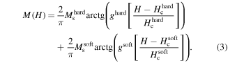
The  and
and  are the coercive fields associated with hard and soft magnetic phases,
  and
and  are their saturation magnetizations, and ghard and gsoft are parameters related to the curve slope. The coercive field of the soft phase ranges from 200 Oe to 400 Oe with no bias field, its saturation magnetization increases as the patterned objects become smaller, and the magnetic remanence is 0.3–0.4 of the
  value. The hard component shows larger coercivity with the loop shift along the external field axis indicating the presence of the exchange bias effect. The hard loops demonstrate large magnetic remanence of approx. 0.9
  , and their saturation magnetizations decrease proportionally to the rise of the soft component contribution as the size of the structures decreases.

Figure 4. In-plane hysteresis loops for the patterned samples measured at 10 K after field cooling in +50 kOe. The loops showed in the upper row were measured with the external magnetic field applied in horizontal direction, while the lower row shows loops with the field applied in vertical direction (see text). Gray circles are the experimental data and black solid lines are fits. The soft loops are indicated with yellow fields while the hard loops are marked with colors (see text). The insets show the orientation of the external magnetic field with respect to the pattern geometry.
Download figure:
Standard image High-resolution imageThe existence of the soft component without the bias field is linked to the appearance of the damaged structure edges with altered magnetic properties which developed as a result of the patterning process. The structure edges were exposed to high temperature generated by the laser beam in the interference maxima which induced material intermixing and oxidation followed by the structural and magnetic changes. Similar findings on the structure edges becoming magnetically softer upon various patterning procedures were reported in case of nanosphere lithography [24, 29], ion or electron beam lithography [41, 42], films on anodized alumina oxide [43, 44], or nanoimprinted dots [45]. Since the laser beam energy density was fixed, we assume that the thickness of the damaged edges is constant and does not depend on the structure size [29]. Therefore, the ratio between the material volume in the unaffected structure centers and the volume of the damaged edges becomes higher as the structure size decreases. This leads to gradual rise of the soft phase contribution to the overall magnetization as observed in the hysteresis loops. Besides the edges, the material within the structures remained unaffected by the laser beam. This allowed exchange coupling between the antiferromagnetic CoO and ferromagnetic Co layers which gave rise to the hard hysteresis loop component exhibiting the bias shift.
Figure 5 shows the dependencies of the exchange bias field ∣Hex∣ and coercivity Hc of the hard magnetization component measured in vertical and horizontal directions on the areal structure density and the structure area  . Qualitatively, the changes of the ∣Hex∣ follow the evolution of the coercive field. We observed that for the pattern of stripes both ∣Hex∣ and Hc fields are larger than for the reference flat sample. Similar findings were presented by Nemoto et al [46] for exchange-biased wires and it was associated with the altered size of the antiferromagnetic domains in a pattern system with respect to a flat one. Additionally, in this case the bias field is the same in both field geometries, as is the Hc. After application of the second laser pulse, for the patterns of large rectangles, we observed diminished values of both ∣Hex∣ and Hc as compared to the flat and stripe-patterned systems. On the other hand, as the structures become smaller in size (squares and small rectangles) the ∣Hex∣ and Hc fields rise. Additionally, as the objects get smaller in size they are closer to each other in the vertical direction which results in an increase of their areal density.

Figure 5. Dependencies of the exchange bias field ∣Hex∣ (upper panel) and coercivity Hc (lower panel) on the areal structure density and the structure area  , calculated from the hard magnetization component hysteresis loops, measured with the external field applied in horizontal (triangles) and vertical (squares) directions. Magnetic surface coverage ratios S are marked in red. Dashed lines are the guide for an eye.
Download figure:
Standard image High-resolution imageIt is observed for the patterns of large and small rectangles that the coercivity is larger for the case where the external field is applied along the shorter side of the object (horizontal direction for large and vertical for small rectangles). On the other hand, for these patterns the exchange bias field is larger along the longer side of the particles. In case of the pattern of squares there is no substantial difference in the Hc and ∣Hex∣ values between the vertical and horizontal measurement geometries.
To get a deeper insight into influence of the pattern shape and geometry on the magnetic properties of the films we performed a series of the in-plane hysteresis loop measurements with the external field applied at various angles with respect to the pattern geometry. Figure 6 demonstrates the angular dependencies of the coercivity and the exchange bias field obtained for the hard magnetization components recorded in the hysteresis loops. The Hc and ∣Hex∣ were normalized to the smallest value in the data series. It was shown for an exchange-biased continuous flat film [22] that the angular dependence of Hc has a 2-fold symmetry driven by the uniaxial anisotropy. The angular dependence of Hex has a period of 360° (period of 180° for ∣Hex∣) related to unidirectional anisotropy induced by the ferromagnet–antiferromagnet coupling. However, in that experiment the magnetic system was deposited in the presence of a constant in plane magnetic field and its spatial orientation set a specific reference direction for the angular investigations of the anisotropies. In our case, prior to each hysteresis measurement, the systems were cooled down through Néel temperature with the presence of a constant magnetic field applied at a specific in plane direction. Therefore, for every hysteresis measurement the direction along which the external field was applied was parallel to the direction of the cooling field inducing the exchange bias effect. For this reason, for the flat reference sample there was no change in the coercivity and bias field with the in plane angle. This type of isotropic in-plane magnetic behavior is also observed for the pattern of stripes (figure 6(a)). In this case, since the stripes are as long as the substrate and can be considered semi-infinite, the domain wall propagation along the stripes extorted by the external magnetic field takes place in the same way as for the flat film. A slight increase of the Hc and ∣Hex∣ values (see figure 5) in comparison to the reference film can be associated with the presence of the thermally damaged structure edges originating from the patterning procedure. These edges act as pinning sites slightly hindering the magnetization reversal process and making the domain wall movement more energetically demanding and contributing to the coercivity and the bias field rise.
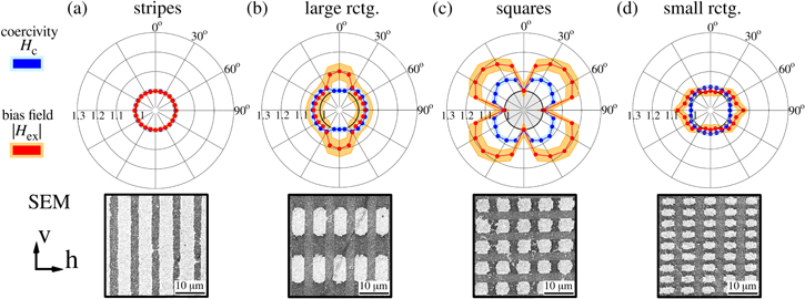
Figure 6. The in-plane angular dependencies of coercivity (blue) and the exchange bias field (red) for the patterns of: (a) stripes, (b) large rectangles, (c) squares, and (d) small rectangles. The Hc and ∣Hex∣ were normalized to the smallest value in the data series. The light blue/orange areas mark the uncertainties. The data were taken in the range 0°–90° and plotted four times to complete the circle. The low row shows the SEM micrographs to indicate the orientation of the objects with respect to the magnetic field.
Download figure:
Standard image High-resolution image
For the patterns of large and small rectangles the angular dependencies of coercivity have 2-fold symmetry (figures 6(b) and (d)), and the lowest values of Hc are observed for the external magnetic field applied along the longer sides of the objects. This behaviour is due to the magnetic shape anisotropy occurring in the structured magnetic materials and associated with the demagnetising field that tends to minimise the surface area of the magnetic poles [47, 48]. Closing the magnetic stray field lines in such a way that minimises the overall system energy and, in case of rectangular-shaped objects, makes the direction along the longer side the easy axis of magnetisation.
In both cases of rectangular-shaped objects (figures 6(b) and(d)) the angular maxima of the exchange bias field are shifted by the angle of 90° with respect to the coercivity dependencies. The easy magnetisation axis is the direction along which the antiferromagnet–ferromagnet coupling becomes more pronounced than for other angles. Since the unidirectional orientation set by the cooling field is always parallel to the measurement direction, this result may be attributed to shape anisotropy of the objects. The geometrical conditions in which the system reaches its energy minimum favours the exchange coupling.
The magnetic shape anisotropy is described by a second-rank Cartesian tensor and can be used for patterns with 2-fold symmetry. For the patterns with 4-fold symmetry Cowburn et al [47, 48] introduced a concept of configurational anisotropy deriving from slight alterations of the uniform magnetisation in structured magnetic materials. In our case, for the pattern of squares (figure 6(c)), the angular dependence of coercivity has a 4-fold symmetry with the coercivity maxima along the square diagonal and the easy magnetisation axis lying along the square side. This stays in agreement with the theoretical predictions [49, 50] and the experimental findings [48].
Tripathy et al [22] have also reported on the angular dependencies of the exchange bias field and coercivity for the pattern of circular antidots with square geometry. In this study, coercivity has a 4-fold symmetry, and the bias field change has the period of 360° (180° for ∣Hex∣) similar to that observed by the authors for the flat biased film. The coercivity dependence was connected to the configurational anisotropy, and the behaviour of Hex was related to the unidirectional anisotropy governed by the magnetic field at which the systems were deposited. In our study, the angular dependence of the bias field for the pattern of squares (figure 6(c)) has a 4-fold symmetry and the maxima are observed for the same angles as for coercivity. This may suggest that the configurational anisotropy present in our system is also the strength of the coupling between the ferromagnet and the antiferromagnet.
4. Summary
In this paper, we focused on the magnetic properties of the exchange-biased Pd/CoO/Co/Pd multilayer with the special attention paid to the shape and configurational magnetic anisotropies. We produced four types of patterns—stripes, large rectangles, squares, and small rectangles, with the sizes and periods in the range of a few micrometers. The application of this patterning method led to the appearance of the soft unbiased magnetic phase attributed to the thermally altered material present at the edges of the structures. The centers of the patterned objects were not affected by the laser beam and the material within them gave rise to the exchange-biased hard magnetic component recorded in the hysteresis loops. We observed that as the structures became smaller and got closer to each other the exchange bias field and coercivity increased. The hysteresis loop measurements performed with the external magnetic field applied at various in-plane angles showed the influence of magnetic anisotropies on the properties of the multilayer system. In case of large and small rectangles, we found that the direction along the longer side of an object is an easy axis of magnetisation which was related to the shape anisotropy exhibited by the samples. Such easy axis orientation influenced the ferromagnet–antiferromagnet exchange coupling, resulting in the largest exchange bias field observed for this direction, shifted for 90° with respect to the coercivity maxima. On the contrary, for the pattern of squares, the configurational anisotropy caused that the maxima of coercivity and the bias field to be recorded at the same angle, along the square diagonal being at the same time the hard axis of magnetization.
Data availability statement
The data that support the findings of this study are available upon reasonable request from the authors.