

Abstract
Porous ZnO nanosheets with different thickness were prepared on zinc substrate by air cold plasma for photocatalytic degradation and photoelectrochemical water splitting. The ZnO nanosheets consisted of nanocrystallines with high-density oxygen-related defects characterized by the strong red luminescence. The UV absorption tended to be saturated as the thickness increased, and the saturation occurred at a thickness of about 2.3 μm. Under UV irradiation (365 nm), the 2.3 μm thick sample with higher content of oxygen vacancies and oxygen interstitials showed the highest photocatalytic activity (and higher than P25 TiO2) in degradation of gaseous ethyl acetate. Due to the excellent UV–vis absorption ability and the effective transfer of photogenerated carriers, the ZnO nanosheets with thickness of 3.3 μm showed a photocurrent density as high as 0.22 mA cm−2 at −0.28 V (versus Ag/AgCl) under AM 1.5 G 100 mW cm−2.
Export citation and abstract BibTeX RIS
1. Introduction
Nanostructured ZnO as chemically and thermally stable n-type semiconductors have been widely applicated in photocatalytic degradation [1] and photoelectrochemical (PEC) cells [2]. In recent years, photocatalytic activities of ZnO have been improved through morphology control [3], element doping [4], application of catalyst [5], surface passivation [6], decoration with plasmonic metal nanoparticles [7], construction of heterojunction [8] and synergy of these methods [9] or other strategies [10, 11]. Preparing pristine ZnO photocatalysts with high catalytic activities and stability is of great importance because they have significant effects on the photocatalytic performance of their composites [12] and doped ones [13].
Most photocatalysts used for photocatalytic degradation are based on nano and micro-crystalline powders which provide high surface area and high quantum yield [14], such as P25 TiO2 [15] and ZnO nanoparticles [16]. However, the direct application of powder is usually accompanied by the need to filter and separate the powder from the processed liquid or gas [14]. Hence photocatalyst powders have to be securely immobilized onto certain supports. In the field of PEC water splitting, ZnO has been widely explored over the past years [17]. For example, under 100 mW cm−2 illumination (AM 1.5), ZnO nanowires showed a photocurrent of 0.017 mA cm−2 at 1.0 V (versus Ag/AgCl) [4], ZnO nanopencil arrays yielded an elevated photocurrent of ∼1.3 mA cm−2 at 1.0 V (versus Ag/AgCl) [18]. In addition, porous ZnO was another widely used structure in PEC water splitting due to the increased specific surface area (SSA) and enhanced light absorption ability [19–21]. Generally, ZnO films are synthesized by various techniques such as vapor-phase deposition [22, 23] and its modifications [24, 25], hydrothermal growth [26, 27], electrochemical routes [20, 28], and chemical bath deposition [19, 29]. However, these methods have certain limitations, such as requiring a vacuum environment, time-consuming, or involving the disposal of waste liquids. A synthesis method for nanostructured ZnO on a substrate that breaks through the aforementioned limitations is needed, and when used in PEC water splitting, the substrate should be conductive. Under this consideration, on one hand, zinc with both good chemical reactivity and exellent conductivity can be used as the raw material and the substrate at the same time for ZnO nanostructures. For example, a variety of ZnO nanostructures have been prepared by strategic low-temperature oxidation of Zn thin films in water [30–32]. On the other hand, non-thermal atmospheric pressure plasma processes have become the most promising alternative system for thermal chemical vapor deposition or wet chemical processes for the deposition of functional coatings, depending on their advantages such as low cost, low temperature, easy implementation, and in-line process capabilities [33]. For example, metal oxide nanostructures have been synthesized through atmospheric pressure plasma-based processes with metal salts [33, 34] or metals [35, 36] as precursors. In particular, the zinc-air cold plasma method has been reported as a convenient method for preparing porous ZnO nanosheets on zinc substrate [37].
In this paper, ZnO nanosheets with different thickness were fabricated by the zinc-air cold plasma method. The structural, optical absorption and photoluminescence properties were studied, and the performances in the photocatalytic degradation of gaseous ethyl acetate (with Degussa P25 TiO2 as control) and PEC water splitting were investigated. It is observed that the ZnO nanosheets exhibit a strong and broad red emission under excitation at 325 nm, which is relate to the high-density oxygen vacancies and oxygen interstitials. These defects can not only trap the photogenerated carriers to prevent recombination of excitons but also yield active sites in the photocatalytic degradation. Accordingly, the ZnO nanosheets with thickness of 2.3 μm which have higher content of above defects achieve the best perfomance in photocatalytic degradation. Whereas the ZnO nanosheets with thickness of 3.3 μm show the highest photocurrent density in the PEC water splitting, ascribed to the best visible-light absorption ability.
Compared with conventional techniques mentioned earlier, this technique for fabricationg ZnO photocatalyst films does not involve disposal of waste liquid and construction of sealed or low-pressure environments, having a simple process with a high speed of film formation [37]. Moreover, the power consumption during the discharge is low (few watts), and the raw material is only zinc foil, so the technique possesses a cost advantage.
2. Experimental
2.1. Preparation of the ZnO nanosheets
The method was reported in detail in our previous work [37]. Briefly, by exposing the zinc foil to cold plasma of the ambient air, nanosheets of calcinable zinc salt formed on the zinc surface. Porous ZnO nanosheets were then obtained by calcining the zinc salt. In the current work the discharge device is shown in figure 1(a), composed of a 1mm thick glass sheet, a 2 mm thick ceramic plate, a 0.2 mm thick zinc foil (7 cm2, purity ≥ 99.99%) and copper adhesive tapes. Discharge was driven by a sinusoidal voltage of 16.7 kV at a frequency of 5 kHz (Trek, MODEL 615-10, USA). During discharge, the ambient temperature was kept at 20 °C–22 °C and the relative humidity was maintained at 35%–40%. A filamentary discharge occurred as shown in lower part of figure 1(a). The discharge current (figure 1(b)) was monitored by a resistor (110 Ω) connected in series with the device. With a capacitor of 19 nF, the discharge power was calculated as 1.7 W by Lissajous figure [38]. Samples were finally calcined at 250°C in air for 1 h. The samples by 120, 240 and 360 s discharge were named Z120, Z240 and Z360, respectively.
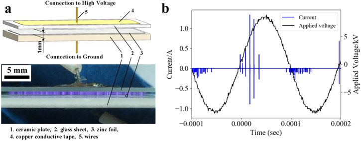
Figure 1. (a) 3D model of the discharge device and photograph at work with a exposure time of 80 ms. (b) Typical discharge current and applied voltage.
Download figure:
Standard image High-resolution imageAs a control, the TiO2 coating was prepared by the doctor blade technique [39]. TiO2 powder (Degussa P25) with the weight ratio of anatase and rutile being about 80:20 were first dispersed into the mixture of the same mass of water and ethanol to form a 10 wt% colloidal solution. Then, two adhesive tapes (about 35 μm thick) were affixed onto a zinc substrate in parallel, and a coating was finally obtained with the colloidal solution at a spread speed of 8 mm s−1. The coating was dried at 70 °C and named P25.
2.2. Characterization
Grazing incidence x-ray diffraction (GIXRD) were carried out on 3 kW/*D8 ADVANCE Da Vinci (Cu Kα, λ = 1.5406 Å). Morphologies were studied by a field emission scanning electron microscopy (FE-SEM, Carl Zeiss Ultra 55, Germany) equipped with energy dispersive x-ray spectroscopy. The crystal structures were detected by a transmission electron microscope (TEM, Talos F200x G2) and selected area electron diffraction (SAED). The porosity of the samples was studied by nitrogen adsorption–desorption isotherms on a Quantachrome autosorb IQ3. Ultraviolet–visible light diffuse reflectance spectroscopy (UV–vis DRS) and PL spectra were recorded by Perkin-Elmer LAMBDA 950 and fluorescence spectrophotometer (FLS1000, Edinburgh, UK) at room temperature, respectively.
2.3. Photocatalytic and PEC performances evaluation
The photocatalytic activity tests were carried out on a batch reactor, which was a 1.18 l aluminum cavity (13 cm × 13 cm × 7 cm) with a quartz top, a gas inlet, a gas outlet and a sampling port. Ethyl acetate (EA) was used as the model pollutant. An UV-LED lamp (365 ± 5 nm) was used as the light source, which enabled the bottom of the reactor to obtain a power density of 24 mW cm−2. Before tests, samples with total area of 21 cm2 were put at the center of the bottom of the reactor. Synthetic contaminated air with 100 ppm EA (water less than 1 ppm, Shanghai Weichuang Standard Gas Analytical Technology Co., Ltd.) was introduced into the reactor through the gas inlet. The gas inlet and outlet were closed when the concentration at the outlet was equal to that of the inlet. After the EA concentration in the reactor reached the equilibrium of adsorption and desorption within 60 min, the initial EA concentration was 100 ± 3 ppm. Then the lamp was turned on and the photocatalytic degradation started. Gas sample of 1 ml was taken for GC analysis at every 15 min interval from the reactor, for a period of 2 h. The EA concentration was determined by GC with a flame ionization detector (Shimadzu GC-2018, equipped with a Rtx-1 column). Degradation byproducts at 2 h were analyzed using GC-MS system (7890B-5977B, Agilent technologies).
PEC measurements were performed on an electrochemical workstation (CHI 660E, CH Instruments Co., China). A quartz cell was used, including the ZnO nanosheets as the working electrode, a commercial Ag/AgCl (3 M KCl) reference electrode, and a Pt foil as the counter electrode. Samples of 1 cm2 area were illuminated by simulated solar light from a Xe lamp (CEL-S500, AuLight, Beijing) with an AM 1.5 G filter. The light intensity was adjusted to 100 mW cm−2 , which was determined by the optical power meter (PM100D, THORLABS) with a S314C power probe. A solution of 0.5 M Na2S·9H2O (Rhawn, China) was used as the electrolyte. The linear sweep voltammogram (LSV) data were taken with a scan rate of 20 mV s−1. The Mott–Schottky (MS) behaviors were measured using a 5 mV ac signal of 1 kHz with a step of 20 mV. Electrochemical impedance spectra (EIS) were performed with applied potential amplitude of 10 mV over a frequency range of 1 Hz–100 kHz under light illumination .
3. Results and discussion
3.1. Structural characteristics
GIXRD was used for determining the crystal phases of the samples. As shown in figure 2, GIXRD patterns of Z120, Z240 and Z360 all show peaks at 31.8°, 34.4° and 47.5° which are ascribed to the (100), (002) and (102) crystal planes of wurtzite ZnO (PDF card #36-1451), respectively. Their peaks at 36.3° ((101) planes of ZnO) which should emerge are covered by the strong peaks at 36.4° from the zinc substrate (Zn, PDF card #04-0831). The absence of other peak reveals the zinc salts have been absolutely decomposed into ZnO. For P25, several peaks appear at 25.3°, 27.4°, 37.8°, 39.2° and 48.0°, respectively. The peaks at 25.3°, 37.8° and 48.0° are attributed to the crystal planes of anatase TiO2 (PDF card #99-0008), and the peaks at 27.4° and 39.2° correspond to the planes of rutile TiO2 (PDF card #99-0090). Figures 3(a)–3(c) are the typical low-magnification SEM images of Z120, Z240 and Z360, respectively. They are thick films composed of nanosheets, and the thicknesses of Z120, Z240 and Z360 are 1.1, 2.3 and 3.3 μm (insets in figures 3(a)–(c)), respectively. The nanosheets are generally perpendicular to the substrate. As the discharge time increases, the nanosheet's thickness increases accordingly, as shown in the high-magnification SEM images (figures 4(e)–(g)). In addition, the porous nanosheets are assembled into 3D network architectures, forming many gaps between adjacent nanosheets. Figure 3(i) is the low-magnification TEM image of one sheet from Z240, showing that the sheet is composed of nanoparticles with size of 30–40 nm. The corresponding SAED (figure 3(j)) reveals that the sheet is polycrystalline, and characteristic rings of (100), (101) and (110) crystal planes of ZnO are identified. The HRTEM image of a single nanoparticle (figure 3(k)) shows uniform lattice fringes with spacing of 0.24 nm, ascribed to (101) planes, suggesting that the nanoparticles in the nanosheets are single crystals. The EDS spectrum of Z240 (figure 3(l)) shows that the obtained ZnO contains no impurity elements. For P25, it has an uneven surface profile (figure 3(d)) and lots of holes and cracks (as indicated by the arrows). Moreover, P25 has a thickness of 6.1 μm (inset in figure 3(d)) and is composed of 10–40 nm particles (figure 3(h)).

Figure 2. GIXRD patterns of Z120, Z240, Z360 and P25.
Download figure:
Standard image High-resolution image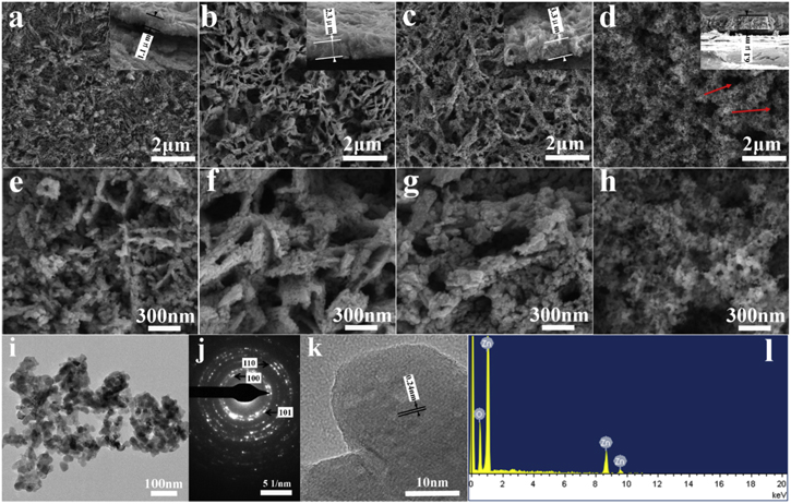
Figure 3. SEM images of Z120 (a) and (e), Z240 (b) and (f), Z360 (c) and (g) and P25 (d) and (h), insets (a)–(d) show the cross-sectional images. (i) is the TEM image of one nanosheet from Z240, (j) is the corresponding SAED pattern, and (k) is a HRTEM image from the above nanosheet. (l) is the EDS spectrum of Z240.
Download figure:
Standard image High-resolution image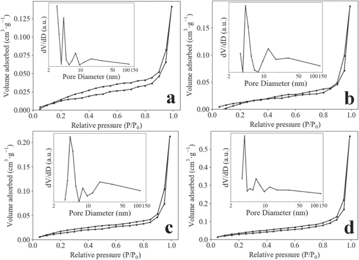
Figure 4. Nitrogen adsorption–desorption isotherms of Z120 (a), Z240 (b), Z360 (c) and P25 (d), insets is the responding pore size diameter plots.
Download figure:
Standard image High-resolution imageNitrogen adsorption–desorption measurements were used to further study the textural characteristics of the samples. The nitrogen adsorption–desorption isotherms of Z120, Z240, Z360 and P25 are drawn in figure 4. The isotherms of all the samples can be classified as Type IV due to the existence of hysteresis loops [40]. Moreover, the hysteresis loops are classified as Type H3 because they do not exhibit any unlimiting absorption at high p/p0. The SSA is evaluated by the following equation:

where SBET (m2) is the surface area estimated by Brunauer–Emmett–Teller equation, A (cm2) is the area of the sample for test, so SSA is unitless. By the equation (2), the SSA of Z120, Z240, Z360 and P25 are 104, 97.8, 97.1 and 174, respectively. The pore diameter distribution of Z120 (inset of figure 4(a)) reveals Z120 is a mesoporous structure with pore diameters mostly below 10 nm. Z240 and Z360 contain mesopores with diameters less than 10 nm and larger, as shown in insets in figures 4(b) and (c), where the strongest peaks locate at 4.3 nm for both Z240 and Z360, and the second strong peaks locate at 12.3 nm (Z240) and 17.3 nm (Z360), respectively. The pore size distribution of P25 (inset of figure 4(d)) is similar to that of Z120.
3.2. Optical properties
Diffuse reflectance spectroscopy (DRS) was used to evaluate the photon-capturing capability of the samples. The relative absorbance A = Log(1/R), where R is the relative reflectance, was taken as a measure for the absorption [41]. The UV–vis absorption spectra of Z120, Z240, Z360 and P25 are shown in figure 5(a). Z120, Z240, Z360 and P25 all exhibit typical absorption in the UV region. The UV-absorption edges of Z120, Z240 and Z360 is at about 380 nm, whereas the edge of P25 is at around 320 nm. The absorption ability of Z120, Z240, Z360 is significantly higher than that of P25 in the UVA (320–400 nm) and in the visible-light range. At 365 nm, which is used in the study of the photocatalytic activities, the absorbance of Z120, Z240, Z360 and P25 follows: A(Z240) ≈ A(360) > A(120) > A(P25). Generally, within a certain range, the UV absorption ability increases as the film thickness increases. The UV absorbance of Z240 is similar to that of Z360, proving that the UV absorption in Z240 has been saturated. In the visible-light range Z360 exhibits the best absorption ability, probably because it has the greatest thickness, and its nanosheets network provides the best geometrical conditions for multiple reflections and multiphoton absorption of visible light [42].
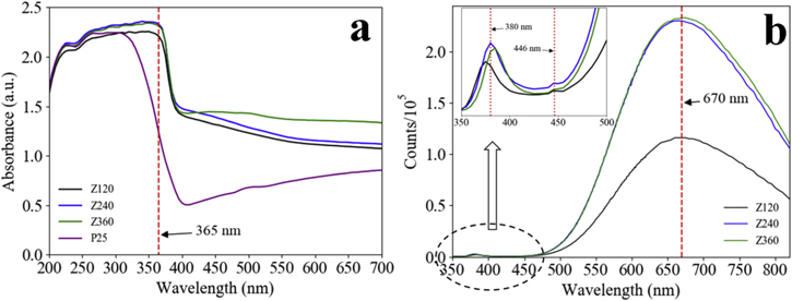
Figure 5. (a) UV–vis diffuse reflectance spectra of Z120, Z240, Z360 and P25. (b) PL spectra of Z120, Z240, Z360 in room temperature under excitation at 325 nm.
Download figure:
Standard image High-resolution imagePhotoluminescence (PL) spectroscopy was employed to probe bulk defects in the ZnO nanosheets. PL spectra of the ZnO nanosheets at room temperature under excitation at 325 nm are shown in figure 5(b). Z120, Z240 and Z360 all show three emission peaks, which are the broad and strong red emission peak centered at about 670 nm, the very weak ultraviolet emission peak centered at around 380 nm and the blue emission shoulder peak at 446 nm (inset). The peak at 380 nm is attributed to the near-band-edge excitonic transitions, which have been greatly suppressed. The red emission is attributed to oxygen vacancies (VO · ·) and oxygen interstitials (Oi '') in the boundary layer of crystalline grain [43]. The blue emission is probably related to zinc vacancies VZn [44]. The PL spectra are different from those of other reported ZnO for the ultraviolet emissions in the latter were stronger than or comparable to the visible emissions [45–48]. In the current case, the great disparity between the red emissions and ultraviolet emissions reveals that the ZnO nanosheets contain high content of VO · · and Oi '', and the content in Z240 is similar to that in Z360, but higher than that in Z120, because the latter has a lower ZnO coverage on the zinc substrate.
3.3. Photocatalytic activity
The photocatalytic activity of the samples was assessed by detecting the degradation of EA in air under UV irradiation with the same area of sample (21 cm2). Figure 6(a) shows the variation of the EA concentration with irradiation time with (and without) the samples as photocatalyst. In the absence of photocatalyst, EA undergoes slight photolysis with concentration dropping by 8.7 ppm in 120 min. The EA concentration is significantly reduced with Z120, Z240, Z360 and P25, and the photocatalytic degradation processes appears to follow the 1st order reaction kinetics. With Z120, the EA concentration drops from the initial 100.5 ppmto 40.2 ppm in 120 min, so EA has a removal percentage of 60.0%. The removal percentage with P25 is 78.1%, while the values with Z240 (86.0%) and Z360 (84.2%) are greater. The degradation byproducts with Z240 at 120 min were analyzed by GC-MS, and only CO2, water vapor and remaining EA were found.

Figure 6. Plots of the ethyl acetate concentration versus time with photocatalysts Z120, Z240, Z360, P25 or blank under ultraviolet irradiation (365 ± 5 nm, 24 mW cm−2). (b) Plots of ln(C/C0) versus irradiation time in presence of photocatalysts, where the slopes of fitted lines are the apparent 1st order reaction rate constants.
Download figure:
Standard image High-resolution imageApparent rate constant was used to evaluate the photocatalytic activity of the samples. Figure 6(b) shows the plots of ln(C/C0) versus time in above processes, where the slopes of the fitted lines are equal to the apparent rate constants of the 1st order reaction. The degradation rate (r) can be expressed by −r = kC, where k (min−1) is the apparent rate constant, C (ppm) is the concentration at any given time [49]. From figure 6(b), the k values of Z120, Z240, Z360, and P25 were found to be 0.0082, 0.017, 0.016 and 0.012 min−1, respectively.
The greater photocatalytic activity of P25 than Z120 should be ascribed to the positive effect of SSA, which not only increases the adsorption of EA but also provides more active sites [50, 51]. Z240 with smaller SSA exhibit greatest photocatalytic activity, which should be mainly attributed to its better UV absorption ability and higher content of VO · · and Oi ''. These defects can not only trap the photogenerated carriers to prevent recombination of excitons but also yield active sites, which can be expressed by reaction equations (3)–(5):


where  trap the photogenerated electrons temporarily to reduce the surface recombination of electrons and holes, and
  is a source of high effective oxidant ·OH; whereas Oi
'' acts as photogenerated holes' shallow trappers and provides ·OH through the redox reaction [52, 53].
is a source of high effective oxidant ·OH; whereas Oi
'' acts as photogenerated holes' shallow trappers and provides ·OH through the redox reaction [52, 53].
3.4. Performance in PEC water splitting
Figure 7(a) shows the LSV curves of Z120, Z240 and Z360 photoanodes in dark and under 100 mW cm−2 illumination. They all have low dark current densities due to good coverage of the zinc substrate. Moreover, the photocurrent densities increase significantly with the potential until saturations are reached at certain potentials (Z120 at −0.37 V, Z240 at −0.30 V and Z360 at 0.28 V). Such saturation behavior of photocurrent has been rarely observed for ZnO photoelectrodes. In the current case, it indicates the effective charge transfer in the ZnO nanosheets [54]. This can be explained by the fact that the boundary layer of the nanocrystallines in the nanosheets prohibited photogenerated electrons from transferring over it [43], facilitating the charge separation and collection. The saturated photocurrent densities of Z120, Z240 and Z360 are 0.13, 0.18 and 0.22 mA cm−2, respectively, comparable with those of most nanowires (nanorods) [4, 8, 54] and other porous ZnO [19, 21]. Figure 7(b) shows the current densities of Z120, Z240 and Z360 under chopped illumination at a fixed potential of 0 V (versus Ag/AgCl). They all exhibit rapid photoelectric responses, yet slight decline in the cycles (as highlighted by the dashed lines) due to the photocorrosion of the bare ZnO [55]. The photocorrosion of ZnO for photocatalysis application can be suppressed by crystal structure (morphology) design [56] or hybridization strategies [57]. The transient effect in power excitation [4] is also observed as the instantaneous photocurrent upon each illumination is relatively high.

Figure 7. (a) LSV curves of the Z120, Z240 and Z360 photoanodes in dark and under illumination of 100 mW cm−2. (b) Photocurrent densities versus time of the Z120, Z240 and Z360 photoanodes at 0 V versus Ag/AgCl under chopped illumination. (c) Mott–Schottky plots of the Z120, Z240 and Z360 photoanodes, measured with a 5 mV ac signal of 1 kHz and a step of 20 mV. (d) Nyquist plots measured at −0.8 V versus Ag/AgCl under illumination (100 mW cm−2), inset is the equivalent circuit model.
Download figure:
Standard image High-resolution image
The MS plots of the ZnO nanosheets are shown in figure 7(c). Z120, Z240 and Z360 photoanodes all show positive slopes, revealing they are n-type semiconductors. Moreover, Z360 has the minimum slope, corresponding to the greatest carrier density (Nd ) [58]. Flat-band potentials (VFB ) are determined by the intercepts of the linear portion of 1/C2 versus potential onto x-axis [58]. From figure 7(c), the VFB values of Z120, Z240 and Z360 photoanodes are −0.49, −0.31 and −0.30 V, respectively.
EIS were used to study the charge transport kinetics in the interface of sample/electrolyte under illumination. The Randles–Ershler equivalent circuit model is used [59], as shown in figure 7(d), in which Rs, Rct and CPE represent the electrolyte resistance, the charge transfer resistance and the constant phase element across the interface of sample/electrolyte, respectively. The Nyquist plots are shown in figure 7(d), in which the solid lines are fitted curves of the experimental data according to the equivalent circuit model. The fitted electronic parameters of the samples are shown in table 1, in which the Rct of Z360 (6558 Ω) is much smaller than those of Z120 (14342 Ω) and Z240 (9500 Ω), indicating Z360 provides a more favorable environment for reducing the recombination of photogenerated electron–hole pairs and for photogenerated holes transferring from the interface to the electrolyte [8].
Table 1. Fitted electronic parameters according to the equivalent circuit model in inset of figure 7(d).
| Photoanodes | Rs (Ω) | Rct (Ω) | CPE-T (F) | CPE-P |
|---|---|---|---|---|
| Z120 | 4.739 | 14 342 | 1.95 × 10⁻⁴ | 0.950 |
| Z240 | 4.298 | 9500 | 2.61 × 10⁻⁴ | 0.951 |
| Z360 | 4.263 | 6558 | 3.31 × 10⁻⁴ | 0.957 |
Z360 exhibites the highest photocurrent response can be explained by the visible light multiphoton absorption originated from the light reflection and trapping behavior [42]. When the nanosheets assemble into 3D network architectures, many gaps form between adjacent nanosheets. These gaps facilitate multiple reflections of the visible light which provide more interactions sites for light and ZnO. Furthermore, with the high content of native defects offering the mid-gap states which mediate the associated electronic transitions, the multiphoton absorption process occurs [60, 61]. The increase in the ZnO film thickness lead to deeper 'traps' and subsequent better light trapping and more visble light multiphoton absorption. As a result, Z360 with the greatest thickness possesses the best visble light absorption ability and the highest photocurrent response. However, a further increase in the film thickness is often accompanied by the stacking of the nanosheets, resulting in a decrease in visible light absorption ability [37].
4. Conclusion
In summary, porous ZnO nanosheets prepared by air cold plasma on zinc substrate showed good performance both in photocatalytic degradation and PEC water splitting. The ZnO nanosheets were rich in mesopores and consisted of nanocrystallines with high-density oxygen vacancies and oxygen interstitials in the boundary layers. The UV absorption tended to be saturated as the thickness increased, and the saturation occurred at a thickness of about 2.3 μm. The 2.3 μm thick sample with higher content of oxygen-related defects possessed the highest photocatalytic activity (and higher than P25 TiO2) in removal of gaseous ethyl acetate under UV irradiation. The ZnO nanosheets achieved a photocurrent density of 0.22 mA cm−2 (at −0.28 V versus Ag/AgCl) due to the excellent UV–vis absorption ability and the effective transfer of photogenerated carriers. The raw material of the ZnO nanosheets is only zinc foil with excellent mechanical flexibility, which enables large-scale industrial manufacturing of such ZnO photocatalyst.
Acknowledgments
This work was supported in part by the National Natural Science Foundation of China under Grant 60906053, Grant 61204069, Grant 61274118, Grant 61306144, Grant 61504079, and Grant 11605112, in part by the Scientific and Innovative Action Plan of Shanghai under Grant 15DZ1160800 and Grant17XD1702400, in part by the China Postdoctoral Science Foundation under Grant2016M601595.
Data availability statement
All data that support the findings of this study are included within the article (and any supplementary files).