

Abstract
The GeSn-based quantum wells (QWs) have been investigated recently for the development of efficient GeSn emitters. Although our previous study indicated that the direct bandgap well with type-I band alignment was achieved, the demonstrated QW still has insufficient carrier confinement. In this work, we report the systematic study of light emission from the Ge0.91Sn0.09/Ge0.85Sn0.15/Ge0.91Sn0.09 double QW structure. Two double QW samples, with the thicknesses of Ge0.85Sn0.15 well of 6 and 19 nm, were investigated. Band structure calculations revealed that both samples feature type-I band alignment. Compared with our previous study, by increasing the Sn composition in GeSn barrier and well, the QW layer featured increased energy separation between the indirect and direct bandgaps towards a better direct gap semiconductor. Moreover, the thicker well sample exhibited improved carrier confinement compared to the thinner well sample due to lowered first quantized energy level in the Γ valley. To identify the optical transition characteristics, photoluminescence (PL) study using three pump lasers with different penetration depths and photon energies was performed. The PL spectra confirmed the direct bandgap well feature and the improved carrier confinement, as significantly enhanced QW emission from the thicker well sample was observed.
Export citation and abstract BibTeX RIS
1. Introduction
Silicon-based light sources such as light emitting diodes (LEDs) and lasers have long been desired for optoelectronic integrated circuits [1, 2]. The recent development of group IV-based GeSn technique has opened a new avenue for photonic integration on the Si substrate [3–11]. The successful demonstration of GeSn LEDs and optically-pumped lasers using direct bandgap GeSn materials, indicates the great potential of GeSn for Si-based light sources [12–19]. In the last few years, GeSn LEDs with double heterostructures and quantum wells (QWs) have been reported [13–15, 20–36]. It is generally acknowledged that applying the QW structures to LEDs and lasers could improve their device performance, which motivated the investigation of GeSn LEDs based on the Ge/GeSn/Ge QW structure [30]. However, the detailed analysis suggested that using Ge as a barrier the QW featured type-II band alignment, and such structure could not provide direct bandgap of QW due to the relative large compressive strain of GeSn layer [32]. To achieve the direct bandgap well with type-I band alignment that can be practically used in efficient GeSn LED and laser devices, the relaxation of GeSn well is a critical issue as the compressive strain pushes the GeSn bandgap towards indirect [37, 38]. Therefore, the use of the GeSn and SiGeSn as the buffer as well as barrier were proposed, which could ease the compressive strain of GeSn well [1, 39]. The SiGeSn/GeSn and GeSn/GeSn QWs were grown and characterized recently [32, 35, 37, 38, 40]. By appropriately selecting the Si and Sn compositions, the SiGeSn and GeSn served as buffer and barrier layers. However, our previous study indicated that although direct bandgap well with type-I band alignment was achieved, the carrier confinement is still insufficient, which could reduce the QW light emission efficiency. Hence a QW structure featuring stronger carrier confinement is highly desirable.
To improve the carrier confinement, further relaxing the GeSn well to increase energy separation between its indirect and direct bandgap is a viable solution towards a better direct gap semiconductor. In this work, the Ge0.91Sn0.09 buffer layer was utilized, which features higher Sn composition compared to our previous work [40], and therefore could further relax the compressive strain of the GeSn well layer with Sn composition of 15%. Note that the 9%-Sn buffer layer could also serve as the barrier relative to the 15%-Sn well. As a result, the direct bandgap well with improved carrier confinement was obtained despite the residual compressive strain. Two GeSn/GeSn double QW samples, with different well thicknesses were grown and characterized. The temperature-dependent photoluminescence (PL) spectra were obtained and analyzed, which indicated that: (i) both samples feature improved carrier confinement by using higher Sn Ge0.91Sn0.09 buffer, as the temperatures of barrier emission disappearing were observed at 100 and 150 K, respectively, which are higher than previously reported QW of below 70 K [40]; (ii) the carrier confinement was further improved with thicker GeSn well sample, as evidenced by the temperature of barrier emission disappearing raises to 150 K, and the QW emission dominates the PL at lower temperature under 1064 nm pulsed laser pumping (barrier emission always dominates PL for thinner well sample and previous QW in [40]).
2. Experimental details
2.1. Material growth and characterization
Two QW samples (annotated as A and B) studied in this work were grown using an industry standard ASM Epsilon® 2000-Plus reduced pressure chemical vapor deposition system. Low-cost commercially available SiH4, GeH4, and SnCl4 were used as Si, Ge, and Sn precursors, respectively. The 700 nm-thick Ge buffer layer was grown prior to QW growth by a two-step growth method. The nominally designed QW structures consist of the followings from the bottom to top: (i) the 600 nm-thick Ge0.91Sn0.09 buffer for both samples A and B; (ii) two Ge0.85Sn0.15 wells (5 and 20 nm-thick for samples A and B, respectively) separated by a 2 nm-thick Ge0.91Sn0.09 barrier; and (iii) the Ge cap layer. For sample A, the well thickness of 5 nm features pseudomorphic growth to ensure the high material quality. While for sample B, the 20 nm thick well is partially relaxed, aiming to offer the improved carrier confinement. Material characterization (section 3.1) indicated that such partial relaxation did not deteriorate the material quality. To closely compare two QW samples, the 2 nm thick GeSn barrier designed for sample A (ensure the coupling between two wells) was also used for sample B. The detailed growth method has been described elsewhere [41].
After the growth, the secondary ion mass spectrometry (SIMS), high-resolution x-ray diffraction (HRXRD) 2θ-ω scan and reciprocal space map (RSM) were employed to identify and cross check the Sn compositions and the degree of strain of each layer. The bowing parameter of −0.066 was used for the lattice constant. The transmission electron microscopy (TEM) was used to examine the material quality and layer thickness, which were cross-checked by SIMS plots.
2.2. Band structure calculation
The band diagrams of the QW samples at 300 K were calculated using the measured QW structure data. The bowing parameters bΓ = 1.95 and bL = 0.68 were selected to determine the direct and indirect bandgap energies based on quadratic equation, which are valid for the high-Sn material [16, 32]. The effective mass approximation and the propagation matrix approach were used to calculate the electronic band structure and quantized energy levels [42]. The band offsets for conduction band (CB) and valence band (VB) were calculated by following the methods discussed in [8, 42].
2.3. PL study
The temperature-dependent PL measurements were performed using a standard off-axis configuration with a lock-in technique (optically chopped at 377 Hz). The emissions were collected using a spectrometer equipped with a thermoelectrically cooled PbS detector with cutoff at 3.0 μm. To pinpoint the optical transitions in QW, three lasers with various excitation conditions in terms of laser energy and beam penetration depth were utilized in this work: a 532 nm continuous wave (CW) laser, a 1550 nm CW laser, and a 1064 nm pulsed laser (pulse width of 5 ns and repetition rate of 45 kHz). The detailed parameters of pumping lasers are summarized in table 1.
Table 1. Parameters of pumping lasers.
| Laser wavelength (nm) | Laser spot diameter (μm) | Averaged power density (kW cm−2) | Photon injection density (photon number s−1 cm−2) | Penetration depth in GeSn (nm) |
|---|---|---|---|---|
| 532 | 65 | 15 | 4.1 × 10¹⁹ | 21 ± 2 |
| 1064 | 52 | 6a | 3.5 × 10²² | 418 ± 21 |
| 1550 | 24 | 160 | 1.2 × 10²¹ | 916 ± 46 |
aFor 1064 nm pulsed laser, the peak power density is 2.7 × 10⁴ kW cm−2.
The Gaussian fitting was used to investigate each peak in terms of peak position, full width at half maximum, and integrated PL intensity [40].
3. Results and discussion
3.1. Material characterization
The HRXRD 2θ-ω scans are shown in figures 1(a1) and (a2) for samples A and B, respectively. The black and red curves are the measured data and simulation results. In figure 1(a1), the peak at ∼66° indicates the Ge buffer. A small shoulder located at ∼66.5° is associated with the tensile strained Ge cap. The peaks at ∼65.0° and ∼64.2° correspond to GeSn buffer/barrier (measured as 8.8% Sn) and well (measured as 14.7% Sn), respectively. The multiple oscillations are associated with the thickness of the multi-layered structure (thickness fringes). Their presence indicates the high quality of the layer interfaces. The XRD 2θ-ω simulation was conducted to further analyze the QW, by which the lattice constant and layer thickness can be determined. The RSM shown in figure 1(a1) inset shows the clear three regions. The bottom region corresponds to the superposition of Ge buffer and cap layers. The region above the Ge indicates the contour plot of the almost relaxed Ge0.91Sn0.09 buffer/barrier with the residual compressive strain of 0.14%. The top region is the Ge0.85Sn0.15 well that is pseudomorphic to the relaxed Ge0.91Sn0.09 buffer.
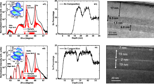
Figure 1. (a1), (a2) HRXRD 2θ-ω scan of samples A and B. The black and red curves are measured data and simulation results, respectively. Inset: the RSM contour plot; (b1), (b2) SIMS of samples A and B showing the Sn composition in each layer; (c1), (c2) TEM images of samples A and B.
Download figure:
Standard image High-resolution imageFigure 1(a2) shows the XRD results of sample B. The similar 2θ-ω scan and RSM plot were obtained except the following: (i) since the measured Sn compositions in GeSn buffer/barrier (9.4%) and well (15.3%) of sample B are higher than those of sample A, the GeSn peaks in 2θ-ω scan exhibit at ∼64.8° and 63.9°, shifting towards lower angle as expected; (ii) due to the thicker well of sample B (close to the critical thickness), the layer is partially relaxed, as shown in figure 1(a2) inset.
Figures 1(b1) and (b2) show the SIMS plots of samples A and B, respectively. It can be seen that the Sn composition in each layer is uniform. Although the transition at each interface is not very abrupt, the GeSn buffer, well, barrier and Ge cap regions can be clearly resolved.
Figures 1(c1) and (c2) show the cross-sectional TEM images of the QW samples. For both samples, each layer can be clearly resolved. The smooth cross section profile indicates the very low defect density. Particularly, for sample B, even though the Ge0.85Sn0.15 well layers feature partial relaxation, there are almost no threading dislocations propagating across the QW, resulting in high material quality. The measured thickness of each layer from TEM images is consistent with the value that was extracted from the simulated XRD 2θ-ω scan curve. On the other hand, compared to the design, the thicknesses of GeSn wells and barriers, and Ge caps show very close values for both samples A and B. Such small thickness variation would not affect the QW characteristics in this work. Material characterization results are summarized in table 2.
Table 2. Information of GeSn QW samples.
| Sn (%) | Thickness (nm) | |||||
|---|---|---|---|---|---|---|
| Samples | Layer structure | Designed | Measured | Designed | Measured | Strain (%) |
| A | Ge cap (top barrier) | 0 | 0 | 17.0 | 17.0 | 0.9 |
| GeSn well | 15 | 14.7 | 5.0 | 6.5 | −1.05* | |
| GeSn barrier | 10 | 8.8 | 2.0 | 1.5 | −0.26* | |
| GeSn well | 15 | 14.7 | 5.0 | 6.0 | −1.05* | |
| GeSn buffer (bottom barrier) | 10 | 8.8 | 600 | 600 | −0.14* | |
| Ge buffer | 0 | 0 | 700 | 700 | 0.2 | |
| B | Ge cap (top barrier) | 0 | 0 | 7.0 | 7.0 | 1.15 |
| GeSn well | 15 | 15.3 | 20.0 | 19.0 | −0.91* | |
| GeSn barrier | 10 | 9.4 | 2.0 | 2.0 | −0.11* | |
| GeSn well | 15 | 15.3 | 20.0 | 19.0 | −0.91* | |
| GeSn buffer (bottom barrier) | 10 | 9.4 | 600 | 600 | −0.11* | |
| Ge buffer | 0 | 0 | 700 | 700 | 0.21 | |
*Negative value indicates the compress strain.
3.2. Band structure and optical transition analysis
The band diagram of the QW samples at 300 K were calculated using the measured QW structure data shown in table 2. Figures 2(a)–(d) illustrate the band structures at CB and VB and possible optical transitions of sample A. Using selected bowing parameters bΓ = 1.95 and bL = 0.68, and considering the compressive strain of −1.05%, the direct bandgap Ge0.853Sn0.147 well was obtained with the energy difference between Γ–L valley of 26 meV. Due to quantized energy levels in the well, the first energy levels in CB (n1Γ) and VB (n1HH) were calculated as 24 meV above the Γ valley minimum and 15 meV below the heavy hole (HH) band maximum, respectively. Figure 2 shows the barrier heights at each layer interface, which revealed that the type-I band alignment was achieved. In figure 2(a), in the CB, the barrier height between GeSn barriers (including bottom barrier and inter-barrier) and GeSn well was calculated as 17 meV; while the barrier height at GeSn well/Ge top barrier interface is 93 meV. In the VB, the residual strain results in the split of HH and light hole (LH) bands. The barrier heights at GeSn barrier/GeSn well and GeSn well/Ge barrier interfaces are 54 and 160 meV, respectively. In figure 2(d), the barrier heights between GeSn barrier and GeSn well at L-valley and LH band are less than 5 meV; while at the GeSn well/Ge barrier interface, the barrier heights were calculated as 33 and 49 meV at L-valley and LH band, respectively.
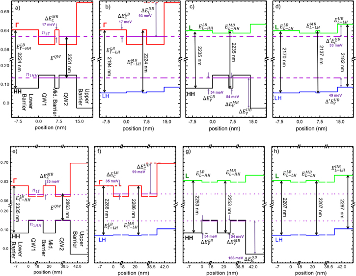
Figure 2. Top: for sample A. Band diagram calculated based on measured material data, showing the carrier confinement and the possible band-to-band optical transitions between (a) Γ–HH; (b) Γ–LH; (c) L–HH; and (d) L–LH. (Unit: meV). Bottom: for sample B. (e)-(h) The similar band diagram and optical transition calculations.
Download figure:
Standard image High-resolution imageSince the 17 meV (0.66 kBT) barrier height between GeSn barriers and GeSn well in the Γ valley does not provide surfficient electron confinement, the electrons at n1Γ could gain thermal energy and populate the Γ valleys in the GeSn barrier layers at room temperature. In addition, the first quantized energy level in L valley is only a few meV above n1Γ in GeSn well, the electrons could also be thermally excited to populate the L valley, followed by populating the L valleys in the GeSn barriers due to weak carrier confinement. The re-distributed electrons leading to the recombinations could occur between different energy bands (including L valley to VB with phonon assistance) in multiple layers, resulting in the optical transitions being originated from multiple recombination mechanisms. Figures 2 (a)–(d) illustrate the possible transitions.
Figures 2(e)–(h) illustrate the band structures and possible optical transitions of sample B. The energy separation between Γ–L valley of direct bandgap Ge0.847Sn0.153 well was calculated as 52 meV, which is higher than that of sample A due to the higher Sn composition. It is worth noting that the Ge0.906Sn0.094 barrier also features direct bandgap, as the Γ valley is 19 meV below the L valley. In figure 2(e), in the CB, the barrier heights at GeSn barrier/GeSn well and GeSn well/Ge barrier interfaces were calculated as 35 and 99 meV in Γ valley, respectively; while in the VB the barrier heights are 54 and 166 meV at HH band, respectively. The improved electron confinement in Γ valley and HH band compard to sample A is mainly due to the higher Sn composition and thicker GeSn well layer of sample B. The barrier heights in L valley and LH band are less than 5 meV between GeSn barriers and well, as shown in figures 2(f) and (g).
It is worth noting that for samples A and B, there are several quantized states for electrons and holes in wells. The transitions from higher order quantized states could also contribute to QW emission, which, however, is very difficult to be further identified due to small energy difference.
Although the improved barrier height between GeSn barriers and GeSn well in the Γ valley of 35 meV (1.35 kBT) at room temperature, some electrons at n1Γ could be thermally excited to populate the Γ valley in the GeSn barrier layers, leading to the multiple recombination mechanism including direct transition from well, and direct and indirect transitions from barrier. Moreover, since there is almost no carrier confinement in L valley and LH band between GeSn barrier and well, the carrier could flow from one to the other, resulting in the phonon assisted optical transitions that could occur in both layers. The detailed transition mechanism is discussed in the following section via the PL spectra analysis.
3.3. PL spectra analysis
Figure 3(a) shows the normalized temperature-dependent PL spectra of sample A using a 532 nm CW laser. The spectra were stacked for clarity. At 300 K, a major higher energy peak at 2220 nm (0.558 eV) and a small lower energy shoulder at 2560 nm (0.484 eV) were observed. As the temperature decreases, both peaks shift towards shorter wavelength. For the higher energy peak, the peak intensity decreases as the temperature decreases. At temperatures below 100 K, the higher energy peak almost disappears; while for the lower energy peak, the intensity increases significantly as the temperature decreases. This lower energy peak was assigned to the QW emission as the emission energy of 0.484 eV at 300 K is consistent with the calculated value of 0.486 eV shown in figure 2(a). At 10 K, the integrated PL intensity is over 100 times higher than that at 300 K, as shown in figure 5(a). The significantly increased PL intensity at lower temperature clearly indicates the direct bandgap material nature, matching well with band structure calculation. The higher energy peak was mainly attributed to Γ–HH transitions at GeSn barriers since the transition energy (0.558 eV) is very close to calculated one (0.557 eV). However, due to the thermally re-distributed carriers, the Γ–LH (0.565 eV) and L–HH (0.555 eV) transitions at GeSn barriers, and L–LH transition (0.568 eV) at Ge barrier could also contribute to the PL, i.e., the higher energy peak might consist of multiple peaks with partial overlap. These peaks cannot be further identified due to their small energy separation. Note that at 300 K the multi-peak feature at ∼2700 nm is due to the CO2 absorption peak, which disappears at lower temperature due to peak blue-shift. Such peak does not affect the PL spctra analysis.
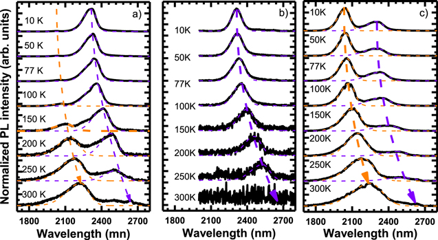
Figure 3. Temperature-dependent PL spectra of the sample A using (a) 532 nm CW laser; (b) 1550 nm CW laser; and (c) 1064 nm pulse laser. The multi-peak feature at ∼2700 nm is due to CO2 absorption. The dashed lines are eye guidance of peak shift.
Download figure:
Standard image High-resolution imageIt is worth noting that our previous QW study showed that the GeSn barrier emission almost disappears below 70 K [40]; while in this work, under the same pumping condition, the temperature of barrier emission disappearing raises to 100 K. This revealed that by using higher Sn buffer, the significant reducing of thermal activated carriers occurs at higher temperature compared to our previous QW, indicating the improved carrier confinement.
Since the penetration depth of the 532 nm laser is only ∼21 nm, the major absorption occurs only in the Ge top barrier and the QW and barrier emission are due to the carrier redistribution. To further analyze the optical transitions, a 1550 nm CW laser and a 1064 nm pulsed laser were used as pumping sources, which feature more than 400 nm penetration depth (see table 1), and therefore each layer could be involved in light absorption. Figure 3(b) shows the normalized temperature-dependent PL spectra of sample A using a 1550 nm CW laser. At 300 K, the peak feature is unclear due to lower signal-to-noise ratio because of lower light absorption under 1550 nm pumping than that under 532 nm pumping. Below 250 K, a single peak at each temperature was observed. The temperature-dependent peak position and shift are very similar to the lower energy peak shown in figure 3(a), indicating that this peak is due to the QW emission. As can be seen in figure 5(a), the integrated PL intensity increases 40 times from 250 to 10 K. Note that the emission from any other transitions was not observed under 1550 nm laser, which can be interpreted as follows: the increased penetration depth of 1550 nm laser beam enhances the light absorption in the GeSn barriers. At lower temperature, the photo-generated carriers would flow into the GeSn well region due to the improved carrier confinement because of reduced thermal energy kBT, which minimizes the emission from barrier and consequently leads to enhanced QW emission.
Figure 3(c) shows the normalized temperature-dependent PL spectra of sample A using a 1064 nm pulse laser. At each temperature, two clear peaks were obtained. The peak position and shift as temperature decreases are very close to those under 532 nm laser pumping, indicating that the higher and lower energy peaks are attributed to transition from barriers and well, respectively. Note that the peak intensity from barriers is always higher than that from well. This is due to the high injection level (see table 1) under the pulsed pumping by the 1064 nm laser and its deep penetration depth, a huge number of photo-generated carriers populates the GeSn well, GeSn and Ge barriers simultaneously. Electron–hole recombination in GeSn and Ge barriers could occur before the carriers re-distribute to the GeSn well via the carrier confinement effect, resulting in the PL spectra consisting of emissions from barriers and well with more pronounced contribution from GeSn and Ge barrier layers. Moreover, in figure 5(a) it can be seen that the integrated PL intensity of barriers emission increases 2.2 times as the temperature decreases from 300 to 10 K, while the well emission increases 8.6 times. This can be explained as the better carrier confinement at low temperature due to reduced kBT which enhances the QW emission.
The normalized temperature-dependent PL spectra of sample B using 532 nm CW, 1550 nm CW, and 1064 nm pulse lasers are shown in figures 4(a)–(c), respectively. In figure 4(a), at 300 K, a clear peak at 2330 nm (0.532 eV) and a weak-signal peak at ∼2800 nm (0.443 eV) were observed. As temperature decreases, both peaks exhibit blue-shift as expected. The higher energy peak features reduced intensity and disappears below 150 K; while the lower energy peak shows dramatically increased intensity, as the integrated PL intensity at 10 K is over 450 times higher than that at 300 K as shown in figure 5(b), indicating the direct bandgap material nature. The lower energy peak is assigned to QW emission. Compared to the calculated value of transition energy (0.433 eV), the deviation of 0.01 eV is mainly from the error of Gaussian fitting due to the weak peak intensity. The higher energy peak is mainly attributed to Γ–HH transitions at GeSn barrier as the transition energy (0.532 eV) matches well with calculated value of 0.531 eV. However, the broadened peak line-width suggests that other transitions could contribute to the PL as well, including Γ–LH (0.542 eV) and L–HH (0.550 eV) transitions at GeSn barriers, and L–LH (0.562 eV) Γ–LH transition (0.547 eV) at Ge barrier. Note that the temperature of barrier emission disappearing of sample B is 150 K, which is higher than that of sample A (100 K) and our previously reported QW (70 K, [40]). This implies that: (i) by using high Sn buffer, both samples A and B feature improved carrier confinement compared to previous reported QW; (ii) compared to sample A, sample B exhibits further improved carrier confinement by using thicker GeSn well that further ease the compressive strain. The experimental evidence confirms the band structure calculation results shown in figure 2.
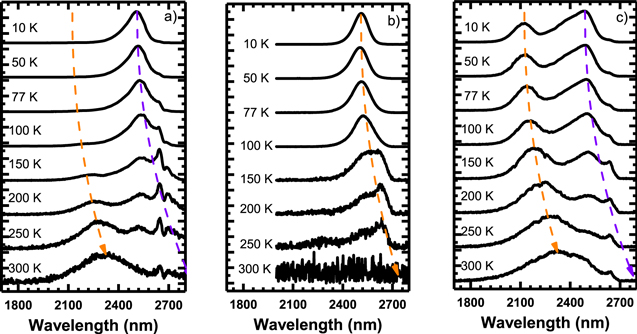
Figure 4. Temperature-dependent PL spectra of the sample B using (a) 532 nm CW laser; (b) 1550 nm CW laser; and (c) 1064 nm pulse laser. The feature at ∼2700 nm is due to CO2 absorption. The dashed lines are eye guidance of peak shift.
Download figure:
Standard image High-resolution image
Figure 5. Integrated PL intensity of (a) sample A; and (b) sample B.
Download figure:
Standard image High-resolution image
Figure 4(b) shows the normalized temperature-dependent PL spectra of sample B using a 1550 nm CW laser. The similar single peak feature as sample A was obtained. Based on the peak energy and shift trend, this peak is assigned to QW emission. The broadened peak line-width at 250, 200, and 150 K is mainly due to the partial overlay of emissions from QW and defects. Below 150 K, the dramatically increased intensity of QW peak leads to non-observable defect peak. As shown in figure 5(b), the integrated PL intensity increases 150 times from 250 to 10 K.
Figure 4(c) shows the normalized temperature-dependent PL spectra of sample B using a 1064 nm pulse laser. At 300 K, the intensity of GeSn barrier peak is higher than that of GeSn well. As temperature decreases, since the GeSn barrier and well are both direct bandgap material according to band structure calculation, both peak intensities increase with more rapid growth of QW peak than the barrier peak. Below 100 K, the emission from GeSn well is stronger than that from GeSn barriers. At 10 K, the integrated PL intensities increase 16 and 3 times for well and barrier, respectively, as show in figure 5(b). The strong QW emission can be explained as following: since the QW structure of sample B provides sufficient carrier confinement at lower temperature, most photo-generated carriers eventually tend to populate the Γ valleys in GeSn well, resulting in that majority emissions are from band-to-band transitions in well. However, due to the high injection level, some electron–hole pairs could recombine before flowing into the well region, leading to the emissions from Ge and GeSn barriers.
It is worth noting that under 1064 nm laser pumping, compared to sample A, the sample B exhibits dramatically enhanced emission from QW, as QW peak dominates the PL below 100 K (for sample A, the barrier emission always dominates the PL). This is mainly due to the thicker GeSn well of sample B further relaxes the material, and consequently lowers the first quantized energy level in well, resulting in improved carrier confinement compared to sample A.
4. Conclusion
In conclusion, two GeSn/GeSn double QW samples with different well thicknesses were grown and analyzed in depth. By using relaxed GeSn buffer with higher Sn composition, improved carrier confinement was achieved, which was revealed by band structure calculation and confirmed by temperature-dependent PL spectra. At 300 K, the QW emission peaks at 2560 nm and 2800 nm for samples A and B were observed, respectively. The peak intensity increased dramatically as temperature decreased to 10 K, indicating a typical direct bandgap behavior. The transitions from Ge and GeSn barriers were also obtained and the peaks are partially overlapped due to small energy separation. Comparing samples B to A, the higher Sn composition in well and increased well layer thickness lead to the increased energy separation between the direct and indirect bandgap and significantly enhanced carrier confinement of sample B. Particularly at lower temperature, the sufficient carrier confinement of sample B results in hundreds times integrated PL intensity increase under CW pump lasers, and the QW emissions dominating the PL under both CW and pulse pump lasers. Guided by the results provided in the work, more efforts would be made to optimize the QW structure such as well thickness to further improve the carrier confinement as well as discreteness of quantized state, towards the demonstration of room temperature operation devices such as lasers.
Acknowledgments
The work was supported by Air Force Office of Scientific Research (AFOSR) (FA9550-16-C-0016 and FA9550-14-1-0205) and the National Science Foundation (NSF) (DMR-1149605). The authors would like to thank Dr Mourad Benamara for his help on using high-resolution TEM at the Institute for Nanoscience and Engineering, University of Arkansas.