
Abstract
Nanosecond pulsed two-beam laser interference is used to generate two-dimensional temperature patterns on a magnetic thin film sample. We show that the original domain structure of a [Co/Pd] multilayer thin film changes drastically upon exceeding the Curie temperature by thermal demagnetization. At even higher temperatures the multilayer system is irreversibly changed. In this area no out-of-plane magnetization can be found before and after a subsequent ac-demagnetization. These findings are supported by numerical simulations using the Landau–Lifshitz–Bloch formalism which shows the importance of defect sites and anisotropy changes to model the experiments. Thus, a one-dimensional temperature pattern can be transferred into a magnetic stripe pattern. In this way one can produce magnetic nanowire arrays with lateral dimensions of the order of 100 nm. Typical patterned areas are in the range of several square millimeters. Hence, the parallel direct laser interference patterning method of magnetic thin films is an attractive alternative to the conventional serial electron beam writing of magnetic nanostructures.
Export citation and abstract BibTeX RIS

Content from this work may be used under the terms of the Creative Commons Attribution 3.0 licence. Any further distribution of this work must maintain attribution to the author(s) and the title of the work, journal citation and DOI.
1. Introduction
Tailoring magnetic properties on a nanometer length scale is a necessary ingredient for most spintronic devices (e.g. magnetic random access memories or sensors). These structures are generally fabricated by lithographic techniques like electron beam lithography which include the use of a photoresist, the serial development of the resist by the electron beam, the removal of the developed resist and an etching process e.g. by ions. In contrast, direct laser interference patterning (DLIP) which we implement here is (i) a one step production process which does not need any photoresist processing [1] and (ii) a parallel process which allows the processing of square millimeter samples with a single shot. Furthermore, by changing the wavelength and the intensity it can be adapted to different materials ranging from metals [2, 3] to polymers [4, 5]. Here, we focus on the application of DLIP on [Co/Pd] multilayer thin films which show a perpendicular magnetic anisotropy [6, 7].
The magnetic properties of [Co/Pd] multilayers depend on the interfaces of the separate layers [8–10]. It has already been demonstrated that a controlled modification of the multilayer interfaces with a laser beam leads to a change in anisotropy [11]. Here, we study the effect of DLIP laterally resolved on the magnetic structure directly after the laser pulse as well as after a demagnetization routine using a damped ac-magnetic field (further referred to as ac-demagnetization).
We observe thermal demagnetization in the experiment using a nanosecond laser, an effect which is frequently observed in ultrafast demagnetization processes with fs-lasers [12]. Here we focus on the characteristic changes in the magnetic domain pattern and how—for higher peak temperatures—the material properties themselves are influenced and can be controlled on a nanometer length scale. Our experimental investigation is supported by numerical simulations using the Landau–Lifshitz–Bloch (LLB) formalism for micromagnetics at elevated temperatures [13].
2. Methods
2.1. Direct laser interference patterning
DLIP is based on the interference of multiple beams, allowing the creation of an intensity and thus a temperature pattern on a surface [1, 14, 15]. This pattern depends on the number of interfering beams and their respective incident angles, their polarization and their intensities. The resulting maximum temperature depends additionally on the reflectivity, the absorption, the heat conductivity of the sample and the laser pulse length.
For the studies shown here, we will only discuss two interfering beams which lead to an intensity pattern given by a  -distribution. The period d of the pattern can be varied by the incident angle θ normal to the surface, where
  with the wavelength of the laser pulse λ. In our setup we used the second harmonic of an injection seeded Nd:YAG laser pulse (
 nm) with a pulse width of 12 ns. The achievable periodicities in our experiment are between 300 nm and 300 μm. Figure 1(a) shows the experimental setup which consists of a 50:50 beam splitter, two mirrors and a combination of a
  -wave plate with a Glan–Taylor polarizer in order to adjust the laser power continuously. The calculated intensity distribution, which is a convolution of the nearly Gaussian intensity distribution of the laser pulse (diameter 8 mm) and the
  -distribution resulting from the two-beam interference is depicted in figure 1(b).
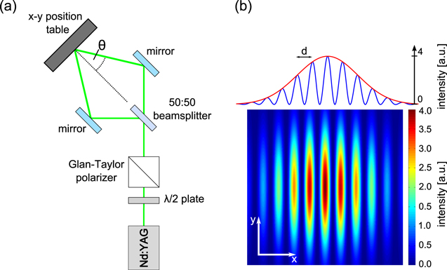
Figure 1. Schematic experimental two-beam interference setup (a) with the calculated lateral intensity distribution of a two beam interference pattern with a line profile (b).
Download figure:
Standard image High-resolution image2.2. Magnetic imaging
Magnetic force microscopy (MFM) is used to probe the magnetic domain structure of our samples. For that purpose, a Bruker MultiMode atomic force microscope with a high resolution magnetic probe of TeamNanotec (HR-MFM-ML3) is used to scan across the surface and in the lift-mode at a distance between 30 to 60 nm above the sample, where the magnetic force is dominant. In order to study the demagnetized domain configuration of our material, ac-demagnetization with a peak amplitude of 2 T is used prior to the MFM measurements.
2.3. Sample preparation
The [Co/Pd] multilayer thin films were sputter deposited onto Si(100) substrates with a native oxide layer. A background pressure of Ar was adjusted to  mbar for all depositions, while the base pressure of the deposition chamber was
  mbar. During the depositions the thickness was monitored using a quartz micro balance, which was calibrated by x-ray reflectometry measurements on Co and Pd thin film samples. Here, we study multilayer systems consisting of (Co(0.28)/Pd(0.9 nm))8 with 3 nm Ta and Pd seed layers and a 1.1 nm thick Pd capping layer to prevent oxidation. A schematic of the [Co/Pd] multilayer structure with a strong perpendicular anisotropy measured by Kerr magnetometry is shown in figure 2 as well as the ac-demagnetized domain distribution.
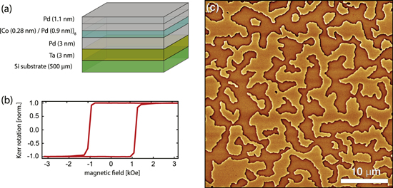
Figure 2. Detailed stack structure of the [Co/Pd] multilayer thin film (a) showing a strong out of plane anisotropy in the Kerr measurement (b) and the ac-demagnetized domain structure shown in the MFM image (c).
Download figure:
Standard image High-resolution image2.4. Theoretical model
In our corresponding simulations, a multiscale model is used describing the dynamics of the thermally averaged reduced magnetization  via the stochastic LLB equation [16, 17]. It is well established for instance in the context of spin-caloritronics [18, 19], or ultrafast magnetization dynamics [20, 21]. The advantage of using this thermal multi-macrospin approach as compared to atomistic spin model simulations is the possibility of simulating much larger system sizes and longer time scales. Contrary to conventional micromagnetic simulations based on the Landau–Lifshitz–Gilbert (LLG) equation of motion, the length of the magnetization vector is not conserved, it rather allows for longitudinal fluctuations of the magnetization in space and time and all relevant magnetic material parameters such as exchange stiffness, parallel and perpendicular susceptibilities, and equilibrium magnetization become functions of temperature that are well-defined in terms of their microscopic degrees of freedom. These equilibrium functions have been calculated in [13] for FePt based on atomistic spin model simulations. For the current work we rescaled these functions to match the material properties of a [Co/Pd] multilayer system [22, 23]. The corresponding zero-temperature material parameters are a saturation magnetization of
  , an exchange stiffness
  and an anisotropy constant
  , where we have used the relation
  . The LLB equation in the stochastic form reads
Besides the usual precession and relaxation terms of the LLG equation, the LLB equation contains another term which controls longitudinal relaxation. For  the temperature dependent longitudinal and transverse damping parameters,
  and
and  , are connected to the atomistic damping parameter λ via
  and
and  , with the Curie temperature
  . The additive fields
  and
and  representing the thermal fluctuations have the properties of white noise [17]. The effective fields
  are given by [24]
Here, the first term represents the anisotropy field which makes the z axis the easy axis of the model. The second term is the exchange field where  is the zero-temperature saturation magnetization and Δ is the cell size of the mesh. The numerical methods are described in detail in [24].
3. Results and discussion
In order to investigate the effects of annealing using laser interference patterning on [Co/Pd] multilayers on small periods, it is useful to start with a large patterning period as the effects are laterally stretched. Therefore, we use a 55 μm period before we investigate periods in the sub-micron range later on.
Figure 3 shows the topography and the magnetic structure after a single interference shot and we observe different regions which can be clearly distinguished. Most of the sample surface is unchanged and only in the center of the intensity maximum the topography shows variations of around a 100 nm (see figure 3(a)). The resulting surface structure in region III arises from a combination of dewetting of the metal film and substrate damage.
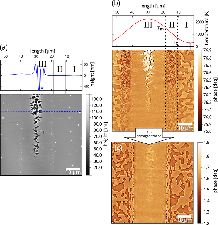
Figure 3. (a) AFM image of a [Co/Pd] multilayer thin film after a temperature pattern with a 55 μm period with the appropriate height profile. (b) MFM image of the magnetic structure after the temperature pattern showing three regions with different domain sizes. The temperature profile is calculated using the patterning period, the melting temperature  and the room temperature
  . (c) MFM image of the identical region after a subsequent ac-demagnetization step.
Download figure:
Standard image High-resolution imageIn contrast to the topographic changes, the magnetic structure shows three different regions (see figure 3(b)). In region I the domain size remains unchanged in the ac-demagnetized state. Towards higher intensities, and thus higher temperatures, an abrupt change in domain size can be observed (region II). There, the domain size is distinctively smaller which is also known as thermal demagnetization in the field of all-optical switching [25–27]. At even higher temperatures a second transition sets in with no detectable out-of-plane magnetic contrast anymore. The strong phase signal in the center of region III is only an artifact due to a cross-link between the height information and the phase signal and will be neglected in the discussion.
In order to quantify this temperature-dependent magnetic behavior assumptions on the temperatures have to be made. Earlier measurements showed that the out-of-plane magnetization disappears upon melting due to a steep increase of diffusion in the liquid phase [6]. Thus, we assume that the transition from region II to region III is connected to the typical melting temperature of [Co/Pd] multilayers  K [28]. If we suppose further that in the intensity minima the sample is still at room temperature and that the temperature of a metal thin film increases in first order linearly with the absorbed intensity, we can deduce the threshold temperature of region II. The resulting temperature distribution is shown in figure 3(b) and we determine a temperature of around
  . In order to measure
  in our multilayer system, temperature-dependent saturation magnetization measurements using a superconducting quantum interference device magnetometer have been carried out (not shown here). A fit towards higher temperatures leads to
  which agrees very well with the experimental finding of the threshold temperature of region II.
We study this transition now with the help of supporting simulations. In general the domain configuration of a thin magnetic film is generated by a competition between short-ranged exchange and anisotropic interaction and the long-ranged dipole–dipole interaction. Therefore, the resulting average domain size highly depends on the shape of the sample (geometry, thickness, width) as well as on the strength of the temperature-dependent material parameters as magnetization, exchange and anisotropy. For films with perpendicular anisotropy such as in our case this relation can be described by the so-called quality factor Q given by the ratio of total anisotropic to stray field energy [29], where  leads to an in-plane magnetization, while
  results in an out-of plane magnetization. Additionally, in realistic systems the influence of local defects pinning magnetic domain walls in local energetic minima can play a crucial role for the resulting magnetic configuration. In our simulations this effect is considered by including a certain percentage of randomly distributed holes (cells without magnetization) into the sample.
In order to explain the experimental findings, we have modeled a thin film with the size of 1024 nm × 1024 nm × 16 nm discretized with a cell size of 4 nm. For a proper discretization the cell size has to be smaller than the domain wall width of the material given by  [30]. Therefore even with the usage of our multi macrospin model we are still limited to much smaller system sizes and shorter timescales in comparison to the experiment. Therefore, in our simulations we focus firstly only on a single hot line of the laser pattern and secondly only on the stability conditions of the domain structure after cooling. The stable starting configuration for 300 K as shown in the left column of figure 4 has been generated by slowly cooling down the sample from the paramagnetic phase. We note that also simulations with ac-demagnetization similar to the experiment have resulted in equivalent domain structures.
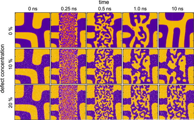
Figure 4. Simulated results for the temporal development of the magnetic configuration of one hot line for different defect concentrations ( ). Here, the color coding for the reduced out-of-plane magnetization goes from yellow (up) over red (zero) to purple (down), with defects plotted in white.
Download figure:
Standard image High-resolution imageStarting with this configuration, we have modeled the laser heating with its subsequent cooling process for different defect concentrations by assuming the following spatial and temporal temperature profile
where the maximal temperature increase as well as the temporal and spatial maximum shift and the characteristic relaxation constants have been set to  ,
,  ,
,  ,
,  and
and  . The resulting domain configurations for different times are shown in figure 4. For the case without any defects, as plotted in the first row, in the central area the maximal temperature has exceeded the Curie temperature and directly after cooling down from the paramagnetic to the ferromagnetic phase (0.25 ns) very small domains are building up. The size of these domains increases then with time until approximately after 10 ns a state equivalent to the starting configuration is reached again. By including defects in the system, this domain growth is stopped after a certain time, since the smaller domains remain pinned at local energetic minima. With increasing defect concentration this pinning effect becomes more pronounced, leading to a faster stabilization of domain configurations with much smaller domain sizes. This tendency of an increasing number of defects leading to smaller stable domains in the central area of the film where
  was above
  is shown in the right column of figure 4.
This theoretical result agrees very well with the experimental findings as plotted in figure 3, where the abrupt transition between small domains in the area where the temperature has reached the Curie point (region II) and much larger domains in the area of lower laser intensity (region I) is obtained.
Another effect taking place during the thermal demagnetization process of the sample is the decrease of anisotropy. Within our modelling this has been investigated by assuming a reduction of anisotropy constant following the laser pulse. This was taken into account assuming the following spatial profile for the relative reduction of the anisotropy constant

where we have used  nm and
  nm for the maximum shift to the center and the relaxation constant, respectively. In order to separate both effects, this time we have not assumed any defects in the system. The corresponding results for the temporal development of the magnetic structure with
  and
and  are shown in figure 5.

Figure 5. Simulated results for the temporal development of the magnetic configuration of one hot line for several anisotropy reductions ( ).
).
Download figure:
Standard image High-resolution imageBy reducing the anisotropy in the center to 50  of its original value (first row), the magnetization still remains oriented out-of-plane (
 ), but a stable configuration with smaller domains in the center is reached. For even higher reductions of the anisotropy (second row) the quality factor Q becomes smaller than 1 leading to a switching from the out-of-plane to the in-plane direction in this area.
Compared to the experimental results shown in figure 3, we expect a combination of these two effects. In figure 6 we show the temporal development of the magnetic domain configuration of a system with 20% defects as well as a 65% anisotropy reduction ( K,
K,  ps,
ps,  ps,
ps,  nm,
nm,  nm,
nm,  and
and  nm). We obtain that the irreversible change of the anisotropy corresponds to the out-of-plane region III of figure 3, whereas the small domains in region II are mainly caused by the reversible pinning effect.

Figure 6. Simulated results for the temporal development of the magnetic configuration of one hot line for a combination of a reduced anisotropy ( ) and included defects (
 ).
).
Download figure:
Standard image High-resolution imageIn the experiment of figure 3 after ac-demagnetizing the sample shows a narrow region with a changed domain size at the transition between region II and III, whereas most of the previous small domains are restored in the original state (see figure 3(c)). We note that the transition between region II and III can also be explained by the irreversible anisotropy change in the sample, where contrary to region III the quality factor Q has remained above 1 leading to smaller out-of-plane domains (see second row in figure 5). Thus, the sample consists mainly of stripes with the original domains and stripes with no out-of-plane magnetization.
This model holds also for the small periods. The two types of different magnetic regions are also obtained, as it is shown in figure 7 for samples which were illuminated with interference periods of 1 μm (figure 7(a)) and 650 nm (figure 7(b)) and subsequently ac-demagnetized.
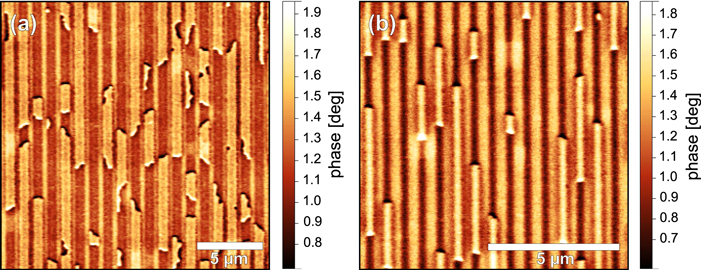
Figure 7. MFM images of illuminated and ac-demagnetized [Co/Pd] multilayer thin films with periods of 1 μm (a) and 650 nm (b).
Download figure:
Standard image High-resolution imageThe difference between the two patterning periods is the orientation of the domain walls respectively to the direction of the nanowires. In the examples the width of the out-of-plane magnetic regions differs from the pattern period d due to the previously described temperature sensitivity of the processes. Thus, the magnetic width of the nanowires is 700 and 250 nm, respectively. The wider nanowire shows domain walls oriented not only perpendicular to the wire direction, but also along the wire direction. In contrast to that, the domain walls are very well perpendicularly aligned for the nanowire with a magnetic width of 250 nm. This effect is a result of the energy minimization processes and the domination of the shape anisotropy in confined systems [31].
Finally, we show in figure 8 the result of an experiment in which the sample was moved between subsequent shots by a small fraction of the interference period. Thereby neighboring regions get subsequently patterned. This results in a narrow region where the magnetization is still pointing out-of-plane and a broader region with no out-of-plane magnetization. In this way the pattern can be reduced further down to a line width in the order of 120 nm in our example.

Figure 8. MFM image (a) and corresponding phase profile (b) of a [Co/Pd] multilayer thin film with a line width of 120 nm which was illuminated multiple times with a movement step in-between and subsequently ac-demagnetized. The blue line in (a) denotes the position at which the profile (b) was taken.
Download figure:
Standard image High-resolution image
4. Conclusion
In summary, our experiments and the corresponding simulations show that for the [Co/Pd] multilayer thin films the process of thermal demagnetization to small domains occurs at the Curie temperature. Upon melting, the out-of-plane magnetization disappears due to intermixing of the multilayer system. The simulations fit very well to the experimental findings considering a defect concentration of  in the material and a
  reduced anisotropy due to the intermixing of the separate layers.
DLIP of [Co/Pd] multilayer thin films allows the fabrication of one-dimensional arrays by the application of a single nanosecond interference laser pulse. Periods of 650 nm and a magnetic stripe width of 250 nm have been shown at a laser wavelength of 532 nm. Moreover, a reduction of the magnetic wire width by sub-period lateral shifting of the sample against subsequent laser pattern pulses has been shown.
A further reduction of the patterning period and the magnetic wire width may be possible by using the fourth harmonic of the Nd:YAG laser at 266 nm.
Finally, two-dimensional structures may be achieved either by adding beams with different incidence angles to the interference pattern [7] or by rotating the sample by 90° in-between two shots.
Acknowledgments
We gratefully acknowledge financial support from the Deutsche Forschungsgemeinschaft through the SFB767.