
Abstract
Precise measurements of a complete set of thermoelectric parameters on a single indium-arsenide nanowire (NW) have been performed using highly sensitive, micro-fabricated sensing devices based on the heater/sensor principle. The devices were fabricated as micro electro-mechanical systems consisting of silicon nitride membranes structured with resistive gold heaters/sensors. Preparation, operation and characterization of the devices are described in detail. Thermal decoupling of the heater/sensor platforms has been optimized reaching thermal conductances as low as  with a measurements sensitivity below
  . The InAs NWs were characterized in terms of thermal conductance, four-probe electrical conductance and thermopower (Seebeck coefficient), all measured on a single NW. The temperature dependence of the parameters determining the thermoelectric figure-of-merit of an InAs NW was acquired in the range 200–350 K featuring a minor decrease of the thermal conductivity from 2.7 W
  to 2.3 W
  .
.
Export citation and abstract BibTeX RIS
1. Introduction
Nanosized materials are valuable prospects for thermoelectric energy conversion benefiting from reduced thermal conductivity due to increased phonon scattering and from an alteration of the density of states upon the transition to lower-dimensional materials [1]. In particular, nanowires (NWs) have been shown to have reduced thermal conductivity [2–5] and are expected to exhibit an increased Seebeck coefficient [6] with respect to the corresponding bulk material. However, there is a close inter-relationship of the parameters that determine the thermoelectric performance, i.e., the electrical conductivity σ, the Seebeck coefficient S and the thermal conductivity κ. The carrier concentration plays a major role as it inversely affects the electrical conductivity and the Seebeck coefficient, and gains in importance as the phonon contribution to thermal conduction is suppressed. Particularly, the carrier concentration in semiconducting NWs depends strongly on surface or interface charges, which can vary drastically during device processing, storage or testing. To ensure identical conditions, it will be extremely beneficial for a full thermoelectric characterization of semiconducting NWs if the thermal and electrical conductance as well as the Seebeck coefficient are measured simultaneously. However, this turned out to be a significant challenge, and only few studies achieved a full thermoelectric characterization of the same NW. Moreover, precise knowledge of the thermoelectric parameters is not only relevant for applications in the energy conversion domain. Also fundamental quantities of the NWs, such as charge carrier mobility and concentration, relaxation time, and chemical potential, can be derived [5, 7]—properties that are difficult to obtain experimentally by other means.
In general, mainly two approaches are used to measure the thermal conductivity of NWs. The first relies on the self-heating of electrical conductors [8, 9], where the thermal conductance of a suspended NW can be inferred from the nonlinearity of the current–voltage characteristics. Although the method has been successfully applied to NWs [10], it is restricted to simple geometries and homogeneous conductors. The second, more versatile method is based on micro-fabricated heater/sensor structures. This also allows the characterization of less conductive NWs and more complicated structures, such as heterostructures. However, this method involves additional preparation efforts as the heater/sensor structures have to be mechanically and thermally decoupled from the carrier substrate [11] (see figure 1). Such micro-electromechanical system (MEMS) based approaches have been used to characterize semiconducting NWs and fibers made for example from silicon [2, 3, 12, 13], BiTe [14], ZnO [15], InAs [16], InSb [17], SiGe [18], and carbon [19, 20]. Thermal decoupling of the electrical heaters/sensors from the surrounding is achieved through operation in vacuum and the use of long, suspended electrical leads to preclude thermal shortcuts. The leads are typically fabricated from noble metals using electron-beam lithography and carried by silicon nitride or silicon oxide membranes. Precise measurement of the heating current and the sensor resistances then allows the exact determination of temperatures, heat fluxes, and thermal resistances. The thermal conductance of the resulting MEMS structures [3, 11–13, 15, 18] of  to
to  is small enough to obtain measurement sensitivities of
  [11] or better using noise-canceling schemes [21].

Figure 1. (a) Scanning electron micrograph of a measurement device after fabrication. The electrical metal leads are supported by 750 μm long silicon nitride membranes. (b) Zoom into the heater region of (a) (before nanowire sample placement). The underetched silicon nitride membranes carry eight electrical leads for the two heaters/sensors and four leads to contact the nanowire sample. (c) Schematic of measurement device including two- and four-probe connections to the heaters and the nanowire sample. (d) Equivalent circuit defining magnitudes used in the calculations.
Download figure:
Standard image High-resolution imageBesides the four leads for each of the heater-sensor structures, four additional electrical connections to contact the NW are required, which also contribute to the thermal coupling of the heaters/sensors to the ambient (see figure 1 (b) and (c)). Because the thermal resistance measurement is equivalent to an electrical two-probe resistance measurement, thermal contact resistances between the heater/sensor platforms and the NW sample have to be taken into account. The contact between the electrical leads and the NW is hence of particular importance for both electrical and thermal characterization.
This study focuses on single indium arsenide (InAs) NWs serving as a test case for thermoelectrics based on III–V compounds [22–24]. Among the properties that may render InAs NWs interesting for thermoelectric applications are their high electron mobility and the formation of good electrical contacts without annealing [25, 26] because of Fermi-level pinning in the conduction band [7, 27]. The electronic and thermoelectric properties of InAs NWs have been characterized using gate-controlled transport measurements [26, 28–32]. Thereby it was shown that InAs NWs exhibit electrical quantization effects at relatively large diameters of about 25 nm [29]. Semiconducting NWs have a strongly reduced thermal conductivity with respect to bulk because of boundary scattering [2, 4]. This also holds for InAs NWs at low [33] and ambient temperatures [10] as well as for InAs thin films [35]. Whether other effects, such as phonon scattering at twin boundaries and stacking faults, play a role has to be investigated. To advance our understanding of III–V NWs for thermoelectric applications, it is therefore essential to measure the relevant properties on the same nanostructure—a challenge that so far has been tackled only rarely [14]. Even there, a processing step between Seebeck/thermal conductivity measurement and four-probe resistance measurement was required.
In this paper, we show the fabrication and testing of MEMS-based devices capable of full thermoelectric characterization of single NWs. The goal is to reach an enhanced thermal decoupling for accurate thermal transport measurements using dc signals despite the additional contacts for four-probe electrical testing. We describe the fabrication steps of the MEMS devices, the placement procedure of NWs on the device, and the measurement setup. As an example, temperature-dependent measurements of the thermal and electrical conductance as well as the Seebeck coefficient (thermopower) on InAs NWs are presented.
2. Sample preparation
2.1. Fabrication of MEMS heater/sensor structures
The relevant fabrication steps of the MEMS heaters/sensors are depicted in figure 2. We started with silicon (111) wafers (figure 2(a)) covered with a 150 nm thick ultra-low-stress silicon nitride (SiN) layer (obtained from SiMat). Contact pads, consisting of 50 nm Au on 2 nm Cr, were fabricated via a bi-layer lift-off process using the resists LOR5B and AZ6612), sputter deposion, and lift-off in N-Methyl-2-pyrrolidon. The electrical heaters (figure 2(b)) were defined by electron-beam lithography (Vistec EBPG5200, and Raith e-Line) of a 340 nm thick bi-layer resist (methylmethacrylate and polymethylmethacrylate),  plasma cleaning, thermal metal deposition (2 nm Cr, 50 nm Au), lift-off in acetone, rinsing with isopropanol, and
  plasma cleaning.
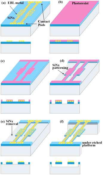
Figure 2. Schematic of the fabrication process with angled and cross-sectional views for the most important process steps described in the text.
Download figure:
Standard image High-resolution imageAnother optical lithography step with AZ6612 resist was carried out to selectively remove SiN using reactive ion etching (figures 2(c)–(e)). The SiN was under-etched using wet or dry etching (figure 2(f)). For wet etching, we used tetramethylammonium hydroxide (25% concentration for 30 min at 80 C) and subsequent replacement of solvent using isopropanol, which is then removed in a critical point dryer. Similar results were achieved using dry etching (deep reactive ion etching in
  plasma in an Alcatel AMS200 tool). An example of a fabricated heater/sensor device is shown in figures 1(a), (b).
2.2. NW growth
InAs NWs were grown using selective area epitaxy in a metal-organic chemical-vapor-deposition tool (Veeco). Si wafers with (111) orientation were pretreated by first dipping them into buffered hydrofluoric acid, followed by oxidation in air at 100  C for 20 min to form an oxide mask with pinholes. NW growth was carried out at 520
  C for 90 min using a tertiary-butyl-arsine flow of 20 μmol
  and a trimethyl-indium flow of 1.15 μmol
  . Under these conditions, InAs NWs grow perpendicular to the Si substrate along the
  direction with predominant zincblende crystal structure [36]. The resulting InAs NWs had a diameter
  nm and a total length of 4–5 μm. A transmission electron micrograph of one of these NWs is shown in figure 1(a). The NWs have a hexagonal cross-section with very low surface roughness. However, the crystal structure is affected by a multitude of stacking faults of the crystal planes perpendicular to the growth direction.
2.3. Positioning and contacting of NW samples
Figure 3 also shows images taken between different steps of the preparation procedure. The NW samples were positioned and contacted to the heater/sensor devices using a 3D-micro manipulator and a tungsten needle tip inside a combined electron microscope/focused ion beam (FIB) tool (FEI). Starting point was an under-etched MEMS heater/sensor structure as shown in figure 1(b). NWs were transferred onto a silicon oxide or SiN surface by tissue sweeping or stamping with polydimethylsiloxane (PDMS). Immediately after this transfer step the manipulation was started, because otherwise chemical binding forces or oxidation may lead to an increased adhesion of NWs to substrate which makes manipulation difficult. Individual NWs were picked up through adhesive forces using a tungsten needle, which was controlled using micromanipulators (Omniprobe). Typically the adhesion forces through van-der-Waals or electrostatic attraction is sufficient to adhere the NW to the tungsten needle. To influence the strength of adhesion between the needle and the NW, we used an electrically floating needle (negatively charged through the electron beam) during NW pick-up, and an uncharged needle (electrically grounded) while releasing the NW. During release of the NW onto the under-etched membranes the wire ends were touching the predefined leads near each heater/sensor, as shown in figure 3(b). At this stage, the two MEMS heaters/sensors were still connected through two bridges in the SiN membrane to provide additional stability during the NW placement (figure 3(b)).
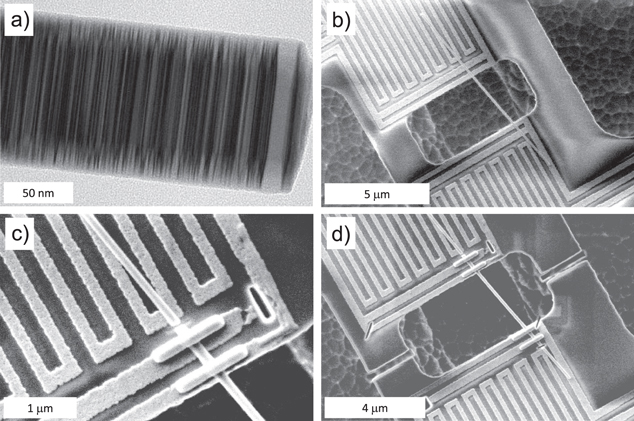
Figure 3. Images of a nanowire and of the key process steps of the nanowire placement and contacting as outlined in the text, and example of final measurement device with contacted sample. (a) Transmission electron micrograph of a similar nanowire; (b) scanning electron micrograph of the nanowire after placement; (c) detail of the contact region of the NW including two metal contacts and a cut separating the piece of NW extending into the heater region and (d) final device, after cutting of the nitride bridges between the heater/sensor platforms.
Download figure:
Standard image High-resolution imageThen, an electrically conductive contact was formed between the NW and the predifined leads (figures 3(c) and (d)). For this, the contact regions of the NW were first exposed to a well-controlled gallium-ion beam, such that only the native oxide layer of the NW was locally removed. Otherwise, care was taken to avoid ion-beam exposure of any other areas of the NW. To this end, all imaging steps were performed only with the electron beam of the dual-beam FIB tool. The contact regions were then metalized using ion-beam-induced deposition of platinum from an organo-platinum precursor (methylcyclopentadienyl (trimethyl) platinum). NW segments that extended too far into the heater region, were cut off using the focused gallium-ion beam (also shown in figure 3(c)). Finally, the SiN membrane bridges were cut using gallium-ion beam milling such that the MEMS heaters/sensors were connected to each other only via the NW. An example of a final device ready to be measured is shown in figure 3(d).
3. Experimental procedure
3.1. Principle of the thermal conductivity measurements
The thermal transport measurements using MEMS heaters/sensors rely on Joule heating and the temperature coefficient of resistance (TCR) to provide and measure a temperature gradient across the NW. The electrical four-probe resistance of the heaters was determined from current-voltage characteristics. For temperature calibration, the resistance in the limit of zero current was used. In this limit, it is safe to assume that the heaters/sensors have the temperature of the chip, which was measured independently. The TCR was determined for each heater separately by varying the chip temperature with the cryostat. It is assumed that Joule heating provides uniform temperature distribution on the heater platform.
In a typical measurement, the temperature of one heater/sensor ( ) is raised by applying a heating current (
 ) while its electrical resistances (
 ) is measured. Simultaneously, the temperature of the second heater/sensor (
 ) is determined by measuring its electrical resistance (
 ) using a small probing current (
 ). To determine the thermal conductance of the NW sample,
  , from the measurement, both the heater temperatures,
  and
and  , and the heat flux through the NW sample,
  , have to be determined (see figure 1 (d)). The heat dissipated in the heaters,
  and
and  , can be calculated from the respective heater currents and the electrical four-probe resistances. The two-probe resistance measured simultaneously allows us to determine the Joule dissipation in the electrical leads connecting to the heaters,
  and
and  . These electrical measurements of Joule dissipation and heater temperatures are related to the heat flux through the NW sample and thereby to the thermal conductance using the analytical treatment as described below.
The aspect ratio of the SiN platforms connecting the heaters to the carrier chip are so large that the application of the one-dimensional heat-diffusion equation is justified. In steady state, the heat-diffusion equation along the legs leading to heater 1 becomes,
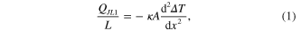
expressing the temperature distribution along the legs as the temperature rise  above ambient (or chip) temperature as a function of position x along the beam of length L. Here,
  is the Joule dissipation along the legs. The cross-sectional area A and the thermal conductivity κ comprise both SiN and metal leads and are therefore only effective numbers in this calculation that defines the thermal conductance of the legs,
  .
.
With the boundary conditions

(1) can be solved using

From this, we determine the total heat flow from the legs to the ambient for heater 1

and for the second heater accordingly. Next, we invoke energy conservation:


where we introduced the Joule heat dissipated in the heaters,  and
and  , and along the NW sample,
  .
.
The system of equations (4), (5) and (6) can be solved to obtain expressions for the conductance of the legs,  (assumed identical for both heaters) and of the NW sample,
  :
:


The difference to the previously reported [11] equations for  and
and  is that here the heating through the probing current
  is not neglected, giving rise to the second terms in (7) and (8). The better the devices are thermally decoupled, the more relevant the dissipation in the sensing heater becomes.
The Joule heat dissipated into the heaters is taken from the two-probe ( ) and four-probe (
 ) resistance measurements, and we define an effective heater power (omitting the index for heater 1 and 2) as

3.2. Measurement setup
The heat conductance measurements were performed with a dc technique. The heater (H1) was driven with constant heating current  (swept typically between 0.1 μA and 10 μA) using the outer electrodes of the four-probe temperature sensor. The voltage drops across the inner (four-probe) and outer electrodes (two-probe) were measured simultaneously using two voltage meters (Keithley DMM 196). Two measurements with reversed polarity of
  were performed to eliminate thermoelectric offsets. In addition,
  was measured with a high-resolution electrometer (Keithley 6517) to improve accuracy. While applying a constant heating current to H1, the resistance of the four-probe temperature sensor (H2) was measured using a Keithley Delta Mode system consisting of a 6221 dc and ac current source and a 2182A nanovoltmeter. A constant sensing current
  of typically 100 nA was applied to the heater with a resistance in the 1–
 range, low enough to avoid self-heating of the sensor. The polarity of the current was reversed after a period of 200 to 500 ms to cancel out thermo-electric offsets. Afterwards, the Seebeck voltage across the NW was measured at each heater power using the nanovoltmeter connected to the inner NW contacts. Thermoelectric offsets of the circuitry were determined and subtracted as well. Subsequently, the roles of H1 and H2 were swapped and the measurement was repeated.
All measurements were performed in a cryo-probestation at a vacuum of  (
( ). The temperature of the sample was measured with a calibrated Si-diode mounted on the surface of the test chip. Temperature stability of the sample was typically better than 0.1 K at any set temperature between 150 K and 350 K. Shielded electrical contacts to the test chip were provided by a 16-pin probecard connected to a 8 × 24 switching matrix (Keithley 7172).
3.3. Temperature calibration
The measurements of the thermal conductivity and the Seebeck coefficient require the precise determination of the temperature of the two heater platforms. Heater/sensor temperatures were determined from the TCR of the resistive coils measured by four-probe technique at a series of substrate temperatures. The current applied to read out the temperature, however, leads to an increase of temperature because of the high thermal resistance of the heater structures. On the other hand, the use of extremely small sensing currents induces only a marginal voltage drop across the heater and, hence, results in an inferior signal-to-noise ratio. Therefore, for calibration, the electrical resistances were determined in the limit of zero dissipated electrical power for each substrate temperature. It turned out, to a good approximation, that the electrical resistance increases linearly with the effective heater power. Therefore, the electrical resistance measured by extrapolating the linear resistance-power plot to zero corresponds to the temperature of the substrate. The standard deviation of typical measurement series was usually below 0.05 K.
Figure 4(a) shows the temperature increase in the heater and the sensor as a function of the effective heater power given in (9) at a substrate temperature of 300 K. Both directions (H1 as a heater, H2 as a sensor, and vice versa) are equivalent within an uncertainty of 0.1 K in the measured temperature difference.

Figure 4. Example of thermoelectric measurement extracted from a single current sweep. (a) The temperature increase induced in the heater (triangles) is a accompanied by a temperature increase in the sensor (squares). Swapping the roles of heater and sensor (colors) produces the same trend. From these measured temperatures and the Joule dissipation during the measurement, the thermal conductance of the sample can be extracted using (8) (see text). (b) Seebeck voltage probed at the ends of the NW as a function of the temperature difference between heater and sensor, measured simultaneously with (a). The Seebeck coefficient is then extracted from the slope of the linear fit, which is independent of the heating direction. The contribution of the Au leads (approximately +2 μW  ) was neglected.
Download figure:
Standard image High-resolution image4. Experimental results
A series of InAs NWs with diameters between 100 nm and 150 nm was investigated. After mounting a sample into the cryo-probestation, the temporal stability of the resistance of the heater/sensor was monitored and enhanced by application of an electrical current, leading to a burn-in of the resistor. This step was performed for typically 1 h at 350 K using a current of the order of 1 μA. At various substrate temperatures, the heater current  was ramped from 0.1 μA to 10 μA and back. Both the two-probe (
 ) and the four-probe (
 ) resistance of the heater as well as the four-probe resistance of the sensor (
 ) were measured as a function of the heater power
  for each substrate temperature. The Seebeck voltage across the NW was measured simultaneously. Each measurement was repeated, swapping the roles of sensor and heater between heater/sensor H1 and H2.
4.1. Thermal conductance measurements
Having determined the temperature rise of heaters according to the calibration routine, the thermal conductances of the heater/sensor leads,  , and the NW sample,
  , can be calculated using (7), (8) and (9). The data for each substrate temperature were averaged and are reported in figure 5. The thermal conductance of the measurement device (
 ) is significantly lower than the resulting values for previously measured NWs [16]. Such devices are therefore promising for ultra-low thermal conductance measurements. The noise limit of the device and the measurement apparatus was estimated using the scatter of conductance data of the NW for a given substrate temperature because all measurement errors enter these data and are expected to induce scatter of the data. The one-sigma scatter of the data was below 0.2 nW
  .
.

Figure 5. Thermal conductances of the measurement MEMS device ( ) and the InAs NW sample (
 ). Each data point uses an average over different data points of curves such as those in figure 4(a). The scatter bars show the standard deviation of the average. Both directions of heat flow are averaged.
Download figure:
Standard image High-resolution imageThe thermal conductance of the heater/sensor legs,  , compares well with the expectations. For the particular design we used, the thermal resistance can be estimated from the dimensions. Two 300 μm long, 3 μm wide and 150 nm thick SiN membranes carry three metal lines with a width of 250 nm and a thickness of 50 nm. With typical values of thermal conductances of SiN (4 W
  ) and Au (100 W
  ) for thin films at room temperature [37, 38], we obtain 35 nW
  , in agreement with our experimental data. Other devices with leg lengths of up to 0.75 mm allowed the value of
  to be reduced down to 20 nW
  at room temperature. The slight increase of the thermal conductance
  with temperature is expected for thin metal films. The NW used in this experiment had a length of 2.75 μm and a diameter of 125 nm. Its thermal conductance
  exhibited a weak temperature dependence with a magnitude of about 12 nW
  averaged over both signs of the temperature gradient.
4.2. NW Seebeck voltage and electrical conductance measurements
The Seebeck coefficient (thermopower) was determined from the slope of the Seebeck voltage plotted against the temperature difference between the heater/sensor platforms as shown in figure 4(b). Here, both signs of the temperature gradient are plotted. The four-probe electrical resistance of the NWs was determined from measured current–voltage diagrams, taking the resistance value extrapolated to zero current. The extrapolation was done to ensure that the temperature of the wire is the temperature of the chip.
5. Discussion
Figure 6 shows the complete thermoelectric data of a single InAs NW as a function of the substrate temperature. The NW in this example had a length of  , and diameter of 125 nm. Thermal conductivity and electrical conductivity were calculated from the measured conductances and the dimension of the NW as inferred from electron microscopy. However, it is very likely that the carrier concentration is not uniform along the radius of the NW. Typically, the region close to the surface of nominally undoped InAs NWs has a higher conductivity due to Fermi level pinning [34]. As both Seebeck coefficient and conductivity strongly depend on the carrier concentration, comparison with values from other experiments is difficult. For this particular NW, we can extract a power factor of
  = 4.6 μW (
 m)−1 and a figure of merit ZT =
  = 5.4
= 5.4  at 300 K. The power factor of this InAs NW is considerably lower than typical values of similar NWs [26]. While the magnitude and the temperature dependence of the Seebeck coefficient follow the expected trend for degenerate InAs [7], the electrical conductivity is relatively low and exhibits the thermally activated behavior of a lowly-doped semiconductor. We attribute this to a reduced mobility due to surface charges and defects of the unprotected NW, which were probably induced by the electron beam during the imaging when placing the NW on the heater platform.

Figure 6. Full thermoelectric characterization of single InAs NW sample. (a) The Seebeck coefficient is taken as the slope of curves such as those shown in figure 4(b). (b) Electrical resistivity calculated from the measured four-probe resistance and the dimensions of the NW. (c) Thermal conductivity calculated from the measured thermal conductance in figure 5 and the NW dimensions. The error bars show the standard deviation of the averaged ensemble of data points measured at various points of the curves in figure 4(a) and for both heating directions.
Download figure:
Standard image High-resolution image
The thermal conductivity, however, deviates significantly from the bulk value. With a variation of ≈10%, it is almost independent of the temperature in the measured range. This is typical for nanostructures in the regime of boundary scattering as predominant phonon-scattering mechanism. We investigated about 10 NWs with diameters between 100 nm and 150 nm, yielding thermal conductivities in the range 2.5±1 W  . The magnitude is significantly lower than the bulk value as expected for nanostructures in which phonon boundary scattering is significant (for example, measurements of thermal conductance in InAs nanoribbons [35]). However, the conductivity extracted is significantly lower than the value obtained for single-crystalline InAs NWs of both wurtzite and zincblende structures [16], or calculations of phonon conductance in InAs NWs [22]. Due to the different growth mode, our wires are neither purely wurtzite or zincblende. Instead, a multitude of stacking faults lead to a polycrystal of wurtzite and zincblende segments with a broad length distribution (see figure 1(a)). The segment length range from tens of nanometers down to almost a single nanometer. We attribute the lower thermal conductivity in our wires (reduced by a factor of about 3) to these stacking faults. We exclude that the discrepancy is caused by an additional thermal resistance at the contacts to the NW for three reasons: first, we consistently measure a lower value for all devices. Secondly, we varied the contact area without any significant change in the value extracted, as described above. Thirdly, we obtained very similar values using the self-heating method of the same wires. The self-heating method is less influenced by thermal boundaries [10]. Furthermore, as mentioned above, we can exclude amorphization of the InAs through interaction with the ion beam, because ion-beam exposure was limited to the contact regions to the metal electrodes. A small amount of carbon deposition during scanning electron microscopy cannot be excluded but is not expected to lead to a strong reduction of thermal conductance.
The conclusion that the stacking faults significantly reduce thermal conductivity is interesting, because stacking faults such as twin boundaries are interfaces with very similar materials on either side, namely the same constituents with just a different stacking order. This effect can therefore not be easily described using classical models of thermal interfaces. Although the thermal impedance mismatch between the two phases is minimal, there is yet some induced scattering at the interfaces expected [39]. Furthermore, periodicity is destroyed on a length scale larger than a few nanometers (the closest distance between twin boundaries) such that longer range phonon cannot propagate. The observation may be of technological relevance if through the randomly distributed twin boundaries the phonon transport is reduced by a different amount than the electron transport. The current samples, however, are unpassivated and therefore surface charge and surface defects limit the electron mobility. Future experiments on passivated devices will be of interest in view of thermoelectric energy conversion.
Acknowledgments
The research leading to these results has received funding from the European Union Seventh Framework Programs (FP7/2007-2013) NANOHEAT under grant agreement no. (318625), STEEPER no. (257267), the Marie Curie Actions-Intra-European Fellowship (IEF-PHY) WISE under grant agreement no. (276595), TETTRA and the IBM Research Far Reaching Research program. We acknowledge support and stimulating discussions from Kevin Lister, Emanuel Loertscher, Michel Despont, Walter Riess, Meinrad Tschudy, Andreas Bischoff, and Andreas Schade as well as Aghababaei Ramin and Guillaume Anciaux (phonon scattering calculations).