
Abstract
As metal nanorods show much higher metal enhanced fluorescence (MEF) than metal nanospheres, microfluidic-based MEF is first explored with Ag nanorod (ND) arrays made by oblique angle deposition. By measuring the fluorescein isothiocyanate (FITC) solution sandwiched between the Ag NDs and a piece of cover slip, the enhancement factors (EFs) are found as 3.7 ± 0.64 and 6.74 ± 2.04, for a solution thickness at 20.8 μm and 10 μm, respectively. Because of the strong plasmonic coupling between the adjacent Ag NDs, only the emission of the fluorophores present in the three-dimensional NDs array gets enhanced. Thus, the corresponding effective enhancement factors (EEFs) are revealed to be relatively close, 259 ± 92 and 340 ± 102, respectively. To demonstrate the application of MEF in microfluidic systems, a multilayer of SiO2 NDs/Ag NDs is integrated with a capillary electrophoresis device. At a microchannel depth of 10 μm, an enhancement of 6.5 fold is obtained for amino acids separation detection. These results are very encouraging and open the possibility of MEF applications for the Ag ND arrays decorated microchannels. With the miniaturization of microfluidic devices, microfluidic-based MEF by Ag ND arrays will likely find more applications with further enhancement.
Export citation and abstract BibTeX RIS
1. Introduction
Metal enhanced fluorescence (MEF) refers to the phenomenon in which when the fluorophores are in close proximity to metal nanostructures, the fluorescence emission is greatly enhanced. The enhancement is mainly due to the strongly intensified local electric field around the nanostructures by localized surface plasmon resonance (LSPR) [1–3]. The strength of the field exponentially decreases with the distance away from nanostructures. Thus the enhancement normally takes place within the distance of a few nanometers to hundreds of nanometers, depending on the morphology of the nanostructures [4–6]. MEF has been well applied for biosensors and bioimaging [7–10], but little attention has been given to microfluidic-based applications, which can provide a solution environment for biomolecules and compensate for the signal loss with the reduced number of analytes. The lack of research may be attributed to the fact that it is difficult to control the distance between the fluorophores and metal nanostructures in the microfluidic environment. A few attempts have been made through droplet control or analyte-nanoparticle conjugation. By confining Ag colloids and fluorescence dye–labeled proteins in a droplet micromixer, a maximum enhancement of 35 fold is found at a particle concentration as high as 1013 ml−1 and a proper salt concentration. Without salt, the enhancement is only two- or threefold [11]. By tailoring the inter-distance of the Au nanosphere and quantum dot conjugates in the capillary electrophoresis (CE) microchannel, a maximum enhancement of 2.3 fold is observed [12]. These works have shown integration between MEF and microfluidics but with non-uniformity and limited enhancement.
Recently, more and more studies reveal that the nanorods (NDs) or nanowires (NWs) have a much higher MEF enhancement than nanospheres. A few experimental works have reported the near-field enhancement from 33 to 100 fold [12–16]. Some works even show over a thousand-fold enhancement for single molecule fluorescence detection [17]. In addition, a theoretical study has concluded that the local electric field enhancement around NDs or NWs is at least one order of magnitude larger than that around nanospheres [18]. However, if use is made of ND or NW aggregates or conjugates directly in microchannels, they could easily clog the channels due to their large aspect ratio. An alternative way is to immobilize the NDs or NWs onto microchannel inner walls and have them extruded from the walls. Since the spacing between the adjacent NDs or NWs is within the MEF enhancing distance, the analytes freely flowing through the 'forest' of NDs or NWs will get their fluorescence intensity enhanced. Reasonably, uniform nanostructure arrays are desired to ensure a reproducible enhancement across the microchannel. The challenges lie not only in the MEF enhancing ability of the NDs or NWs, but also in their fabrication and integration methods. Solution-based chemical synthesis is the most mature technique for fabricating metal NDs and NWs. It possesses the merits of good control of size and shape, low cost, and easy fabrication. However, the metal NDs or NWs prepared by this technique present the difficulty of decorating the channel walls in such a way that they protrude and penetrate into the solution [12, 13]. Electron beam lithography can be used to fabricate regular nanostructure arrays, but it is still not practical to build up extruded metal nanostructures. Furthermore, it often involves very costly and difficult processing steps [14, 19].
In this study, we employ the oblique angle deposition (OAD) technique to fabricate Ag NDs. OAD is a physical vapor deposition method, where the regularly arranged three-dimensional NDs arrays are self-aligned on the substrate due to a shadowing effect and adatom diffusion [20, 21]. As shown in figure 1(a), in an electron beam evaporator the substrate holder is connected with a motor and tilted at a large deposition angle  , defined as the angle between the surface normal and the incoming vapor. At the beginning of the deposition, nuclei with different heights form on the surface. As the deposition proceeds, shorter nuclei are blocked by the taller ones and left as the voids between the nanorods grown. In addition to the convenient fabrication of three-dimensional metal ND arrays on the substrate, Ag NDs made by OAD have shown enormous sensitivity for surface-enhanced Raman spectroscopy, due to the strong LSPR coupling between adjacent NDs [22, 23]. Furthermore, the Abdulhalim research group has applied OAD for MEF-improved bio-imaging. They coat 50 nm–thick fluorescent dye Rhodamine 123 onto Ag NDs and find the highest enhancement of 15 with respect to Ag film, while the enhancement in other MEF literature only refers to the bare Si or glass substrates [10]. Therefore, Ag NDs made by OAD have great potential in developing MEF-enhanced microfluidic applications.

Figure 1. Schematics descriptions: (a) Oblique angle deposition of Ag NDs. (b) MEF measurement set-up (top view). (c) Integration of Ag NDs into capillary electrophoresis (CE) microdevice.
Download figure:
Standard image High-resolution imageHere, we first studied solution-based MEF measurements from Ag NDs made by OAD in terms of their morphology, orientation, and optical properties. Then, we investigated the effective enhancement only from the fluorophores interacting with Ag NDs. Finally, we integrated the Ag NDs with a CE device and explored the MEF-improved amino acids separation detection.
2. Methods and materials
2.1. Ag ND depositions by OAD
Prior to the depositions, Si substrates 1.5 cm by 1.5 cm were sonicated in acetone, ethanol, and deionized (DI) water and then dried by nitrogen. To enhance the adhesion between the Ag NDs and Si substrates, a thin layer of Ti film with a thickness of 10 nm was evaporated onto the Si surface at the deposition angle  . After that, Ag NDs with five nominal thicknesses
  nm, 500 nm, 1000 nm, 2000 nm, and 3000 nm were deposited at the deposition angle
  . For comparison, Ag film with a thickness of 500 nm was deposited on the Si substrate at the deposition angle
  . A quartz crystal sensor was used to monitor the thickness. The background pressure was about 8 × 10⁻⁷ Torr. Ag and Ti were both at 99.99% and were purchased from Kurt J Lesker.
2.2. MEF and optical measurements
The MEF of fluorescein isothiocyanate (FITC, Invitrogen) was studied using sandwich geometry. A droplet of 3 μl FITC dissolved in phosphate buffered saline (PBS, PH 7.4, Gibco) solution at a concentration of 10−4 M was applied onto the Ag ND sample surface. Immediately, a cover slip with an area of 12 mm by either 12 mm or 25 mm was placed on the droplet, and the sample was sealed with grease before an optical measurement was performed right away. This led to an FITC solution thickness on the Ag NDs that was calculated to be either  μm or
μm or  μm, depending on the cover slip size employed (figure S1, supporting information, available at stacks.iop.org/NANO/25/225502/mmedia). As will be seen later, these calculations using simple geometry turned out to be reliable estimates of the solution thickness, as the registered enhancement values, in particular with
  μm, agreed reasonably well with the values from CE devices fabricated with a well-defined thickness. For reference, Ag film deposited on a Si wafer and a bare Si wafer were used and subjected to the same test samples and measurement steps as with the Ag NDs. These measurements were then used to normalize those from the Ag NDs. The chips were examined by Luminescence Spectrometer LS 50 B (Perkin Elmer) using the fluorescence measurement set-up shown in figure 1(b). As can be seen, the excitation wavelength was selected by a built-in select filter, and the stray light was filtered out by a 488 nm narrow band pass filter. The light source and the signal collection were arranged in a right-angle configuration. A homemade sample holder was utilized to make the incident angle on the sample chip equal to 60° to deviate the specular reflection from the collection path. Further adjustment of slit 1 and slit 2 ensured that no reflection from the sample chip entered the collection. Reflection and scattering spectra were measured by a reflection stage (STAGE-RTL-T, Ocean Optics). Reflection spectra were taken by a 45° incidence and collection configuration. Scattering spectra were measured by a 60° incident angle. The light source was a Xenon lamp, and the spectra were collected by Ocean Optics USB 4000.
2.3. CE Device fabrication and integration with NDs
Through a deposition mask, a strip of SiO2 NDs/Ag NDs with 2 mm width was selectively deposited on the glass substrate. Then, to avoid the adsorption of biomolecules to the Ag surface, a very thin layer of SiO2 shell was conformally coated onto the Ag NDs by following Song's work [24, 25]. In brief, the Ag NDs were first immersed in citric acid for half an hour to obtain citric groups on the surface. Then the chips were immersed in a mixture of tetraethyl orthosilicate (TEOS), EtOH, and H2O for 20 min. As a catalyst, ammonium hydroxide was added to the mixture to initiate the reaction, and the coating thickness was controlled by the reaction time. Citric acid, TEOS, and EtOH were purchased from Sigma-Aldrich, while SiO2 (99.99%) was from Kurt J Lesker.
The sample injection and separation channels were molded in Poly(dimethylsiloxane) (PDMS, Sylgard 184, Dow Corning) following the standard soft lithography procedure. Both were 20 μm wide and either 10 μm or 40 μm deep depending on the corresponding SU8 master. Four reservoirs to access the channels, each with a diameter of 2 mm, were punched through the PDMS slab (Harris Uni-Core, TED Pella, Inc.). The channels were enclosed through bonding over the glass substrate with the Ag ND strip perpendicular to the end of the separation channel, as shown in figure 1(c). All the bonding procedures were accomplished through activating the respective surfaces in oxygen plasma (29.6 W Harrick Plasma) for 45 s.
2.4. CE preparation
The buffer solution, sodium tetraborate decahydrate (borate, Sigma-Aldrich), was prepared to the concentration of 10 mM in deionized (DI) water and passed through a membrane filter (0.22 μm pore size, Millipore). Two amino acids, Arginine (Arg) and Glycine (Gly), were individually dissolved in the buffer to the concentration of 1 mM and fluorescently labeled by combining with 1 mM fluorescein-5-isothiocyanate (FITC) in acetone at 100:1 (v v−1) overnight in the dark. Before analysis, the amino acids were mixed at 1:1 (v v−1) and diluted to 10 μM in the buffer (pH 10.2).
2.5. CE experiments
The experiments were conducted under an epi-fluorescence microscope (FN1, Nikon) equipped with a mercury lamp (100 W) as well as the filter cube for FITC (Ex/Em 492/520 nm) detection. The platinum electrodes connected to a high-voltage power supply (Tianjin Dongwen Co., Ltd., China) were immersed into the reservoirs and individually controlled by the Labview. Prior to the experiment, the device was rinsed with DI water and filled with buffer solution. The gated sample injection and electrophoretic separation were realized by the voltage protocol described previously [26]. Time-resolved video frames were captured through a 10 × objective and stored in a computer through a CCD camera (RT3 Mono, SPOT). Electropherograms were generated and analyzed with image processing software (ImageJ; NIH, Bethesda).
3. Results and discussion
3.1. Morphology
Scanning electron microscopy (SEM) images of Ag NDs with distinct nominal thicknesses are shown in figure 2. As can be seen, when the nominal thickness  is only 300 nm, random Ag nano-islands appear on the substrates. At
  nm, these nano-islands become elongated. At
  nm, elongated Ag NDs start to stretch out of the surface. At
  nm and 3000 nm, tilted Ag NDs with a large aspect ratio form on the surface. The features of the Ag NDs measured directly on the SEM images are listed in table 1, where
  and
and  are the diameter and length of the individual Ag NDs, respectively, the aspect ratio is the ratio between the length and diameter,
  is the tilt angle between the substrate surface normal and the Ag NDs' growth direction, and
  is the Ag NDs' surface density. As the nominal thickness increases, the aspect ratio increases until
  nm. The slight decrease of the aspect ratio at
  nm is due to a large increase in the diameter. This is because the lateral diffusibility of Ag adatoms becomes high, as the chamber temperature increases with the deposition time.

Figure 2. SEM images of Ag NDs (top and cross-sectional views) with a nominal thickness at (a) 300 nm, (b) 500 nm, (c) 1000 nm, (d) 2000 nm, and (e) 3000 nm. The scale bar is 200 nm.
Download figure:
Standard image High-resolution imageTable 1. Features of Ag NDs with a varying nominal thickness (further defined in figure 4(b)).
Nominal thickness  (nm) (nm) |
Diameter  (nm) (nm) |
Length  (nm) (nm) |
Aspect ratio | Tilt angle 
|
Density  (count
μm−2) (count
μm−2) |
|---|---|---|---|---|---|
| 300 | 70 ± 12 | 146 ± 48 | 2.1 | N.A. | 30 ± 0.3 |
| 500 | 58 ± 8 | 249 ± 30 | 4.3 | N.A. | 35 ± 0.6 |
| 1000 | 78 ± 8 | 595 ± 98 | 7.6 | 74° ± 4° | 23 ± 1.0 |
| 2000 | 89 ± 33 | 1125 ± 186 | 12.6 | 72° ± 3° | 18 ± 1.2 |
| 3000 | 148 ± 23 | 1749 ± 180 | 11.8 | 70° ± 3° | 17 ± 0.6 |
3.2. MEF and optical measurements
Considering that Ag NDs are anisotropic, fluorescence spectra are taken from four distinct orientations ( ,
,  ,
,  , and
, and  ) as schematically described in figure 3(a). In each orientation, since enhancement shows the same trend over the range of nominal thickness values
  , figure 3(b) plots enhancement factors (EFs) measured only in orientation
  for the solution thickness
  μm on nine distinct Ag ND substrates involved for each thickness value. The
  are simply defined as the ratio of the fluorescence peak intensity of the sample obtained on the Ag NDs to that on a reference substrate (bare Si or Ag film on Si). The
  referenced to Si substrate are typically higher in mean values and variations since the obtained reference intensity is weaker. Meanwhile, the reference intensity from Ag film is larger due to a constructive interference of the incident and reflected emissions of the fluorophores near the film surface [27]. This makes the
  referenced to Ag film lower in comparison. As shown, the Ag NDs at
  nm give the highest
  , 3.7 ± 0.64 and 1.3 ± 0.23, as referenced to Si and Ag-film substrates, respectively. The lowest
  belongs to the Ag NDs at
  nm. Figure 3(c) further reveals the
  measured in four distinct orientations for those at
  nm. Among those with the solution thickness
  , standard deviation of the
  , considering only those referenced to Si substrate and averaged over each orientation, is merely 0.74, indicating that the orientations of the Ag NDs do not greatly alter the enhancement. As discussed in the Introduction, MEF is a short-range effect and mainly takes place in the region very close to nanostructures. To further investigate the short-range effect, figure 3(c) also presents
  measured in each orientation for the solution thickness
  μm on six distinct Ag ND substrates at
  nm. Apparently, with a reduced solution thickness, the
  referenced to Si substrate noticeably increases, signifying that only the fluorophores close to the Ag NDs get an enhanced emission. In contrast, such a short-range effect is not immediately evident in those referenced to Ag-film substrate, mostly because of the constructive interference that leads to a larger-intensity contribution regardless of the reduced solution thickness.
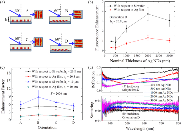
Figure 3. (a) Four distinct orientations of Ag NDs for the solution-based MEF measurements. (b)  of the Ag NDs at T = 300 nm, 500 nm, 1000 nm, 2000 nm, and 3000 nm with reference to Si and Ag film substrates. The measurements were performed with orientation
  and the solution thickness at
  μm. (c)
  of the Ag NDs at
  nm and with different orientations and solution thicknesses. (d) Reflection and scattering spectra of the Ag NDs at T = 300 nm, 500 nm, 1000 nm, 2000 nm, and 3000 nm, measured with 45° and 60° incidence (orientation
  ), respectively.
Download figure:
Standard image High-resolution imageTo understand the relationship between the  and the optical properties of Ag NDs, reflection and scattering spectra are obtained by dividing the specular data by an incident spectrum taken from the reflection of Ag film. Thus, the reflection or scattering spectra are only presenting the characteristic peak positions as well as the relative intensities from Ag NDs with different morphology or nominal thickness. There is no quantitative connection between the reflection spectrum and the scattering spectrum. As shown in figure 3(d), at
  nm, Ag nano-islands have an absorption peak around 428 nm. When the thickness increases to 500 nm, the absorption peak becomes broader and red shifts to 510 nm, which is well overlapped with the emission maximum wavelength of FITC. Therefore, it may account for the lowest MEF enhancement. Ag NDs at
  nm have no significant absorption peak, while those at
  nm and 3000 nm all show an absorption peak at 378 nm, consistent with the literature [28]. As known, the fluorescence intensity will be enhanced if the emission wavelength of fluorophores matches the scattering wavelength of nanostructures [1]. To make the analysis consistent with the results shown in figure 3(b), the scattering spectra were taken with orientation
  . According to the spectra, the Ag NDs, except those at T = 300 nm, show a broad scattering peak with the peak position around 470 nm, and the intensity increases with the nominal thickness. The peak is so broad that the scattering intensity at 510 nm is similar to that at 470 nm. Therefore, the
  generally increase as the nominal thickness of the Ag NDs increases. The discrepancy between Ag NDs at
  nm and
  nm will be discussed in the next section. The reflection and scattering spectra for the other measurement orientations exhibit similar trends (figure S2, supporting information).
3.3. Effective enhancement factors
In the solution-based MEF measurements, the enhancement comes only from the region where the electric field is intensified around Ag NDs, while the fluorophores outside this region will not be affected. Figure 4(a) shows the electric field distribution around 12 isolated Ag NDs simulated in Comsol 4.3b with the dimensional conditions at  nm. The p-polarized beam incidents at an angle of 60° onto the Ag NDs with orientation
  . The plot shows the corresponding electric field enhancement, defined as the ratio between the enhanced field
  and the incident field
  , for the cross-sectional profile along the line from A to B. As can be seen, the field enhancement exponentially drops to 1 when the distance away from the outer Ag NDs is 135 nm or 96 nm, while the enhancement between the adjacent Ag NDs is always high due to the strong LSPR coupling. Considering that there is a continuous layer of Ag NDs instead of isolated ones, the enhancement mainly takes place in the voids of the Ag ND layer. As schematically shown in figure 4(b), we denote the Ag ND layer as the effective region and the volume of the FITC solution filling the layer as the effective volume (VEff
). The effective enhancement factor (EEF) is then defined as the ratio between
, for the cross-sectional profile along the line from A to B. As can be seen, the field enhancement exponentially drops to 1 when the distance away from the outer Ag NDs is 135 nm or 96 nm, while the enhancement between the adjacent Ag NDs is always high due to the strong LSPR coupling. Considering that there is a continuous layer of Ag NDs instead of isolated ones, the enhancement mainly takes place in the voids of the Ag ND layer. As schematically shown in figure 4(b), we denote the Ag ND layer as the effective region and the volume of the FITC solution filling the layer as the effective volume (VEff
). The effective enhancement factor (EEF) is then defined as the ratio between  and
and  , where
  and
and  are the fluorescence intensity values attributed to the molecules in the effective volume
  with and without the Ag NDs, respectively. We assume that FITC molecules are uniformly distributed in the solution, thus
  can be taken as the measured reference fluorescence intensity,
  , multiplied by a fraction of the total volume
  enclosed in
  . Accordingly, IAg − Eff
can be calculated by deducting from the measured intensity of Ag NDs, IAg, the fluorescence intensity of the non-effective volume. Since the fluorescence intensity distribution for Ag film is not uniform, as stated previously, here we only calculate the
. Accordingly, IAg − Eff
can be calculated by deducting from the measured intensity of Ag NDs, IAg, the fluorescence intensity of the non-effective volume. Since the fluorescence intensity distribution for Ag film is not uniform, as stated previously, here we only calculate the  referenced to Si substrate using the following formula [29]:
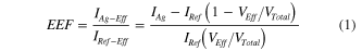
Figure 4. (a) Simulated electric field enhancement around Ag NDs at T = 2000 nm. (b) Illustrations: the MEF effective region and intensity relationship for Ag NDs and Si reference (left panel), as well as the structural features of the Ag NDs (right panel).
Download figure:
Standard image High-resolution imageSubstituting  ,
,  can be rearranged as,

Both the effective volume  and the total volume
  can be calculated as:


where  and
and  refer to the height and the surface area covered by the Ag ND layer, respectively. Table 1 lists the values of
  ,
,  ,
,  , and
, and  as measured on the SEM images. A schematic description of these features is also given in figure 4(b).
Table 2 summarizes the  and
and  of the Ag NDs at the nominal thickness
  nm and
  nm and with the solution thickness
  μm and
  μm. Mean and standard deviation values are taken over four different measurement orientations. For the Ag NDs at
  nm and with
  μm and
  μm,
μm,  are found to be relatively close, 259 ± 92 and 340 ± 102, respectively. For the Ag NDs at
  nm, however, a larger value of
  , 494 ± 157, is noticeable possibly due to their higher scattering intensity. Although the Ag NDs at
  nm present a larger
  than those at
  nm, they have a smaller
  (
( nm) because of their reduced effective volume fraction
  . This can clearly be seen from equation (2), in simplified form
  or
or  as the volume fraction
  is extremely small.
Table 2.
Mean and standard deviation (SD) values of  and
and  of Ag NDs.
 (nm) (nm) |
 (μm) (μm) |

|
Mean 
|
SD | Mean 
|
SD |
|---|---|---|---|---|---|---|
| 2000 | 20.8 | 1.07% | 4.63 | 1.09 | 259 | 92 |
| 2000 | 10 | 2.22% | 6.74 | 2.04 | 340 | 102 |
| 3000 | 20.8 | 0.42% | 3.06 | 0.66 | 494 | 157 |
3.4. Fluorescence enhanced amino acids capillary electrophoresis
The Ag NDs integrated in microfluidics have been characterized by their fluorescence enhancement performance in electrophoretic separation of amino acids. To avoid the physical adsorption of amino acids onto the Ag surface, a layer of 4 nm SiO2 shell is conformally coated onto Ag NDs. Figure 5(a) shows the transmission electron microscopy (TEM) images of Ag NDs with different SiO2 shell thicknesses. In the preliminary experiments, an encountered problem is that the Ag ND layer is easily oxidized, generating bubbles in response to the applied high-separation voltage. This suggests that the Ag ND layer sustains an induced electrical current possibly due to shorting of the Ag nano-islands that led to the individual Ag NDs. To overcome this problem, the Ag NDs (2000 nm) were deposited on a layer of 200 nm SiO2 NDs as shown in figure 5(b). In return, the individual Ag NDs are well isolated and manage to resist oxidation.
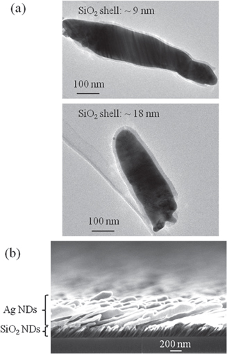
Figure 5. (a) TEM images of SiO2-coated Ag NDs with shell thicknesses at 9 and 18 nm. (b) SEM cross-sectional image of the multilayer SiO2/Ag NDs.
Download figure:
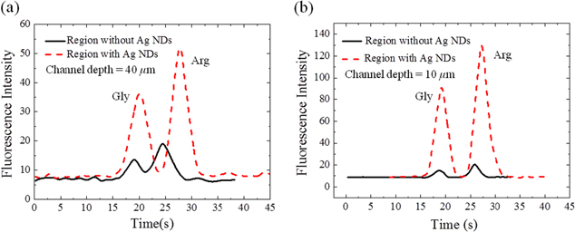
Standard image High-resolution imageFigure 6(a) shows the representative electropherograms for the electrophoretic separation of the two amino acids through a CE separation channel with a depth of 40 μm. The peaks are resolved with ease within 40 s at a migration time of 18.7 s and 25.9 s for Arg and Gly, respectively. As can be seen, the amino acids detected at the site of the Ag ND layer show a significant fluorescent enhancement by about 2.5 fold as compared to their peaks detected at a nearby upstream site where there is no Ag ND layer. As a result of a short distance between the two detection sites (∼500 μm), the migration time of the corresponding peaks is slightly shifted. The separation efficiency can be evaluated based on the resolution  and the number of theoretical plates
  according to the following definitions [30]:


where  refers to the time interval between the two separated peaks, each with a width of
  and
and  , whereas
  and
and  refer to the migration time and baseline width of a specific peak of interest.
Figure 6. Electropherograms for the analysis of a mixture of two FITC-labeled amino acids through the separation channels of a height (a) 40 μm and (b) 10 μm, both under 300 V cm−1. The regions with and without Ag NDs refer to distinct detection points apart by ∼500 μm along the separation channels.
Download figure:
Standard image High-resolution image
It is found that the resolution slightly increases from 1.01 ± 0.10 to 1.24 ± 0.04 with Ag ND. The theoretical plate numbers show only a slight variation from 1800 ± 74.88 to 1600 ± 60.26 for Arg and from 2300 ± 206.37 to 2400 ± 94.70 for Gly. In other words, with the integration of the Ag NDs, the separation efficiency is maintained. A similar trend is also observed in the separation channel 10 μm deep and yet with a higher fluorescent enhancement of 6.5 fold as shown in figure 6(b). This level of enhancement is comparable to that encountered in the Ag ND chips with 10 μm solution thickness. Further analysis shows that the reduced channel depth notably improves the separation resolution to 3.68 ± 0.18 and 3.11 ± 0.12 as detected on the sites with and without the Ag NDs, respectively. On the same sites, the plate numbers vary slightly, 1100 ± 72.84 and 1200 ± 80.74 for Arg while 2300 ± 140.55 and 1800 ± 146.06 for Gly, respectively. All the standard deviations reported are based on five repeat runs.
The above results show that the separation detection in microfluidic CE can be improved owing to the strong MEF coupling of Ag NDs. As expected, the enhancement is inversely proportional to the depth of the microchannel as a result of the short-range MEF effect. In fact, further miniaturization of the separation channel will improve the separation efficiency by reducing Joule heating [26]. In such a case, the MEF of Ag NDs could facilitate the separation detection further. In our research, the integration of Ag NDs with CE devices having further reduced separation channels is under investigation.
4. Conclusion
We have studied the solution-based MEF property of the Ag ND arrays made through OAD in terms of their morphology, orientation, absorption, and scattering. When the thickness of the sandwiched solution is 20.8
μm, the Ag nano-islands at the nominal thickness  nm and 500 nm offer small
  as a result of weak scattering or wavelength overlapping between the LSPR absorption and FITC emission. As the nominal thickness increases to 2000 nm, Ag NDs exhibit the largest
  , and their varying orientations do not greatly influence the
  values. Since MEF is a short-range effect and only occurs within interstitial spaces in the Ag ND layer, the
  values are also calculated by referring to Si substrate and reported as 259 ± 92 and 494 ± 157, respectively, for the Ag NDs at
  nm and 3000 nm owing to their strong scattering. Finally, a multilayer of SiO2 NDs/Ag NDs is integrated with a CE microdevice, and a 6.5-fold improvement in the optical detection of amino acid is observed with a separation channel depth of 10
μm. It is shown that MEF can be achieved in a microfluidic system by immobilizing Ag NDs onto microchannels and utilizing their strong LSPR coupling. As the miniaturization of the microfluidic devices continues to evolve, we believe that further enhancement can be expected.
nm and 3000 nm owing to their strong scattering. Finally, a multilayer of SiO2 NDs/Ag NDs is integrated with a CE microdevice, and a 6.5-fold improvement in the optical detection of amino acid is observed with a separation channel depth of 10
μm. It is shown that MEF can be achieved in a microfluidic system by immobilizing Ag NDs onto microchannels and utilizing their strong LSPR coupling. As the miniaturization of the microfluidic devices continues to evolve, we believe that further enhancement can be expected.
Acknowledgments
We thank Prof. Kok-Wai Cheah for his permission to use the Photonic Materials Laboratory and thank Dr Tsz-Fai Ng for his authorization to use Comsol 4.3b software. We thank Dr King-Fai Li for his help on optical measurements. We also thank the financial support from the HKBU start-up grant and Faculty Research Grant FRG2/12-13/053, General Research Fund HKBU 200813, and the HKUST Research Project Competition Grant RPC11EG09.