


Abstract
Surface plasmons polaritons are collective excitations of an electron gas that occur at an interface between negative-ε and positive-ε media. Here, we report the experimental observation of such surface waves using simple waveguide metamaterials filled only with available positive-ε media at microwave frequencies. In contrast to optical designs, in our setup the propagation length of the surface plasmons can be rather long as low loss conventional dielectrics are chosen to avoid typical losses from negative-ε media. Plasmonic phenomena have potential applications in enhancing light–matter interactions, implementing nanoscale photonic circuits and integrated photonics.
Export citation and abstract BibTeX RIS

Original content from this work may be used under the terms of the Creative Commons Attribution 3.0 licence. Any further distribution of this work must maintain attribution to the author(s) and the title of the work, journal citation and DOI.
1. Introduction
Surface plasmon polaritons (SPPs) are guided electromagnetic waves at the interface between two materials where the real part of the permittivity changes its sign across the interface [1, 2]. Negative permittivity media are the key components in the exciting field of plasmonics and metamaterials [1–5], although they typically do suffer from strong losses. Negative permittivity materials can be artificially synthesized, for instance, by considering a regular array of conducting wires [6–9] or metallic waveguide structures [10–15]. In particular, several studies use the equivalence between an effective permittivity and a single structural mode propagating in a parallel-plate waveguide. Structural dispersion plays an important role in this context and the resulting effective permittivity depends on the filling material, operating frequency and on the distance between the metallic plates [11]. Furthermore, in [16] it is demonstrated that a waveguide with split ring resonators can mimic a medium with simultaneously negative permittivity and permeability [17] for transverse electric (TE) modes propagating inside the structure. A dual analysis has been presented in [18] for the case of transverse magnetic (TM) modes. Other structures have been put forward to imitate the confinement characteristic of surface plasmons at microwaves [19–22].
While the realization of artificial media with negative-ε response in the bulk is well established in the literature, at abrupt interfaces the typical metamaterial response typically deviates considerably from that of an ideal continuum mainly due to spatial dispersion effects and subsequent undesirable mode coupling [23–25]. Thus, most metamaterial designs fail to imitate some of the salient and interesting features of SPPs in metal nanostructures at optics. A solution to overcome this limitation was reported in [10], wherein Giovampaola and Engheta have put forward a parallel-plate waveguide design for an effective negative-ε medium that retains the plasmonic features at material interfaces, even though the waveguide is filled with only positive-epsilon materials. The crucial novelty of that design is the insertion of tiny metallic wires at the interface between the two regions, preventing unwanted coupling from the TE1 to TM1 modes, and thus guaranteeing in this manner the exclusive propagation of the TE1 mode and the suppression of spatially dispersive effects [23–25]. The parallel-plate waveguide in [10] has two regions with two different positive-ε dielectrics, avoiding the dissipative losses from conventional negative-ε media (e.g., metals at optical frequencies). Building on this idea, the concept of waveguide metatronics was introduced in [26].
Here, relying on the design of [10], we report an experimental verification of single-interface 'microwave plasmons' using waveguide structures without negative-ε media. We recently learned that the effective SPP propagation in a closed waveguide environment was also studied in [27], but in contrast with our work, in [27] the plasmons are supported by multiple interfaces. To the best of our knowledge, here we present the first experimental verification of a plasmonic-type waveguide (formed by only good metals and regular dielectrics) that supports single interface modes. Note that other guides proposed in the literature (e.g. [19–21]) to imitate SPPs at microwaves typically consist of a periodic array of grooves with a depth on the order of one quarter of wavelength, and hence the guided wave is not truly localized at the interface. In contrast our solution truly emulates the ultra-subwavelength confinement characteristic of SPPs.
2. Theory and experimental results
A photo of our waveguide-metamaterial prototype is shown in figure 1(a). It consists of a standard parallel-plate waveguide filled with two different dielectrics with positive permittivities  and
and  The metal plates with area
  are made of brass and are separated by distance
  The region
  is filled by a stack of eight glued
  thick RT/duroid® 5880 dielectric slabs, with complex permittivity
  and loss tangent
  The waveguide region
  is simply filled with air (
 ). About 100 vertical thin metallic pins with radius
  were inserted along the interface (y = 0) of the two regions through holes drilled in the metallic plates. The distance between adjacent pins is
  The metallic pins fit tightly through the holes, ensuring a good ohmic contact with the metallic plates. The metallic pins prevent mode coupling between the transverse electromagnetic (TEM), TE1, and TM1 modes, and are absolutely essential to reproduce the relevant plasmonic phenomena. Indeed, the relevant mode of operation of the system has a horizontal polarization (TE1 mode), i.e., the electric field is parallel to the metallic plates. However, at the interface of the two dielectric regions there is the possibility of exciting a wave with an undesired (vertical) polarization. The role of the metallic pins is precisely to prevent the excitation of this wave, and ensure in this manner that our system really mimics a plasmonic waveguide.

Figure 1. (a) Photograph of the parallel-plate–metamaterial waveguide filled with two dielectrics with positive permittivities,  and
and  The distance between the metallic plates is a. (b) Effective medium model of the structure: two materials with equivalent permittivities,
  and
and  are separated by a planar interface. (c) Front view of our structure, showing the thin metallic wires that suppress the excitation of TM modes at the interface. (d) Top view of the structure. The dipole antennas are inserted at a distance
  and
and  and
and  from the sidewall. (e) Unit cell of the equivalent periodic structure formed by two half-spaces filled by materials with permittivities,
  and
and  and a single wire at the interface (the top and bottom metallic walls are not shown). The period of the structure along the x-direction is
Download figure:
Standard image High-resolution imageThe analogy between the propagation of the TE1 mode (with electric field parallel to the metallic plates) and an effective medium [11] leads to the corresponding relative effective permittivity  which depends on the radian frequency
  the dielectric constant of the filling material,
  and the separation between the parallel metallic plates a as:

where c is the speed of light in vacuum. Thus, from an effective medium perspective, this waveguide structure simply provides two dispersive materials joint at the interface, as schematically depicted in figure 1(b). For our design, following equation (1), the equivalent plasma frequencies—wherein the real part of the effective permittivity changes sign—for the regions 1 ( ) and 2 (
 ) are
) are  and
and  respectively, and correspond to the cut-off frequencies of the TE1 mode.
Therefore, in the frequency interval 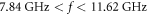 our structure is expected to mimic effectively an interface between positive-ε and negative-ε materials. For example, for the operating frequency
  the effective permittivities are
  and
and  As is well-known, an interface between two media with
  may support SPP waves with a guided propagation constant
  given as [2]:

where  is the free-space wave number and
  is the guided effective refractive index. The guided wavelength is related to the vacuum wavelength as
  The SPP resonance, wherein
  occurs at
  The propagation length of the SPPs can be estimated as
  where
where  is roughly determined from the loss tangent of the dielectric (
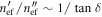 ). In this frequency range the factor
  is at least one order of magnitude larger than in optics. In the appendix, we provide a detailed study of the effect of dielectric and metal loss and demonstrate that it is negligible for microwave designs.
We computed the 'exact' dispersion diagram of the proposed single-interface metamaterial waveguide using the frequency domain solver of CST Microwave Studio® [28] considering a single unit cell of the structure (see figure 1(e)) and Bloch boundary conditions along the x-direction. The dispersion diagram obtained with the CST Microwave Studio® is represented in figure 2(a) with discrete symbols (black circles) and is superimposed on the theoretical result (2) (solid green line). As seen, there is a remarkable agreement between the numerical and analytical results, further validating the theory of [10].

Figure 2. (a), (b) Dispersion diagrams of the single interface SPP modes supported by our plasmonic waveguide-metamaterial (figure 1(a)). Solid green line: analytical result calculated with equation (2). (a) Simulations obtained with the CST Microwave Studio® [28]. Discrete circle symbols: 'exact' dispersion diagram numerically calculated using the Bloch-boundary conditions. Blue dashed curve: dispersion diagram extracted from the phase of the numerically calculated  parameter for a propagating distance
  Dotted black curve: dispersion diagram extracted from the phase of the numerically calculated
  parameter for a propagating distance
  (b) Experimental results obtained from the measured scattering parameters,
  and
and  for a distance between ports,
  and
and  respectively.
Download figure:
Standard image High-resolution imageIn order to determine experimentally the dispersion of the SPPs, the structure was excited by a horizontal dipole with arms aligned along the x-direction. The excitation dipole is either at port 1 or at port 2 of figure 1(d), depending on the measurement. The guided wave is characterized using a similar receiving antenna (port 3) (see figures 1(c) and (d)). The dipole can excite both a space wave and the guided SPP mode, the latter being the main radiation channel. Indeed, the efficiency of the excitation depends on how well the fields generated by the dipole match the profile of a mode. Importantly, the near-field of the dipole is formed by high-frequency spatial harmonics which can strongly couple to the SPP mode due to its intrinsic short wavelengths.
Neglecting the effects of reflections of the SPP wave at the receiving antenna and at the sidewalls (all the lateral walls were covered with microwave absorbers), it follows that the phase  of the transmission coefficient (scattering parameter
  ) from port j to port i is such that
  where l is the distance between the two ports and
  is some reference phase that only depends on the properties of the dipole antennas. Hence, the effective refractive index of the SPP surface wave
  may be obtained from

In practice,  was set equal to
  which corresponds to the phase calculated at the frequency wherein the SPPs start propagating and the amplitude of the signal sensed by the receiving antenna becomes significant. The dispersion diagram measured using this method is depicted in figure 2(b) for the propagating distances
  and
and  As seen, there is a generically good agreement with the effective medium theory result (solid green line), especially for the longer propagating distance. The arms of the transmitting and the receiving dipoles have a finite length along the direction of the SPP propagation. This may cause an integrating effect on the phase of
  and some ambiguity in the definition of l, which is not accounted for in equation (3). Such finite-length 'correction' is less significant for larger values of l, which explains the better agreement in the
  case. For comparison, we also provide in figure 2(a) the dispersion diagram obtained using the CST Microwave Studio® using the same extraction method (blue dashed and black dotted curves), for the same scenario as in the experiment, with the scattering coefficients
  obtained with a full wave numerical simulation. These diagrams have features analogous to the diagrams obtained with the experimental data in figure 2(b).
The electric field profile associated with the SPP waves was calculated using the CST Microwave Studio® (see figure 3) considering the same setup as in the experiment. Time snapshots of the electric field components  and
and  are represented in figures 3(a) and (b), respectively, for three different operating frequencies. As expected from the plasmon features, the surface wave is strongly confined at the interface between the two filling materials. Typical of the SPP propagation, the electric field components
  and
and  decay exponentially in the direction orthogonal to the interface. As expected,
  is flipped across the interface due to the different signs of the effective permittivity (figure 3(b)). Consistent with the dispersion diagram in figure 2, the guided wavelength is shorter for higher frequencies (figures 3(aiii) and (biii)).

Figure 3. Numerically simulated field profiles of the SPPs supported by the waveguide-metamaterial prototype calculated at the mid-plane of the structure and for excitation of port 1. (a) Time snapshot of the transverse electric field component  (ai)
(ai)  (aii)
(aii)  (aiii)
  (b) Similar to (a) but for the normal electric field component
Download figure:
Standard image High-resolution imageThe proposed paradigm enables extending the SPP concept to microwaves and terahertz frequencies and creates the conditions for the design of ultra-compact devices and waveguides. As an example, we consider an edge (Fabry–Pérot type) resonator formed by 34 wires, spanning length  (figure 4(a)). The resonator can be regarded as a truncated SPP waveguide. The resonance condition is given by
  where
where  is the phase of the reflection coefficient of the SPP wave at the ends of the truncated waveguide, and
  labels the resonant mode [29]. Unfortunately,
  is not known analytically but it can be determined based on a numerical simulation. The resonance frequencies can be experimentally characterized by exciting the resonator with a small antenna (in our case the electric dipole located at
  ) and by detecting the dips in the amplitude of the reflection coefficient (
 ). Figure 4(b) shows the plot of
  versus frequency, confirming the presence of several resonances. The difference between the experimental (blue curve) and the CST Microwave Studio® (green curve) results (e.g. the strength of the
  resonance) is mainly due to the fabrication tolerances and the imperfect alignment of the dipole antenna. In addition, the microwave absorbers that surround the prototype are not ideal, and this causes that a few cavity modes (not related to the linear resonator) can be excited as well in the experiment. These cavity modes are usually associated with shallow dips in
  coefficient. Finally, it is important to keep in mind that only a few resonator modes are significantly excited by the antenna due to a mismatch between the field profiles and the antenna near field. The resonances that are better excited in the experiment occur for
  and are labeled with
  in figure 4(b). They match reasonably well the corresponding dips in the CST Microwave Studio® simulation. We numerically verified that these resonances are indeed resonator modes of order m. This is shown in figure 4(c), which represents a time snapshot of the electric field associated with each resonance. As seen, the fields are associated with a standing wave with m lobes (
 zeros). The dispersion diagram obtained with these four resonances (using
  and ignoring the phase
  which is a reasonable approximation for a resonator with a significant number of wires, i.e. with a large L) is shown in figure 4(d). As seen, there is generically a good correspondence between the theoretical model and the experimental results obtained with the resonance frequencies of order m = 4, 5, 6 and 9, where the discrepancy is mainly related to the neglect of

Figure 4. Edge resonator formed by a truncated SPP waveguide. (a) Photograph of the SPP resonator prototype formed by 34 metallic wires. (b) Amplitudes of the simulated and measured scattering parameter  for an excitation (dipole 3) located at
  The resonance frequencies of order m = 4, 5, 6 and 9 are marked in the plot. (c) Numerically simulated time snapshot of the electric field
  for the resonance frequencies of order m = 4, 5, 6 and 9 (the area of the density plot may vary slightly from case to case). (d) Analytical dispersion diagram and experimental dispersion diagram points obtained from the reflection dips of figure 4(b).
Download figure:
Standard image High-resolution image3. Conclusions
In summary, single interface plasmons have been experimentally verified at microwave frequencies through waveguide structures involving only conventional low loss positive-epsilon dielectrics. The metallic wires at the interface of the two dielectric regions guarantee the exclusive propagation of the TE1 mode, and are the key to unlock the plasmonic effects using a waveguide-based metamaterial design. Full-wave numerical simulations and experimental measurements confirm the theoretical foundations of the equivalence between the proposed waveguide-metamaterial structure and an effective positive-ε medium paired with an effective negative-ε medium. Moreover, to illustrate the applications of the proposed paradigm we designed an edge Fabry–Pérot resonator formed by a truncated SPP waveguide. It is envisioned that this paradigm can have potential applications in the realization of microwave and terahertz plasmonic devices with low loss materials, particularly in systems where it is crucial to enhance light–matter interactions in a subwavelength scale. For example, if a subwavelength object is placed in the vicinity of the metamaterial interface, it will scatter strongly the SPP wave because of the short wavelengths of the wave. Thus, the proposed structure may find applications in sensing, spectroscopy, near-field imaging or even in free-electron lasers [30, 31].
Acknowledgments
This work was funded by Fundação para a Ciência e a Tecnologia under project PTDC/EEI-TEL/4543/2014 and by Instituto de Telecomunicações under project UID/EEA/50008/2013. F R Prudêncio acknowledges financial support by Fundação para a Ciência e a Tecnologia (FCT) under the Post-Doctoral fellowship SFRH/BPD/108823/2015. NE acknowledges partial support from the US Air Force Office of Scientific Research (AFOSR) Multidisciplinary University Research Initiatives (MURI) grant number FA9550-14-1-0389.
Appendix
In this appendix, we study the impact of dielectric and metal loss in the propagation constant of the SPPs. To this end, we numerically calculated for a fixed frequency the reflection coefficient R as a function of  when a TE1 waveguide mode illuminates the interface between the two-waveguide regions in figure 1(b). Here,
  is the (real-valued) wave number of the incident wave along x. For sufficiently large values of
  the incident wave is evanescent, i.e., it decays along the y-direction perpendicular to the interface. When the value of
  coincides with the propagation constant of a guided mode (
 ), the incident wave excites a natural mode of the system and in the absence of material loss
  Thus, the guided modes are determined by the poles of
  In the presence of loss, the poles become complex-valued, i.e.,
  is complex-valued. For weak loss, the reflection coefficient near the pole can be approximated by
 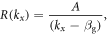 so that

The peak of R is attained at  and the −3 dB bandwidth of the resonance (when the amplitude of R is 70% of the maximum) is
  From here it follows that:

In the above,  (with
(with  ) is the guided effective refractive index, and
  (
( ) is the value of
  greater (less) than
  such that the reflection coefficient
  is 70% of its maximum.
Figures A1(ai) and (aii) show the amplitude of the reflection coefficient  plotted as a function of the normalized wave number of the incident wave,
  for dielectric substrates with


 and
and  for
for  As expected, the quality factor of the resonance decreases as the loss is increased. Figure A1(aiii) shows the calculated
  obtained from the curves depicted in figures A1(ai) and (aii). As seen, for
  the effect of dielectric loss is insignificant. Furthermore, consistent with the theoretical estimate of the main text, the numerical results confirm that for small values of
 is proportional to
  and at the considered frequency the proportionality constant is such that
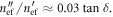

Figure A1. (ai), (aii) Amplitude of the reflection coefficient  as a function of the wave number
  of the incident wave for
  The peaks are associated with the resonant excitation of the guided mode. The attenuation constant of the guided mode is determined by the quality factor of the resonance (−3 dB bandwidth). (aiii) Discrete symbols: calculated values of
  as a function of the loss tangent of the dielectric (the symbols are joined with dotted lines to ease the interpretation of the data).
Download figure:
Standard image High-resolution imageWe made a similar study to investigate the impact of metal loss on  particularly at high frequencies. The methodology is the same as that described previously for the study of the dielectric loss. Figure A2(ai) shows the amplitude of the reflection coefficient
  a function of
  for different values of
 being the conductivity of the metal and
  the vacuum permittivity. We use normalized units so that
 and
and  similar to the design discussed in the main text. For
  with
with  the copper conductivity, the parameters are as in the main text for an operational frequency of 8.4 GHz. The cases
  correspond to designs scaled to the working frequency
  (i = 1, 2, 3), with the metal taken as copper. For simplicity, the metal conductivity is assumed frequency independent. As seen, in figure A2(aii) the proposed structure is fairly robust to the effect of metal loss, even for the designs operating at THz frequencies (i = 2, 3).

Figure A2. (ai) Amplitude of the reflection coefficient  as a function of
  for different values of
  The case
  corresponds to the design of the article with the metal taken as copper and for an operation frequency of 8.4 GHz. (aii) Discrete symbols: calculated values of
  as a function of
  (the symbols are joined with dotted lines ease the interpretation of the data).
Download figure:
Standard image High-resolution image