


Abstract
We investigate the dynamics of the impact ionization (IMI) process in silicon in extremely high fields in the MV/cm range and at low initial carrier concentrations; conditions that are not accessible with conventional transport measurements. We use ultrafast measurements with high-intensity terahertz pulses to show that IMI is significantly more efficient at lower than at higher initial carrier densities. Specifically, in the case of silicon with an intrinsic carrier concentration (∼1010 cm−3), the carrier multiplication process can generate more than 108 electrons from just a single free electron. The photoexcited carrier density dependence of the IMI rate shows that with decreasing initial carrier density the rate increases and approaches the fundamental Okuto limit imposed by energy conservation.
Export citation and abstract BibTeX RIS

Original content from this work may be used under the terms of the Creative Commons Attribution 3.0 licence. Any further distribution of this work must maintain attribution to the author(s) and the title of the work, journal citation and DOI.
Carrier multiplication (CM) through impact ionization (IMI) plays an important role in efficient photovoltaic nano-materials [1, 2], electroluminescent emitters [3], and sensitive photon detectors for optical quantum information applications and biomedical imaging [4]. IMI in extremely high electric fields is also essential to understanding the physics of laser ablation [5] and high harmonic generation [6, 7]. As semiconductor devices shrink to nano-scale dimensions, those with gate voltages of 1 V experience high electric fields beyond 1 MV cm−1. Simultaneously, the cutoff frequencies of modern electronic devices are being pushed into the terahertz (THz) range [8–10]. Under such conditions, carrier-initiated IMI in conjunction with Zener tunneling and intervalley scattering become critical factors affecting nonequilibrium transport phenomena beyond the Boltzmann transport equation. However, the effect of CM on nonlinear transport is not fully understood on femtosecond timescales even though they can no longer be ignored in ultrafast (opto-) electronic devices.
In the presence of a strong electric field, the instantaneous potential energy in a semiconductor can drop significantly over atomic distances, facilitating field-induced interband Zener tunneling [11]. This process can generate a large density of carriers on ultrashort time scales. On the other hand, electrons already in the conduction band can be accelerated by strong electric fields and gain sufficient energy to scatter electrons from the valence band to the conduction band, thereby creating new electrons and holes during the collision [12]. This IMI process continues in a cascaded manner such that significant quantities of free charge carriers may be generated. The two carrier generation mechanisms occur on the femtosecond time scale, and in many cases, it is difficult to identify the dominant carrier generation mechanism in a definitive manner.
Here, we investigate the CM mechanism in the ubiquitous semiconductor silicon (Si) in the presence of an intense THz field. So far, experimental studies on IMI have mainly been based on transport measurements made on doped p–n junction Si devices with a quasistatic electric field bias [13–15]. Ultrafast optical pump-probe studies of IMI in a different material system (GaAs p–i–n heterostructure) has been performed [16], with spatiotemporal dynamics of the IMI process studied at low (10 K) temperature, using external fields below the static breakdown limit of 450 kV cm−1, and with the initial carrier concentration defined by optical excitation. Thus, previous investigations have been limited to using electric field strengths in the sub-MV/cm range because of problems of overheating and avalanche breakdown, and at high initial carrier concentrations in order to drive a measurable current across the junction. The effects of heating can be significantly reduced by using ultrashort electric field pulses. Recently, the advent of intense THz pulses has enabled investigation of IMI by purely using optical methods [17–19]. In particular, a combination of an intense THz field and local field enhancement by metallic dipole antennas [20–23] enabled us to achieve electric fields of several MV/cm. Moreover, optical doping of the semiconductor allows us to investigate the CM dynamics over a wide range of initial carrier concentrations.
In the experimental setup shown in figure 1(a), an intense THz field is incident from the substrate side of a high resistivity silicon (100) substrate (intrinsic carrier density of 1.5 × 1010 cm−3) with a 200 nm thick gold antenna array fabricated on its surface. The THz pulses are generated by optical rectification of femtosecond pulses from a Ti:sapphire laser amplifier (repetition rate: 1 kHz, central wavelength: 800 nm, pulse duration: 100 fs, and pulse energy: 4 mJ) in a LiNbO3 crystal using the tilted-pulse-front scheme [24, 25]. The THz beam is focused on the sample by using an off-axis parabolic mirror with a 50 mm focal length. The maximum electric field strength of the incident THz pulse is set to be 0.5 MV cm−1 and the field strength is varied by changing the relative angle between two crossed wire-grid polarizers. A full-wave electromagnetic (FWE) simulation shows that metallic dipole antennas in an array configuration [26] enhance the peak electric field in the vicinity of the antenna tips, leading to a maximum peak electric field of 3.6 MV cm−1 inside silicon at a distance of 1 μm from the metal tip. The simulated local electric field enhancement profile is shown in figure 1(c).

Figure 1. (a) Schematic diagram of the pump-probe setup used to investigate THz-induced IMI in silicon. A CCD image of unit cell of the antenna array with bright probe spot (dashed circle) is shown in the inset. (b) Calculated local electric field enhancement profile near the antenna tip. (c) Carrier transitions in Si band structure: interband transitions due to optical pump (1), L-to-X intervalley scattering (2) and carrier multiplication through IMI (3), phonon-assisted interband transition (4). The band structure is adapted from [27].
Download figure:
Standard image High-resolution imageThe temporal evolution of the carrier density is probed quantitatively by measuring the transient reflectivity change at normal incidence of a weak near-infrared (NIR) pulse tightly focused on the sample to a diameter of approximately 2 μm (see the inset of figure 1(a)). An optical near-UV (NUV) pre-pump pulse at 400 nm generates a controlled concentration of free carriers before the arrival of the THz pulse. The NUV pulse is generated by frequency doubling in a nonlinear beta barium borate crystal and it is focused on the sample to a diameter of approximately 50 μm. The large cross-sectional area compared with the probe spot size minimizes carrier ambipolar diffusion parallel to the sample surface on the probe signal.
Possible transitions of carriers in the presence of NUV and THz excitations in respective temporal order are depicted in figure 1(b). The photon energy of the NUV pump pulse (3.1 eV) is close to the bandgap near the L symmetry point (the smallest direct band gap), so interband transitions (process 1) result in electrons in the L-valley. Then electrons undergo L–X intervalley scattering (process 2) with a time constant of 180 fs [28]. The electron distribution is thermally equilibrated with the lattice via phonon scattering within less than 2 ps [28–30]. The THz electric field is parallel to the (110) direction and accelerates conduction band electrons. Collisions of energized electrons with valence band electrons results in new electron–hole pairs (process 3)—IMI. In accordance with energy and momentum conservation, the IMI process in Si is possible only if the electron has a threshold kinetic energy higher than the band gap of Si [12]. The phonon-assisted interband transition due to the probe pulse is shown as process 4 in the figure.
The relative NIR reflectivity changes  for several strengths of electric field are shown in figure 2 for initial carrier densities (Ni) of 1.5 × 10¹⁰, 1.3 × 10¹⁹, and 9.5 × 1019 cm−3. In figure 2(a) the optical NUV pump is blocked and the initial carrier density is equal to the intrinsic carrier density of the silicon substrate. The first drops in reflectivity near t = −7 ps in figures 2(b) and (c) are caused by the NUV pre-pump excitation and the reflectivity changes can be mainly attributed to the free carrier response through the following relationship [31],

where ΔN is the change in charge carrier density, e is the electronic charge, ω is the probe angular frequency, is the dielectric permittivity of the vacuum, m* = 0.156me (me is the electronic mass) is the effective optical mass of carriers [30], and
  = 3.68 is the refractive index of silicon with the intrinsic carrier concentration at probe frequency [31]. The second drops in reflectivity near t = 0 ps overlap with the THz pulse, showing that the THz pulses cause additional carrier generation. The reflectivity drops show fast recovery within a few picoseconds because of nonradiative relaxation processes including Auger recombination [32, 33].
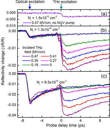
Figure 2. NIR reflectivity change with an initial optical excitation followed by THz excitation at various incident field strengths for initial carrier densities of (a) 1.5 × 10¹⁰, (b) 1.3 × 10¹⁹, and (c) 9.5 × 1019 cm−3. Color-coding of the THz field strength is the same for (b) and (c). The initial density of carriers is varied by changing the incident NUV pump power using optical density filters and the THz field strength is varied by tuning the relative angle between the two crossed wire-grid polarizers.
Download figure:
Standard image High-resolution imageIn the case of the intrinsic initial carrier concentration without NUV excitation (figure 2(a)), a salient drop in reflectivity occurs after THz pulse excitation and the maximum ΔR/R ≈ 2.5 × 10⁻³ is the same order as that obtained for the optical excitation with 1019 cm−3. In addition, figures 2(b) and (c) show that the reflectivity changes are amplified by THz excitation, and also that the relative increment of carrier density caused by the THz excitation depends strongly on the initial carrier density. These results indicate that the THz excitation enables the carrier density to be increased by more than eight orders of magnitude through IMI processes rather than through Zener tunneling, which is not facilitated by the carrier doping.
A simplified Monte Carlo (MC) was performed in order to ascertain the mechanism of the carrier generation and amplification caused by the THz excitation. In the MC, an electron propagates in a linearly polarized THz field that has a temporal profile of a measured THz transient. The temporal evolutions of the electron energy  and carrier density
  in the THz field are calculated considering the effective conductivity mass of the electron in its acceleration. The MC simulation considers IMI to be one of the scattering mechanisms. The total scattering rate is given by
 where
where  is the energy-dependent phonon scattering rate [34],
  is the carrier density-dependent electron–hole scattering rate [35], and
  is the electron energy-dependent IMI rate [36]. The carrier density is calculated as
 where
where  is a stochastic parameter that has a value of 2 if IMI happens and 1 otherwise.
  is the sum of the direct and indirect band-to-band tunneling rates [37] and the Auger recombination rate is given by
  where
where  = (2.8, 0.99) × 10−31 cm6 s–1 are the Auger coefficients for e–e–h and e–h–h processes, respectively [38].
Figure 3(a) shows the reflectivity changes obtained from equation (1) and the MC simulation, and from the measurement for Ni = 1.3 × 1019 cm−3 and full THz illumination. Figures 3(b) and (c) compare the CM factors, i.e. the ratio of carrier densities after and before the THz excitation, between the experiment and calculation. The figures show that the simplified MC simulation7 reproduces the field and initial carrier density dependences of the CM factor. The good agreement indicates that the carrier generation happens within the sub-picosecond duration of the THz pulse through the IMI process.
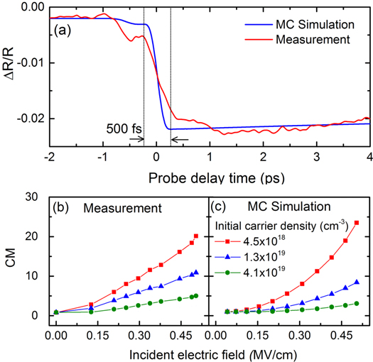
Figure 3. (a) Comparison of the dynamics of reflectivity change between the calculation (obtained by equation (1) and MC simulation) and measurement for Ni = 1.3 × 1019 cm−3. (b) Measurement and (c) simulation of the carrier multiplication factor as a function of the incident electric field for three initial carrier densities.
Download figure:
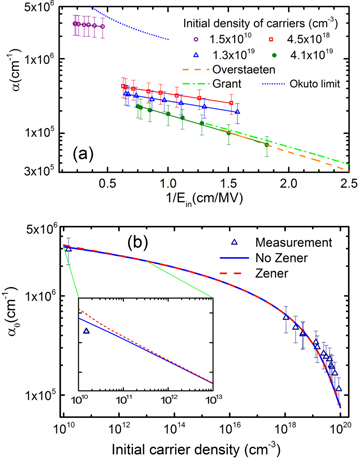
Standard image High-resolution imageTo clarify the differences between IMI processes observed by our technique and the conventional direct current (DC) transport measurement technique, the IMI coefficient  is calculated from the CM factor, which is defined as the number of IMI events per unit length, is calculated as a function of the electric field from the CM factor:
  [13]. Here,
  is the duration of the THz-induced reflectivity drop and the calculations assume a constant drift velocity,
  of 1.0 × 107 cm s−1 [34, 39]. The measured
  versus
  is shown in figure 4(a) together with commonly cited experimental data, obtained by measurement of DC amplification in p–n junction devices [13, 14]. Even though the measurement methods and types of excitation are different, the field dependence of IMI for the optically pumped samples agrees very well with the previous measurements, especially for the highest initial carrier density. The previously used p–n junction diodes had highly doped IMI regions with comparable initial carrier densities set by our optical excitation. The
  versus
  plot was represented by a linear fit showing that the exponential model of the IMI field dependence due to Chynoweth [15] can describe the IMI process with ultrashort electric field pulses with peak fields in the MV/cm regime.
Figure 4. (a) IMI coefficient for different carrier densities as a function of inverse of peak electric field Ein with linear fits (measurement); dashed and dash-dot curves are experimental results from literature [13, 14]. The dotted line is a theoretical limit based on conservation of energy. (b) IMI coefficient as a function of initial carrier density determined from measurements (triangle symbols) and MC simulations (lines) for the highest incident THz illumination. The red dashed and blue solid lines are simulation results with and without the contribution of Zener tunneling respectively.
Download figure:
Standard image High-resolution image
The experimentally obtained IMI coefficient of up to 3 × 106 cm−1 (purple open circles in figure 4(a)) approaches the fundamental Okuto limit imposed by energy conservation (blue dotted curve figure 4(a)) [40]. The Okuto limit is based on the assumption that all the energy lost from the THz field is used for the IMI process. Considering IMI by both electrons and holes, the limiting IMI coefficient can be written as  where
where  is the bandgap energy of silicon. Such a high IMI coefficient at low initial carrier density is more than one order of magnitude larger than the extrapolations made from the previously reported values (the orange and green dashed and dash-dotted curves, respectively, in figure 4(b)) [18, 19]. At the intrinsic initial carrier density, only a single electron on average is found in the high field region near the antenna tips (7 × 3 × 2 μm3, defined loosely by a 1 μm wide and 2 μm deep band surrounding the 5 μm wide antenna tip). Therefore, from the observed reflectivity change (figure 2(a)), a population of 9.3 × 10⁸ free electrons is generated within a few hundred fs in the highest field of our experiments, and this corresponds to an ultrafast cascade of 30 IMI events, causing to the amplification of ΔN by 230 ≈ 109.
Figure 4(b) shows the dependence of the IMI coefficient on the initial carrier density at a fixed incident THz field of 0.5 MV cm−1. Here, the measurement and simulation show that IMI coefficient decreases with increasing initial carrier density. At high carrier densities (the final density is on the order of 1020 cm−3), Auger recombination competes with IMI by effectively depleting carriers [38], and e–h scattering reduces the energy gain of the electrons in the conduction band [35]. In addition, field screening by free carriers reduces the local electric field inside the silicon substrate, which in turn reduces the IMI coefficient. Consideration of these effects in the MC simulation reproduces the measured IMI coefficient across more than 9 decades of initial carrier densities. Figure 4(b) also shows that the contribution of Zener tunneling is too small to affect the IMI coefficient. The large direct bandgap of silicon (∼3.4 eV at  point) requires a very strong electric field to lower the potential energy sufficiently for valence band electrons to tunnel into the conduction band [41], and the tunneling rate is much smaller than the IMI rate.
In conclusion, we have shown that ultrashort THz pulses enable experimental investigation of IMI dynamics in Si over a broad, nine decades wide, initial carrier density range in the multi-MV/cm electric field regime, which had been inaccessible up until now because of the problem of avalanche breakdown. Even though the applied electric field significantly exceeded the damage threshold for DC fields, the Chynoweth IMI model is valid in the MV/cm regime. At the lower limit of the initial carrier density (1.5 × 1010 cm−3) the IMI coefficient approaches the fundamental Okuto limit imposed by energy conservation. We found that at this limit, a single electron initially present within the experimental volume can be multiplied to more than 108 electrons within a few hundred fs. Consequently, by controlling the presence of a single electron, the whole CM process can be switched on and off. These results pave the way to a new interface between single-electron nano-electronics and macro-scale electronics operating at ultrahigh speeds.
Acknowledgments
The authors acknowledge travel support from the Scandinavia-Japan Sasakawa Foundation, support from the Danish Council for Independent Research (DFF project THz-GUN, No. 64092), and support by KAKENHI (26286061, 17H06124) from JSPS.
Footnotes
- 7
The adjustment factor of the electric field is a fitting parameter to make the CM in the simulations (figure 3(c)) fit the measurements (figure 3(b)) for each initial carrier density. The electric fields calculated in the FWE simulation (figure 1(b)) have to be enlarged to match the experimentally obtained CM and the factors randomly range from 1.2–2.5. The adjustment factors might come from the uncertainties in the probe location and defects in the shape of antenna.