
Abstract
An analog-assisted digital low dropout regulator (AAD-LDO) is proposed to solve the problems of a slow transient response and a large output ripple in a conventional digital LDO. In the AAD-LDO, a fast-response auxiliary analog LDO is added to the digital LDO in parallel. Compared with the digital LDO, the measured AAD-LDO in 180 nm CMOS reduces the transient response time and the output ripple by 59 and 28%, respectively, at the same current efficiency of 97.1%. The line regulation is 15 mV/V and the load regulation is 0.63 mV/mA.
Export citation and abstract BibTeX RIS
1. Introduction
The number of on-chip voltage converters is increasing, because recent SoC's require a lot of power supply voltage. A low dropout regulator (LDO) is a reasonable choice for the on-chip voltage converters, because LDO requires no off-chip components. The low-power SoC's require a low-input-voltage LDO with the low quiescent current (IQ) (= supply current for a controller in LDO).1–23) A digital LDO1–5,24,25) achieves the low-input-voltage operation with a low IQ. The problems of the digital LDO, however, are a slow transient response and a large output ripple. To solve these problems, an analog-assisted digital low dropout regulator (AAD-LDO) is proposed.
2. Problems of conventional LDOs
Figure 1 shows a conventional analog LDO. The current efficiency (η) of the analog LDO is low owing to the high IQ in the operational amplifier. Figure 2 shows a conventional digital LDO.1) In the digital LDO, the current efficiency is high owing to the low IQ in the controller and the comparator, though the transient response is slow and the output ripple is large. In order to reduce the transient response time, a high-frequency clock (Clk) is required, which increases IQ and decreases η.2,3) In order to reduce the ripple, the unit gate width (WUNIT) of the power transistors is reduced and the number (n) of power transistors is increased. The increased n, however, increases IQ and decreases η. Therefore, a new circuit is required to reduce both the transient response time and the ripple without decreasing η.
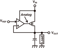
Fig. 1. Conventional analog LDO.
Download figure:
Standard image High-resolution image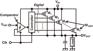
Fig. 2. Conventional digital LDO.1)
Download figure:
Standard image High-resolution image3. Proposed analog-assisted digital LDO
Figure 3 shows the concept of the proposed AAD-LDO. In the AAD-LDO, a fast-response auxiliary analog LDO is added to the digital LDO in parallel. Figure 4 shows a detailed schematic of the proposed AAD-LDO. In the AAD-LDO, the digital LDO is the main LDO and the analog LDO is auxiliary LDO, because WANALOG < WDIGITAL. The digital LDO slowly controls the output voltage (VOUT) with a coarse digital voltage step. In contrast, the analog LDO quickly controls VOUT with a fine analog voltage control. By operating both the digital LDO and the analog LDO simultaneously in parallel, the AAD-LDO reduces both the transient response time and the output ripple.
Fig. 3. Concept of proposed AAD-LDO.
Download figure:
Standard image High-resolution image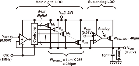
Fig. 4. Detailed schematic of proposed AAD-LDO.
Download figure:
Standard image High-resolution image4. Measurement results and discussion
Both the AAD-LDO and the digital LDO are fabricated in 180 nm CMOS. In the AAD-LDO and the digital LDO, the digital LDO part is the same and only the AAD-LDO has the analog LDO. Figure 5 shows the chip photomicrograph and the layout of the AAD-LDO. The total chip area was 1.2 × 0.5 mm2. The core areas of the digital and analog LDOs are 200 × 170 µm2 and 30 × 50 µm2, respectively.
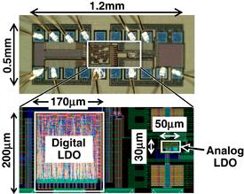
Fig. 5. Chip photomicrograph and layout of AAD-LDO.
Download figure:
Standard image High-resolution imageTable I shows a measured performance summary of the AAD-LDO. The fabricated AADLDO achieved the 1.2 V input voltage and 0.95 V output voltage with 99.6% current efficiency and a 14.2 µA quiescent current at a 3.4 mA load current (IOUT). The static line regulation is 15 mV/V when the input voltage (VIN) is varied from 1.15 to 1.25 V. The static load regulation is 0.63 mV/mA when IOUT is varied from 1.7 to 3.4 mA.
Table I. Performance summary of AAD-LDO.
| CMOS technology | 180 nm |
| Active area | 0.036 mm2 |
| Clock frequency | 1 MHz |
| Input voltage | 1.2 V |
| Output voltage | 0.95 V |
| Maximum load current | 11 mA |
| Nominal load current (l1) | 3.4 mA |
| Output capacitor | 10 nF (Off-chip) |
| Quiescent current at l1 | 14.2–242 µA |
| Current efficiency at l1 | 93.3–99.6% |
| Line regulation | 15 mV/V |
| Load regulation | 0.65 mV/mA |
In the following measurement, VIN is 1.2 V, VOUT is 0.95 V, and IOUT is 3.4 mA. The reference voltage (VREF) is changed from 0.8 to 0.95 V and the response time of VOUT is measured at the load resistance of 270 Ω.
In the design of the LDO, η, the transient response time of VOUT, and the ripple of VOUT are three important characteristics. In the conventional digital LDO, the clock frequency is a key parameter to tune the characteristics. In contrast, in the proposed AAD-LDO, both the clock frequency and the bias current of the operational amplifier in the analog LDO are key parameters to tune the characteristics.
In order to find the optimum clock frequency in the AAD-LDO, Fig. 6 shows the measured η dependence of the transient response time in the AAD-LDO. Both the clock frequency and the bias current are varied. When the clock frequency is increased from 200 kHz to 4 MHz, both the transient response time and η are reduced. In this work, the clock frequency of 1 MHz is used in the following measurement to achieve η larger than 98% and a fast transient response time.
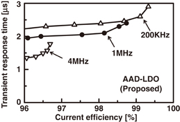
Fig. 6. Measured η dependence of transient response time in AAD-LDO.
Download figure:
Standard image High-resolution imageFigures 7 and 8 show the measured η dependence of the transient response time and the peak-to-peak ripple of VOUT, respectively, in the conventional digital LDO and the proposed AAD-LDO. The clock frequency is varied from 1 to 14 MHz in the digital LDO, while the bias current of the operational amplifier is varied from 1 to 15 µA in the AAD-LDO at the clock frequency of 1 MHz. Compared with the conventional digital LDO, the proposed AAD-LDO reduces the response time from 40 to 2.4 µs by 94% and from 4.4 to 1.8 µs by 59% at η of 99.6 and 97.1%, respectively. Figure 9 shows the measured waveforms of VREF and VOUT at η of 99.6%. Similarly, AAD-LDO reduces the ripple from 10.8 to 7.8 mV by 28% at η of 97.1%, as shown in Fig. 10.
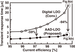
Fig. 7. Measured transient response time vs current efficiency.
Download figure:
Standard image High-resolution image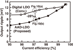
Fig. 8. Measured output ripple vs current efficiency.
Download figure:
Standard image High-resolution image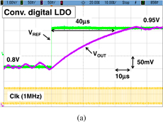
Download figure:
Standard image High-resolution image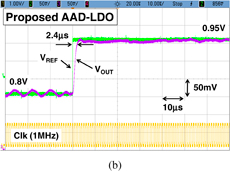
Fig. 9. Measured transient waveforms of VREF and VOUT at η of 99.6%. (a) Conventional digital LDO. (b) Proposed AAD-LDO.
Download figure:
Standard image High-resolution image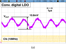
Download figure:
Standard image High-resolution image
Fig. 10. Measured output ripple waveforms at η of 97.1%. (a) Conventional digital LDO. (b) Proposed AAD-LDO.
Download figure:
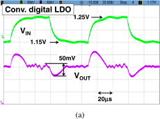
Standard image High-resolution imageIn order to investigate the dynamic line regulation, Fig. 11 shows the measured waveforms of VIN and VOUT of the conventional digital LDO and the proposed AAD-LDO at η of 99.6%. The clock frequency is 1 MHz. VIN is changed between 1.15 and 1.25 V at 10 kHz. In the digital LDO in Fig. 11(a), the transient drop of VOUT at the falling edge of VIN is 50 mV. In contrast, in AAD-LDO in Fig. 11(b), the transient drop is reduced to 5 mV by adding the fast-response auxiliary analog LDO.
Download figure:
Standard image High-resolution image
Fig. 11. Measured waveforms of VIN and VOUT. (a) Conventional digital LDO. (b) Proposed AAD-LDO.
Download figure:
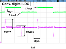
Standard image High-resolution imageIn order to investigate the dynamic load regulation, Fig. 12 shows the measured waveforms of IOUT and VOUT of the conventional digital LDO and the proposed AAD-LDO at η of 97.1%. The clock frequencies of the digital LDO and AAD-LDO are 10 and 1 MHz, respectively. IOUT is changed between 1.7 and 3.4 mA at 10 kHz. In the digital LDO in Fig. 12(a), the transient drop of VOUT is 100 mV. In contrast, in the AAD-LDO in Fig. 12(b), the transient drop is reduced to 40 mV by adding the fast-response auxiliary analog LDO.
Download figure:
Standard image High-resolution image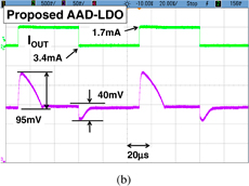
Fig. 12. Measured waveforms of IOUT and VOUT. (a) Conventional digital LDO. (b) Proposed AAD-LDO.
Download figure:
Standard image High-resolution image
5. Conclusions
The AAD-LDO is proposed to solve the problems of the slow transient response and the large output ripple in a conventional digital LDO. Compared with the digital LDO, the measured AAD-LDO in 180 nm CMOS reduces the transient response time and the output ripple by 59 and 28%, respectively, at the same current efficiency of 97.1%. At the dynamic change of VIN, the transient drop of VOUT is reduced from 50 to 5 mV by adding the fast-response auxiliary analog LDO in the AAD-LDO. Similarly, at the dynamic change of IOUT, the transient drop of VOUT is reduced from 100 to 40 mV in the AAD-LDO.
Acknowledgements
This work was partly carried out as a part of the Extremely Low Power (ELP) project supported by the Ministry of Economy, Trade and Industry (METI) and the New Energy and Industrial Technology Development Organization (NEDO). The VLSI chips were fabricated in the chip fabrication program of VDEC in collaboration with Rohm Co., Ltd. and Toppan Printing Co., Ltd.