
Abstract
This paper presents an ultra-low power low-dropout (LDO) linear regulator with a load current tracking bias current generator (BCG). The proposed LDO employs the load current tracking BCG to achieve stable and ultra-low power operation. The measurement results demonstrated that the proposed LDO produced a 1.2 V output and achieved 78 nA quiescent current, 145 mV mA−1 load regulation, and 2.2 mV V−1 line regulation.
Export citation and abstract BibTeX RIS
1. Introduction
Internet-of-things (IoT) devices need to be small, low-cost, maintenance-free, and ultra-low power. 1–11) Energy harvesting has attracted attention as an alternative power source of batteries. 12–24) However, the output voltage and power of small energy harvesters are basically weak and easily lost, while the operating voltage of IoT devices will be 1.2 V or higher and the current consumption in IoT devices will be in the ranges from several nA to several hundred μA. 2) Thus, a power management system (PMS) is necessary for stable and sustainable operation. Figure 1 shows a block diagram of the PMS. The PMS consists of a voltage boost converter, voltage buck converter, regulators, and energy storage/buffer device. The voltage boost converter converts a low voltage input of the harvester into a high output voltage, and stores the generated voltage on the energy storage device, in case that the harvester cannot generate the electric power steadily. When the application circuits need to operate, the voltage buck converter converts the stored voltage into a lower voltage and then the low-dropout regulators (LDOs) generate stable and appropriate voltages for the application circuits because the output of the buck converter contains a ripple voltage.

Fig. 1. Block diagram of PMS and target of this work.
Download figure:
Standard image High-resolution imageTo realize ultra-low power LDOs, one effective and direct way to save the power consumption is to reduce a bias current of an error amplifier (EA) used in the LDO. Although the LDO can be made low power, there is a stability problem. The stability of the LDO depends on the poles that rotate the phase of the signal. The dominant and non-dominant poles depend on the load current IL and bias current IBIAS, respectively, and are expressed as


In low power LDOs biased with the low bias current, the dominant pole moves toward higher frequency region as the load current IL increases. The dominant pole moves closer to the non-dominant pole. As a result, the phase margin of the LDO decreases and the stability of the LDO degrades.
To solve the problem, LDOs with an adaptive biasing technique have been proposed. 25–30) The technique is used to change the bias current for the EA in accordance with the load current IL. This enables us to change both poles in the same frequency direction in accordance with the load current IL. Thus, the LDOs achieve ultra-low power and wide-load range operation. In our previous work, an LDO using an adaptive biasing circuit consisting of a positive feedback circuit was presented. 25) However, the LDO has two problems; (1) it is difficult to design the amount of adaptive bias current and (2) it generates an undesirable large current before the regulator settles in steady state condition (e.g. start-up condition). 25) In addition, other conventional LDOs using an adaptive biasing technique require a constant current reference circuit or an external current source because they are based on a hybrid architecture of using a constant current source and an adaptive bias current source. 26–29)
In light of this background, we propose an ultra-low power LDO that solves these issues in the previous LDO. The proposed LDO employs a load current tracking bias current generator (BCG) to achieve stable and ultra-low power operation. The BCG generates a bias current in accordance with the load current. It helps maintain the stability in a wide load range. In contrast to our previous work, 31) here, we discuss the issues of the LDO in detail, and then discuss and analyze our proposed circuit operation and its effectiveness.
2. Previous LDO regulator
Here, we briefly summarize the operation of our previous LDO and discuss its issues. Figure 2 shows a schematic of our previous LDO using an adaptive bias technique. 25) The LDO consists of an EA, current feedback circuit (CFC), and output stage. The aspect ratios of the nMOS (MN2: MN3) and pMOS transistors (MP3: MP4: MP5 are set to 1: 2 and 1: 1: α, respectively. With the circuit, the EA and CFC form a positive feedback loop and monitor the load current IL . The operation of the LDO is as follows.

Fig. 2. Schematic of conventional LDO regulator.
Download figure:
Standard image High-resolution imageWhen the IL becomes large, the output voltage VOUT and feedback voltage VFB decrease. The transistor MP2 detects the VFB change, and therefore, I2 and I3 increases. The IOUT also increases because the MP5 monitor the current in the feedback loop. Then the VOUT and VFB increase to maintain VFB = VREF. Therefore, when the load current IL changes, the bias currents in the LDO adaptively change to maintain VFB = VREF. The technique improves the stability of the LDO because two poles move together according to the IL.
However, the LDO has two issues. On the one hand, the adaptive bias current cannot be designed theoretically. This is because current flowing in the circuit is determined by the balance of the positive and negative feedback loops. When the EA detects the output voltage change through VFB (i.e. VFB ≠ VREF), current flowing in MP2 increases by the positive feedback loop. After that, current decreases by the negative feedback loop because VFB increases to VREF (i.e. VFB = VREF). As can be seen by the current generation mechanism, it is difficult to design the amount of the adaptive bias current. On the other hand, the LDO generates undesirable large current before operation. This is because the positive feedback loop operates before the negative feedback loop has been established. As mentioned above, the LDO has two feedback loops and then undesirable large bias current is generated when the negative feedback loop does not work correctly. As discussed in the previous work,
25) when the supply voltage VDD is lower than the desired output voltage, or  , undesirable large current flows in the circuit.
3. Proposed LDO regulator
To solve these issues in the previous LDO, we develop an LDO without the positive feedback loop. Figure 3 shows a schematic of our proposed LDO. The proposed LDO consists of a BCG, differential amplifier, and output stage. The proposed LDO does not use an external current source to bias the differential amplifier. Instead, the BCG with a pass transistor MP7 in the output stage generates the bias current IBIAS. The conventional five-transistor (5T) differential amplifier in the BCG and MN7 are used to set the drain voltage of MP8 equal to the VOUT. This improves the accuracy of pMOS current mirror (MP7: MP8). By setting the aspect ratios of the pMOS transistors (MP7: MP8) and nMOS transistors (MN8: MN9: MN10) to α1:1 and α2:1:1, the IBIAS can be expressed as

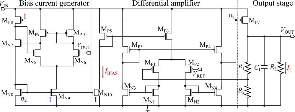
Fig. 3. Schematic of proposed LDO regulator.
Download figure:
Standard image High-resolution imageTherefore, the proposed LDO can be developed without the positive feedback loop, and achieves low power consumption and stable operation because the IBIAS changes in accordance with IL.
4. Results
We evaluated the stability of the proposed LDO using SPICE with a set of 0.18 μm CMOS process parameters. In the proposed LDO, we set VREF, CL, α1, and α2 to 0.6 V, 1.0 μF, 20, and 5, respectively. We used a 1.0 μF off-chip capacitor to keep a phase margin of the LDO, 60 degrees or more. We consider that a few μF capacitor is acceptable if we use an external capacitor. The ratio of the resistors (R1 and R2) was set to 1:1 (i.e. VOUT = 1.2 V). The load resistance RL was set to 50 kΩ and 5 MΩ in the simulation. Figure 4 shows a simulated bode plots. When the load resistance RL was reduced by a factor of 100, from 5 MΩ to 50 kΩ, the pole changed approximately 100 times larger. In both cases, phase margins of 45 degrees or more were achieved. We confirmed that the proposed circuit operates stably even when the RL changes.

Fig. 4. Simulated bode plot.
Download figure:
Standard image High-resolution imageA prototype chip was fabricated using the same CMOS process technology as the simulation. Figure 5 shows the chip micrograph of the proposed LDO. The chip area was 0.013 mm2. Figure 6 shows the measured load transient response when CL and RL were set to 1 μF and 20 kΩ, respectively. We dynamically changed the load current IL by turning on and off an external discrete MOS transistor (ALD1105). The output voltage change was within 9 mV when the IL changed from 0 to 60 μA with a rise/fall time of 1 μs. The proposed LDO can produce a regulated output with low ripple voltage. Figure 7 shows the measured output voltage VOUT as a function of input voltage VIN under no load condition in 10 test chips. The VOUT settled to 1.2 V when the VIN was higher than 1.23 V. The line regulation was 2.2 mV V−1 in the input voltage VIN range from 1.23 to 1.8 V. Figure 8 shows the measured input current IIN as a function of input voltage VIN under no load condition in 10 test chips. During startup, the undesirable large current that occurred in our previous LDO was not generated, and the IIN settled to 78 nA in a steady state. Therefore, the proposed LDO has achieved high accuracy and ultra-low power operation in the quiescent state. Figure 9 shows the measured load regulation in 10 test chips when the input voltage was set to 1.5 V. The load regulation and the maximum load current were 145 mV mA−1 and 0.12 mA, respectively. The load regulation was poor than expected. This was because we designed the pass transistor (MP7) relatively small, i.e. in this work, we used the pass transistor whose channel width and length were 20 and 3 μm, respectively. We think that the maximum load current and the load regulation can be improved by increasing the aspect ratio of the pass transistor (e.g. in the simulation, when we use a pass transistor whose channel width and length are 62.5 and 0.5 μm, the load regulation and the maximum load current can be increased to 5.5 mV mA−1 and 1.5 mA, respectively). Figure 10 shows the measured bias current IBIAS as a function of IL in 10 test chips. We confirmed that the IBIAS can be generated accordingly when the load current changed from 0.12 to 24 μA. The IBIAS can be modeled as

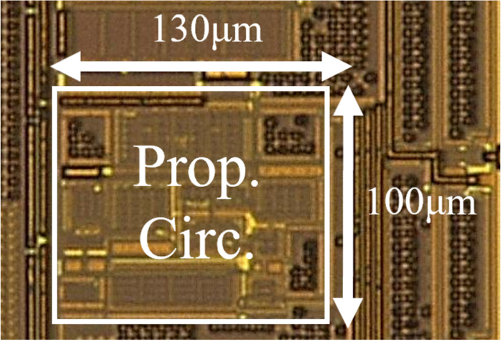
Fig. 5. Chip microgragh of the proposed circuit.
Download figure:
Standard image High-resolution image
Fig. 6. Measured transient waveform.
Download figure:
Standard image High-resolution image
Fig. 7. Measured output voltage as a function of VIN.
Download figure:
Standard image High-resolution image
Fig. 8. Measured input current as a function of VIN.
Download figure:
Standard image High-resolution image
Fig. 9. Measured output voltage as a function of IL.
Download figure:
Standard image High-resolution image
Fig. 10. Measured bias current as a function of IL.
Download figure:
Standard image High-resolution image
The IBIAS saturated above 24 μA because the output voltage of the amplifier in the BCG has reached its upper limit and cannot provide sufficient gate-source voltage to MN7.
Table I summarizes the performance of the proposed LDO in comparison with the prior LDOs using adaptive biasing techniques. 27,28) can supply wide load current up to 10 mA. However, they require additional constant current sources. Compared with Ref. 25, our proposed LDO achieved lower quiescent current. Therefore, our proposed LDO is useful for low-power IoT devices.
Table I. Performance summary and comparison.
| Reference | This work | Ozaki 25) | Huang 28) | Adorni 27) |
|---|---|---|---|---|
| Year | 2023 | 2016 | 2018 | 2020 |
| Technology (nm) | 180 | 180 | 65 | 55 |
| Chip area (mm2) | 0.013 | 0.13 | 0.0048 | 0.042 |
| Constant current source | No | No | Yes | Yes |
| Input voltage VIN (V) | 1.23–1.8 | 4.25–5.0 | 1.0* | 0.8− |
| Output voltage VOUT (V) | 1.2 | 4.2 | 0.8 | 0.6 |
| Load capacitor CL (nF) | 1000 | 10000 | 0.01 | 1000 |
| Max load current IL (mA) | 0.12 | 1-6.8 | 10 | 10 |
| Quiescent current (μA) | 0.078 | 0.151 | 0.1 | 0.016 |
| Line regulation (mV V−1) | 2.2 | 5.0* | N/A | 0.5 |
| Load regulation (mV mA−1) | 145 | N/A | 1.58 | 1.05 |
| Voltage droop (mV) | 9 | N/A | 231.4 | 70 |
| ΔIL (mA) | 0.06 | N/A | 10* | 10 |
*Estimated from figure.
5. Conclusion
We proposed an ultra-low power LDO with a load current tracking BCG. The bias current of the LDO can be changed in accordance with the load current. This solves the issues of the conventional LDO and enables stable and ultra-low power operation to be achieved. The measurement results demonstrated that the proposed LDO achieved a 1.2 V output, 78 nA quiescent current, 145 mV mA−1 load regulation, and 2.2 mV V−1 line regulation.
Acknowledgments
This work was supported through the activities of VDEC, the University of Tokyo, in collaboration with Cadence Design Systems and Mentor Graphics. This work was also partly supported by JSPS KAKENHI Grant No. 20H00606, 22H03558, and 23H03364.