
Abstract
The design proposes a low-dropout regulator incorporating dynamic loop gain control to accommodate a wide load current range. It introduces a multi-phase error detection mechanism, a tri-state damping selector, and a dynamic integration shift register. These elements predict load variations and dynamically increase loop gain when the load variation is significant, all without increasing the input clock. This approach achieves a fast response and low power consumption simultaneously. The chip was implemented in 0.18 μm CMOS, with an input operating voltage of 1.2 V and an output voltage of 1 V. The measured results revealed that it could provide output currents from 0.5 to 150 mA, indicating that it had a 300 times wider current range. The maximum current efficiency was 99.93%, and the core area was 0.198 mm2.
Export citation and abstract BibTeX RIS
1. Introduction
As electronic products continue to flourish, chips are striving for high performance while ensuring low power consumption. However, fluctuations in power consumption cause the current to fluctuate, making it crucial to provide stable power under wide-ranging load changes for power management chips. Digital low-dropout regulators (LDOs) 1–4) offer advantages over analog LDOs, 5–10) such as lower static power consumption, smaller size, and better transient response, despite potential output ripple and poor noise immunity. However, when facing larger load variations, digital LDOs can easily generate spike voltages and even experience significant momentary voltage dropouts during the transition from light to heavy loads, resulting in adverse effects on load circuits. Traditional digital LDOs typically increase the circuit clock or loop integral to achieve a faster transient response, 11–14) but this can lead to larger output ripple and higher power consumption. Moreover, wide load variations can still cause momentary voltage dropouts.
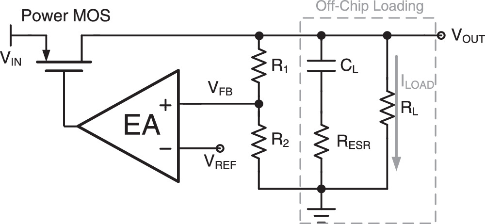
Figure 1 presents a conventional analog LDO, which consists of three main components, namely an error amplifier (EA), a power MOSFET, and a feedback network. The EA detects the difference between the reference voltage and the feedback voltage to control the current through the power MOSFET, thus adjusting the output voltage. This is achieved by dividing VOUT through resistors R1 and R2 after it is raised, ultimately stabilizing VOUT to the desired target voltage. The conventional analog LDOs typically offer higher linearity and noise immunity. However, to satisfy boundary conditions adequately, additional components such as resistors and capacitors are often introduced for compensation purposes.

Fig. 1. Conventional analog LDO.
Download figure:
Standard image High-resolution imageFigure 2 presents a simplified conventional digital control LDO, which consists of an error detection unit, an integral circuit, and a power MOSFET array. The comparator first determines the relationship between the reference voltage (VREF) and the output voltage (VOUT), and then, the digital control unit adjusts the power MOSFET array by controlling the number of PMOSFET transistors to be turned on or off. When conventional digital LDOs encounter significant load fluctuations, they often tend to generate voltage spikes, particularly when transitioning from light loads to heavy loads. This dropout phenomenon becomes more pronounced and has a highly adverse impact on the load circuit. Conventional digital LDOs typically respond to this by increasing the circuit clock frequency or boosting loop integration to achieve a faster transient response. However, this approach can lead to larger output ripples and higher power consumption. Moreover, wide variations in the load can still result in momentary voltage drops. As a result, we developed an innovative design approach tailored to wide load variation scenarios. Without altering the circuit clock frequency, we achieved a balance between power consumption and performance by adjusting loop gain. This approach aimed to overcome the trade-off between power and performance for such wide load variation circuits.
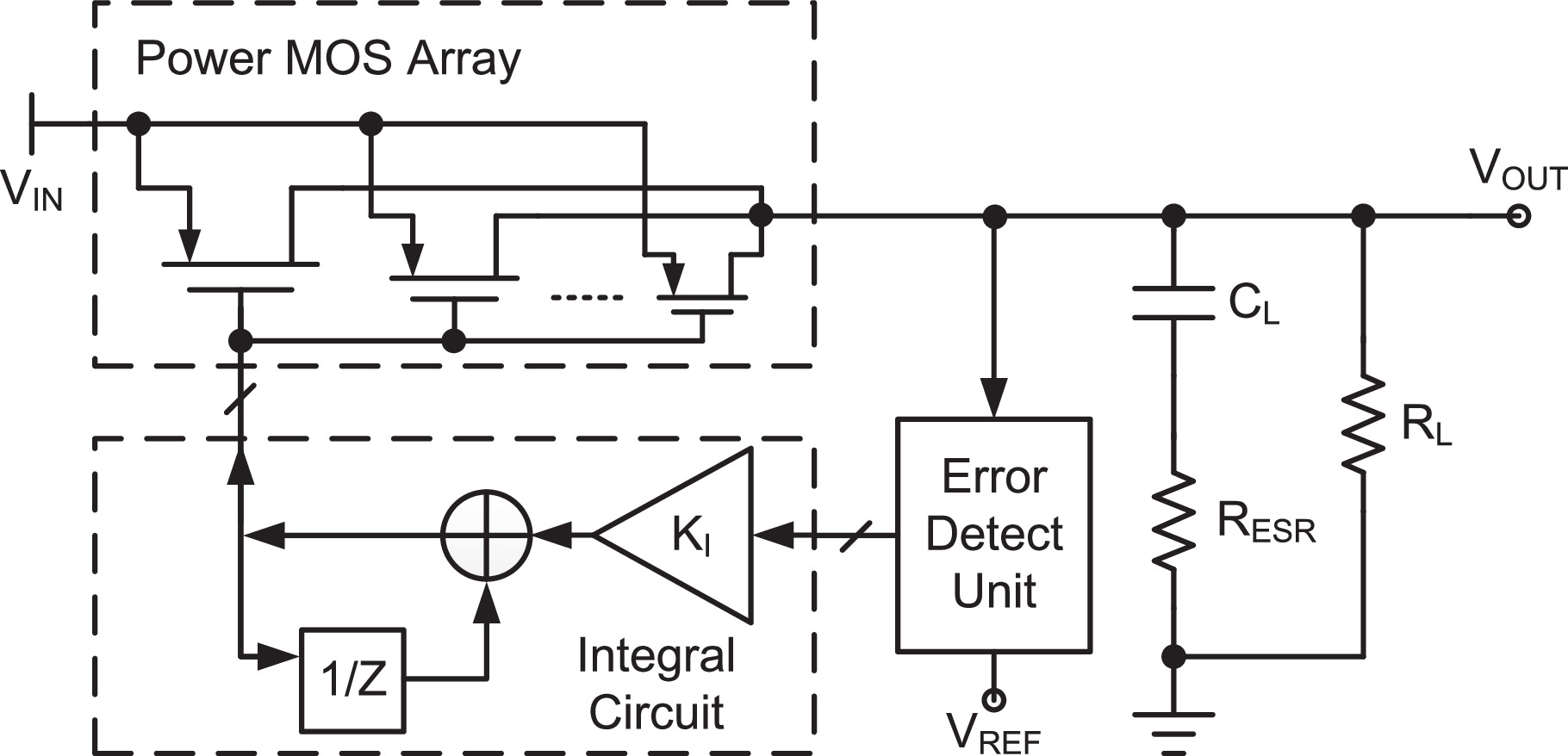
Fig. 2. Simplified conventional digital control LDO.
Download figure:
Standard image High-resolution imageThis article provides a detailed description of all of the circuits, serving as an extended version of our previous work. 15) Furthermore, it includes additional simulation and measurement results to showcase the performance of the proposed method. Various relevant papers related to our research have also been added to the list of references.
The structure of the rest of this article is as follows. In Sect. 2, we introduce the working principles of the proposed LDO. Section 3 describes the circuit implementation. Measurement results are presented in Sect. 4, and the conclusion is provided in Sect. 5.
2. Architecture and principle of the proposed LDO
As shown in Fig. 3, the proposed LDO was composed of a multi-phase error detection mechanism (MPED), a tri-stage damping selector (TSDS), a dynamic integration shift register (DISR), 16,17) and a power MOSFET array designed with both coarse and fine tuning. When the load changed, the MPED detected the real-time voltage variation at different phases of the input clock, 18,19) while the TSDS determined the unit integration amount on the basis of the real-time error size. Within a single period, the TSDS predicted the magnitude of load change on the basis of the variation at different phase points and determined the product of the loop gain. Finally, the DISR adjusted the on/off switching of the power MOSFET array according to the overall loop gain. 20) As the output voltage became stable, the TSDS gradually reduced the loop gain and adjusted the detection speed of the MPED to reduce the output ripple and lower the power consumption.

Fig. 3. Architectural diagram of proposed LDO.
Download figure:
Standard image High-resolution imageDesigning an LDO for wide load variations 21–26) is challenging because of the trade-off between input frequency and ripple. A high input frequency allows for a quick response to large load changes, but it also results in higher current consumption and lower current efficiency. Moreover, it can cause HF ripple in voltage regulation. In contrast, an LDO with lower input frequency and larger loop gain may not respond in time to wide load changes, resulting in severe voltage spikes. Additionally, there may be significant voltage ripples during steady-state operation. To address this issue, a MPED mechanism was utilized to achieve a real-time response similar to a high input frequency. A three-state damping selector and a dynamic integrator shift register were also used to adjust the loop gain and achieve a fast response, low ripple, 27–31) low current consumption, and high current efficiency.
3. Circuit description
3.1. TSDS
As depicted in Fig. 4, the three-state damping selector consisted of an overflow prevention unit, an mode (MOD) controller, and a dynamic integrator. The MOD signal controlled the integration size, while the MOD controller used the H/L CMP output of H/L_O as the fundamental basis for error size, taking into account the state of the circuit to determine the output of the MOD signal. This was mainly because of the characteristics of wide load changes, where the current changed significantly, and the information about voltage changes was limited for digital comparators. Therefore, we added the output of the multi-phase detection mechanism, MP_O [3:0], to consider the trend of changes over time in order to determine the timing of changes.

Fig. 4. Architecture of three-state damping selector.
Download figure:
Standard image High-resolution imageThe dynamic integrator further adjusted the integration product of the shift register. When the load changed significantly, the linear compensation speed of a single change was not sufficient to respond to changes in the output current in a timely manner. Therefore, when the MOD controller detected a significant trend change, the dynamic integrator increased the product quantity to accelerate compensation. When the compensation was sufficiently close to the reference voltage, the dynamic integrator reduced the product quantity to avoid significant system oscillations. When the MOD controller switched the unit integration, the dynamic integrator still provided a certain product quantity to accelerate the convergence of the steady state until it approached the reference voltage. Only then was the product quantity reduced to 1, switching to a unit linear compensation state, achieving a precise and minimal ripple voltage output.
Figure 5 presents a system flowchart of the MOD controller and dynamic integrator. When the change in the current voltage, ΔVE0, exceeded the preset comparison change, V0, the MOD output 1, using coarse adjustment, which meant a larger unit integration quantity. When the detection time points for the subsequent voltage trend (represented by ΔVE1) exceeded the comparison change, the system entered the dynamic integration mode and determined the product quantity on the basis of the total error sum obtained from different detection time points. It continued in the dynamic compensation mode until the accumulated error was less than a certain amount, and then, the system entered the unit integration mode. When the coarse adjustment integration stabilized, the system entered the fine adjustment integration. Similarly, on the basis of the voltage trend at different time points, the system determined whether to enter the adaptive compensation mode. The compensation mode continued until the voltage stabilized, and then, the system entered the steady-state regulating mode, completing the stability of the system and voltage. Finally, the overflow preventer detected the changes in the most significant bit and the least significant bit of the shift register, processed them, and sent the information to the MOD controller for adjustment and compensation.
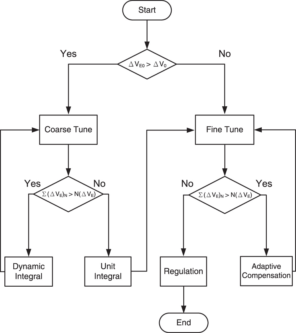
Fig. 5. Flowchart of MOD controller and dynamic integrator system.
Download figure:
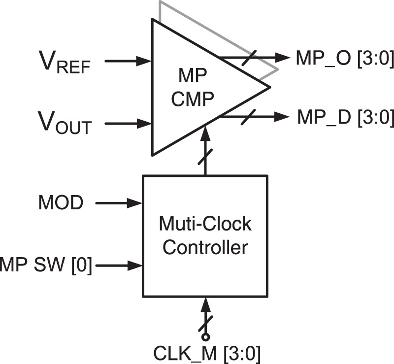
Standard image High-resolution image3.2. MPED
The multiphase error detection mechanism consisted primarily of a multi-phase comparator and a multi-error summary. Figure 6 depicts the architecture of a multi-phase comparator. The comparator consisted of four sets of comparators controlled by a multi-clock controller, which managed the four input phase clocks. The controller used the MOD and MP SW [0] signals to determine whether the comparators had to be activated and whether their results had to be sent to the multi-phase error summing block. In Fig. 7, a waveform diagram of a MPED mechanism is presented. Only when an MP_D [N] clock output triggered on the positive edge was the corresponding N-bit of MP_O output, indicating the direction of the error. A phase difference ΔΦ was observed between each pair of consecutive MP_D [N], allowing for four detections within a single input clock period. This enabled a lower clock rate to achieve a four-fold transient response, while the MOD = 0 and MP_SW [0] = 1 signals indicated a stable (regulated) output voltage, prompting the multi-phase mechanism to be turned off to reduce power consumption, enhance current efficiency, and minimize output ripple.

Fig. 6. Architecture of multi-phase comparator.
Download figure:
Standard image High-resolution image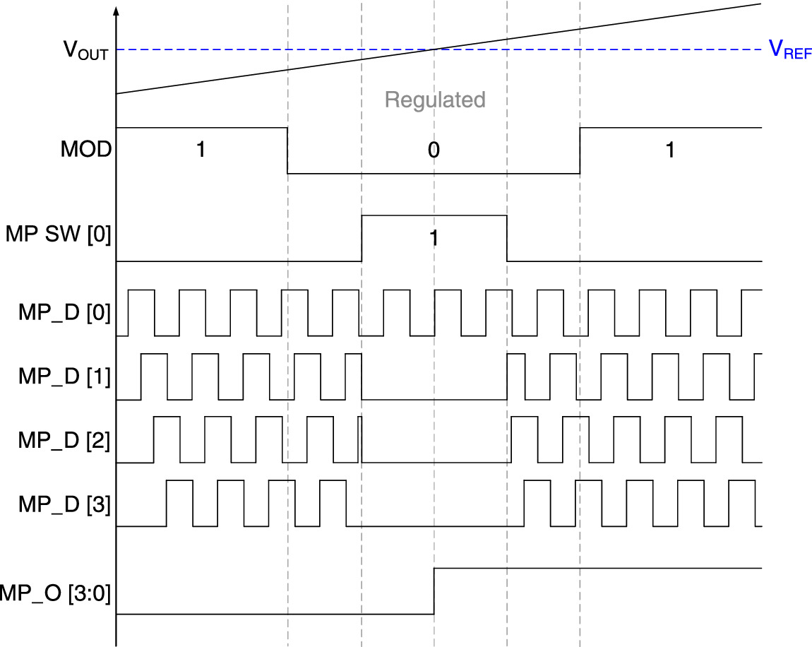
Fig. 7. Waveform diagram of a MPED mechanism.
Download figure:
Standard image High-resolution imageThe architecture diagram of the multi-error summing circuit is shown in Fig. 8. The individual phase outputs were controlled through MOD and MP SW [1:0]. When the multi-phase mechanism was enabled, the outputs of each phase were asynchronously transmitted to a shift register. However, when the multi-phase mechanism was disabled, the multi-error summing circuit was adjusted to synchronize the error output and perform error detection and correction once per cycle. Additionally, because of larger current variations under heavy loads, there were differences in the design thickness of the overall unit elements. The multi-error summing circuit also determined the size of the unit integration.

Fig. 8. Architecture of multi-error summing circuit.
Download figure:
Standard image High-resolution imageWhen MOD = 1 and the error voltage was higher, the detected MP_O [3:0] from Fig. 7 controlled the digital codes for U/D_C [3:0], determining the coarse integration, and was governed by MP SW [1:0] to control the output of MP_D [3:0] in order to achieve a rapid response with CLK_C [3:0] for swift restoration to the reference voltage level. When MOD = 0 and the error voltage was smaller, MP_O [3:0] was interpreted as a finer adjustment of the U/D_F [3:0] integration and was controlled by MP SW [1:0] with slower clock signals CLK_F [3:0] to reduce power consumption, ensure precise regulation, and minimize output ripple.
3.3. DISR
The architectural diagram for the DISR is shown in Fig. 9; it is divided into a coarse array and a fine array. Figure 10 illustrates the architecture of each group in the coarse array of DISR, with each group consisting of four units. The difference between the coarse and the fine arrays was primarily influenced by the DI signal, which affected the bit shift for each Q[n] with each CLK_C rising edge trigger. When CLK_C generated an upward edge trigger, the shift register operated. If U/D_C was logic 1, the shift register transmitted high-order bit values forward, and if it was logic 0, it would transmit values backward. The entire set of shift registers exhibited a continuous sequence of 0 and 1.
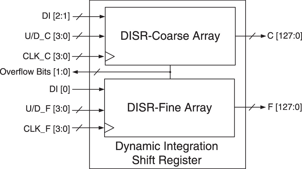
Fig. 9. Architecture of DISR.
Download figure:
Standard image High-resolution image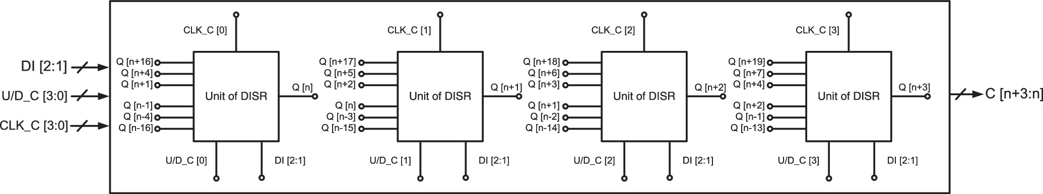
Fig. 10. Architecture of DISR coarse adjustment array.
Download figure:
Standard image High-resolution imageTraditionally, each rising edge trigger transmitted only one bit, meaning that only one Q value in the entire set of shift registers changed. While this method could generate highly linear and precise outputs, it clearly suffered from speed disadvantages. Therefore, the introduction of the DI signal to increase the shift amount was necessary. The DI signal in the coarse array was divided into two bits. When the low bit was 1, the shift amount increases by a factor of 4. When both bits were 1, the shift amount increased by a factor of 16. This design could significantly enhance the speed of the shift register, particularly for those with a large number of bits and the need to handle various loads.
3.4. Power MOSFET array
In the proposed digital LDO, as shown in Fig. 3, there were two different types of power transistor arrays, labeled as 40X and 1X, respectively. Both of these designs were regulated by the control mechanism from the preceding stage, which achieved linear variation control through shift registers. Therefore, we chose to use the same size design. The 40× power transistor array was controlled by the output signal C [127:0] from the previous stage's DISR, providing a larger current to enhance the overall transient response time. In contrast, the 1X power transistor array was controlled by the output signal F [127:0] from the preceding DISR, providing a smaller current to improve the accuracy of the output voltage and system stability. As both designs shared the same size and used binary doubling, one advantage of this uniform size design was that it helped to improve the linearity of the output current, thereby reducing the output voltage offset while mitigating the process variations. If the unit size of the power transistors was sufficiently fine, it could further suppress the amplitude of the output ripple.
4. Experimental results
4.1. Chip layout and measurement environment
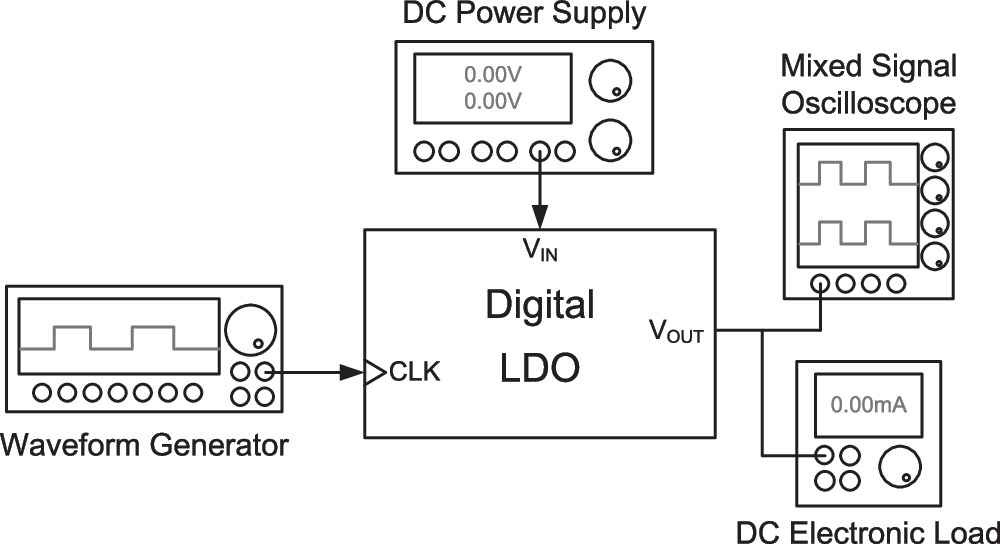
The proposed all-digital controlled LDO was implemented using the 0.18 μm standard CMOS process. The chip photograph and layout are shown in Fig. 11. The chip core area was 0.198 mm2. The large area covered on the chip photograph is the dummy layer required by the process; hence, the layout diagram is included for comparison. The measurement setup is illustrated in Fig. 12. An Agilent E3632A DC power supply was used to provide the required voltage and reference voltage for the circuit. The voltage sources for each sub-circuit in the digital LDO were separated during layout, including the voltage sources for the comparator, digital control circuit, and power transistor array. If the performance of individual sub-circuits was affected by a process variation, the circuit could be adjusted to operate normally by adjusting the various voltage sources or reference voltage. Prodigit 3302 F Dual DC Electronic Load served as the load current for the circuit, simulating the output load variations, and Keysight MSO5604A Mixed Signal Oscilloscope was used to capture the changes in the output voltage and measure the transient response of the circuit under load variations and the overall load regulation. The clock for the circuit was provided by the internal oscillator at 100 MHz. If the internal oscillator failed, Agilent 33522A Function/Arbitrary Waveform Generator switched to provide an external clock as a substitute to drive the LDO, and Keysight 34470A Digital Multimeter (7½ Digit) was used to measure the current consumption of the LDO circuit.

Fig. 11. Microphotograph and layout of proposed LDO.
Download figure:
Standard image High-resolution image
Fig. 12. Measurement and instrument setup.
Download figure:
Standard image High-resolution image4.2. Experimental results
The transient response simulation results for the load current of 0.5 mA and 200 mA were shown in Fig. 13, with three different scenarios, namely multiple-phase and dynamic integration mechanism, multiple-phase mechanism only, and no mechanism. It was observed that the multiple-phase mechanism could significantly reduce the voltage drop during the load transition, from a drop of the output voltage to 0 V to an improvement of only 0.26 V, a 74% improvement. The settling time could also be improved by approximately 30%. If the dynamic integration mechanism was added, the voltage drop could be further improved by 28.4%. When looking at the transition from heavy load to light load, the use of multiple-phase and dynamic integration mechanisms reduced voltage spikes by 60% and reduced the settling time by 81%. This clearly demonstrated that the multiple-phase and dynamic integration mechanisms could significantly improve the transient response across a wide range of load currents.
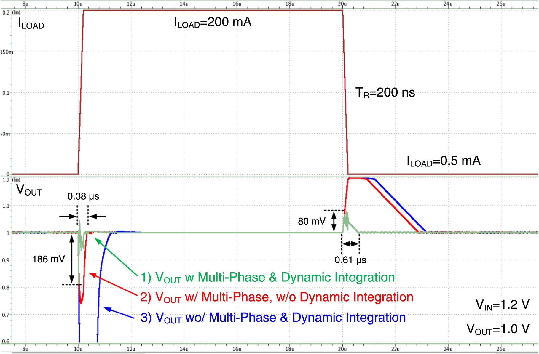
Fig. 13. Simulated load transient responses under different conditions.
Download figure:
Standard image High-resolution imageFigure 14 shows the measurement results for the light to heavy load transitions. It was observed that the output voltage remained stable around 1 V during load transitions from 0.5 to 100 mA, with a load regulation rate of 0.10 mV mA−1. The voltage transients during the transitions did not exceed 100 mV, and the response time was considerably short. However, the settling time was affected by the slew rate of the load, which was designed for 1 mA ns−1 in the simulation but limited to approximately 10 mA μ−1s−1 in the measurement because of the electronic load. This approximately 100 time difference resulted in some minor discrepancies in the voltage response during the load transition as compared to the simulation.
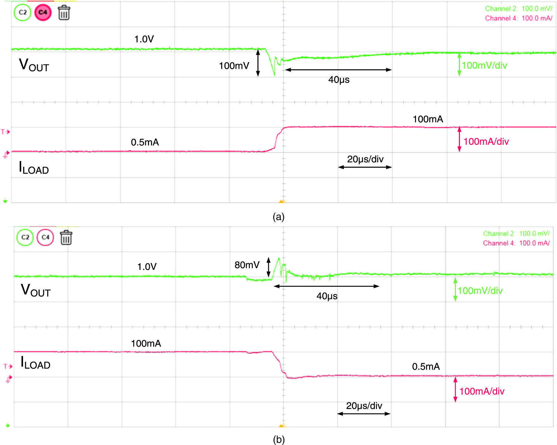
Fig. 14. Measured load transient responses: (a) response from light load (0.5 mA) to heavy load (100 mA) and (b) response from heavy load (100 mA) to light load (0.5 mA).
Download figure:
Standard image High-resolution imageFigure 15 illustrates the results of the line regulation measurement. The line regulation measurement was performed with the supply voltage varying from 1.2 to 1.4 V. According to the measurement results, the line regulation performance was 5.5 mV V−1 with a load current of 100 mA. In Fig. 15, there is some ripple observed in the ILoad. However, this is attributed to adjustments in the power MOSFET array corresponding to changes in VIN, leading to a corresponding variation in VOUT. This, in turn, influences the ILoad current and results in the observed ripple. Considering the variation in VIN, the presence of ripple in both VOUT and ILoad is regarded as a normal phenomenon. As VOUT stabilizes, the ILoad current eventually returns to a steady state. In the design of a LDO, utilizing a larger output load capacitance (CLOAD) does indeed contribute to reducing the output voltage ripple. However, it also leads to an increase in transient response time. In this LDO, a relatively larger CLOAD value is adopted to minimize the output voltage ripple. Simultaneously, to enhance transient response speed, a multi-phase and dynamic integration mechanism is proposed. As a result, the proposed LDO achieves an optimal balance between output ripple and transient response. The overall circuit specifications and comparison with relevant papers are shown in Table I. The figure of merit (FOM) values are listed in Table I. 18) ΔV represents the load regulation, CLOAD corresponds to the output load capacitance, IQ represents the quiescent current, and ΔILOAD represents the load current range. FOM is an indicator of the LDO's voltage regulation capability and power efficiency. For this FOM, a smaller value is more desirable, indicating that under appropriate load capacitor design, minimizing output voltage variation and static current is desirable. The proposed LDO design incorporates dynamic loop gain control technology achieve lower static current, improved load regulation, a broader range of load conditions, and higher peak current efficiency. Consequently, it exhibits favorable characteristics in terms of this FOM.

Fig. 15. Measured line transient responses: (a) when input voltage changed from 1.2 to 1.4 V and (b) when input voltage changed from 1.4 to 1.2 V.
Download figure:
Standard image High-resolution imageTable I. Performance comparison of contemporary digital LDOs.
| [14] | [18] | [19] | This Work | |
|---|---|---|---|---|
| Technology (nm) | 40 | 65 | 180 | 180 |
| Input voltage (V) | 0.6–1.2 | 0.6∼1.2 | 0.8–1.1 | 1.2–1.5 |
| Output voltage (V) | 0.55–1.15 | 0.4∼1.1 | 0.7–1.0 | 1 |
| Max. load current (mA) | 200 | 100 | 170 | 150 |
| Min. load current (mA) | N/A | 4 | 10 | 0.5 |
| Load regulation (mV/mA) | 0.7 | 0.64 | 0.11 | 0.10 |
| Quiescent current (μA) | 6–550 | 100~1070 | 500 | 110 |
| Peak current efficiency (%) | >99.7 | 99.5 | 99.71 | 99.93 |
| Settling time (μs)/Slew rate (mA/ns) | 104.2/1 | 1.24/0.1 | 0.08/2.4 | 40/0.01 |
| CLOAD (nF) | 0.15 | 1.5 | 0.04 | 1 |
| Core area (mm2) | 0.062 | 0.0374 | 0.3 | 0.198 |
| FOM 18) | 0.28875 | 0.086 | 0.362 | 0.073333 |

5. Conclusions
This paper proposed a fully digital low-dropout regulator for wide load range applications. To address the large current variations of wide loads, mechanisms were developed to achieve a fast response, low power consumption, and high current efficiency simultaneously. Multiple-phase error detection mechanisms enabled the circuit to achieve a transient response similar to a high input frequency at a lower input frequency. During wide load transitions, fast response and reduced voltage spikes were achieved while minimizing the dynamic power consumption. The dynamic integration design significantly improved the transient response during wide load changes while avoiding instability and a large ripple output caused by simply increasing the loop gain. However, because of instrumentation limitations, the stability time of the circuit during measurement was significantly longer. In the future, a high-speed load circuit will be designed to replace the electronic load to confirm whether the overall circuit mechanisms meet the original design specifications.
Acknowledgments
The authors would like to express their sincere gratitude to the National Science and Technology Council (NSTC) and the Taiwan Semiconductor Research Institute (TSRI), Taiwan, for their support in using EDA tools and fabricating the test chip.