

Abstract
A specially designed magnetron sputtering technique, the energy-filtering magnetron sputtering (EFMS) technique, was utilized to deposit aluminum nitride (AlN) thin films on Si (100) substrates. Improvements in the crystallization properties, surface morphology and optical properties of the films were studied. The results indicate that EFMS can be a useful technique for preparing high-quality thin films, which will be helpful in enabling potential applications of AlN thin film based microelectronic, optoelectronic and surface acoustic wave devices.
Export citation and abstract BibTeX RIS
AlN is a basic III–V semiconductor that has been used in various devices.1,2) With a wide direct band gap (Eg) and high thermal stability, AlN films can be used as sensing materials in ultraviolet detectors,3) and emission or transport layers in ultraviolet LEDs.4,5) They are also excellent substrates for AlGaN-based diodes since their lattice constants match well.6) In addition, AlN films with high preferred orientation are widely used in surface acoustic wave (SAW) devices due to their high SAW transmission rates and low acoustic loss.7,8) Considering the unique properties and broad application of AlN thin films, lots of effort has been spent on the investigation of their preparation and properties.
People have tried to synthesize AlN films with different preparation methods, such as CVD,9) pulsed laser deposition,10) molecular beam epitaxy,11,12) metal-organic CVD,13–15) and magnetron sputtering.16,17) Among them, magnetron sputtering technology is simple and could prepare thin films with high quality, uniformity, repeatability, and excellent adhesion to the substrate. This technology is also suitable for large-scale preparation and compatible with industrial production.2) However, the bombardments of high-energy particles during the magnetron sputtering process will cause various defects in the films.16,17) Therefore, the quality of thin films like AlN prepared by normal sputtering is yet to be optimized, especially for those deposited at lower temperatures in order to be applied in flexible electronic devices.18,19)
An improved DC magnetron sputtering (DCMS) technique for the preparation of AlN thin films is reported in this work, which is named the energy-filtering magnetron sputtering (EFMS) technique.20) AlN films prepared by EFMS show stronger preferred (002) orientation, higher uniformity, larger particles, and better, wider band gaps than those prepared by DCMS. This result indicates that EFMS can be a simple technique for depositing high-quality thin films.
An illustration of the EFMS technique is shown in Fig. 1. A metal mesh was placed between the anode and cathode as a filter electrode. The distance between the substrate and the filter was 25 mm and no shadows appeared on the film surface. The filter was connected to the substrate to make sure they were at the same potential. Electrons in the plasma were attracted by the filter electrode during the thin film deposition. The electrons would be absorbed directly by the filter electrode in moving to the anode, rather than hitting the thin films. Collisions of electrons with the thin films would be hindered and defects of the thin films would be reduced. Therefore, the surface uniformity, crystallinity and optoelectronic properties of the thin films would be improved.
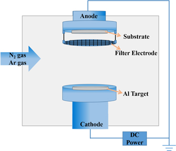
Fig. 1. (Color online) Illustration of EFMS.
Download figure:
Standard image High-resolution imageAlN films were deposited on Si (100) substrates by a JPG-560 vacuum multi-target magnetron coating equipment. The filter electrode was used with a mesh number of 8. A pure Al target was utilized as the Al source with a diameter of 50.8 mm and a purity of 99.999%. The sputtering gas was Ar (99.999%), and the reactive gas was N2 (99.999%). The sputtering parameters are shown in Table I. Before deposition, the Si substrates were first immersed in 5% HF solution for 1 min, and then cleaned with deionized water. After that, the substrates were ultrasonically cleaned by alcohol, acetone and deionized water in sequence for 15 min. Finally, the clean substrates were dried by nitrogen. In order to obtain uniform thin films, the substrate stage was rotated at a speed of 10 r min−1 by a motor during deposition. After deposition, the films were cooled to RT in the vacuum chamber.
Table I. Deposition parameters of AlN films.
| Sputtering power | 60 W |
| Base pressure | 2.5 × 10⁻⁴ Pa |
| Sputtering pressure | 0.6 Pa |
| Ar/N2 (sccm) | 25:25 |
| Deposition temperature (°C) | RT, 100, 200, 300, 400, 500 |
The crystallization properties of the thin films were characterized by an X-ray diffractometer (XRD, Smart Lab3KW), and the surface morphology by a field-emission scanning electron microscope (SEM, JSM-6700F) and an atomic force microscope (AFM, Solver NEXT) at RT. The optical properties of the films were characterized by an ultraviolet spectrophotometer (UH-4150). The resistance of the films was measured by a Hall-effect tester (ET-9000).
The optoelectronic properties of semiconductor materials are usually influenced by their crystallization properties. Besides, the textured surfaces of AlN thin films are beneficial for their application in LEDs and SAWs. To investigate the influence of substrate temperatures (Tdep) on the crystallization of the films, the XRD patterns of AlN films prepared using DCMS and EFMS at different Tdep, along with a reference pattern (03-065-3409), were obtained, as shown in Fig. 2. The diffraction peaks of the AlN thin films at 2θ = 33.53°, 36.28°, 38.26° and 50.23° can be assigned to the AlN (100), (002), (101), and (102) planes, respectively. The (002) peak was stronger than other peaks at all temperatures, indicating the preferential orientation of the deposited thin films. Similar (002)-oriented thin films deposited through DCMS were also reported by A. Pandey et al.21) The FWHMs of the AlN (002) peak obtained by JADE software as a function of Tdep are also listed in Fig. 2. The FWHMs of the (002)-oriented thin films deposited by the EFMS technique were smaller than those by DCMS, indicating larger grains and higher crystallization in the AlN thin films. Electrons in EFMS were diverted from the filtering electrode, reducing electron collisions in the thin film deposition. This helped to reduce defects inside or on the surface of the thin films, thus improving the crystallinity of the thin films. The high crystallinity of AlN thin films at optimized deposition conditions paves the way for their application in optoelectronic and SAW devices.
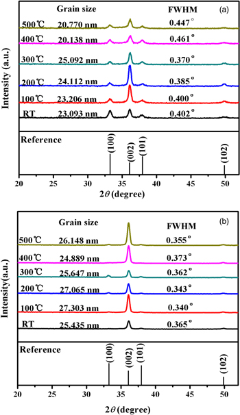
Fig. 2. (Color online) XRD pattern of the AlN films prepared by (a) DCMS and (b) EFMS at different Tdep.
Download figure:
Standard image High-resolution imageThe performance of optoelectronic and SAW devices can be influenced a lot by the thin film quality, including the surface morphology. A smooth surface is essential in forming a high-quality interface, which is critical to obtain functional layered devices. Thin films with pin holes cannot be utilized in layered structures due to possible short circuits. In order to investigate the surface information of the AlN thin films in this work, surface SEM images of the AlN films prepared by the DCMS and EFMS techniques at 400 °C were captured, as shown in Fig. 3. Nano-particles with uniform sizes and dense structures of the surfaces were shown under both conditions. However, the film prepared by EFMS was more uniform than that prepared by DCMS.
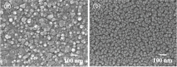
Fig. 3. SEM images of the AlN films prepared by the (a) DCMS and (b) EFMS techniques at 400 °C.
Download figure:
Standard image High-resolution imageThe quality of the thin films was also investigated by an AFM. The RMS surface roughness of 4 × 4 μm2 area AlN films prepared by DCMS and EFMS at different Tdep is shown in Fig. 4. The RMS roughness of the films prepared by the EFMS technique was generally less than that prepared by the DCMS technique. In particular, the minimum surface roughness was 0.9 nm at 400 °C, which is comparable with the 1.05 nm reported by T. Li et al.22) This can be attributed to the reduction of defects inside and on the surface of the thin films during the EFMS preparation process, improving the surface uniformity of the thin films. The initial increase of surface roughness can be attributed to the anisotropic growth of crystallites with increasing Tdep. With a further increase of Tdep until 500 °C, the adsorbed particles on the surface obtained enough kinetic energy by absorption of thermal energy from the substrate, thereby enhancing the surface migration and relaxation of the particles. This resulted in the latter decrease of surface roughness. The roughness analysis shows that a smooth and dense film can be prepared by optimizing the substrate temperatures.
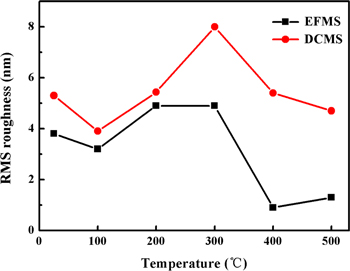
Fig. 4. (Color online) RMS roughness of AlN films prepared by DCMS and EFMS at different Tdep.
Download figure:
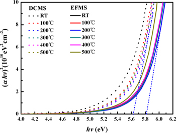
Standard image High-resolution imageThe band gap of an AlN film needs to be wide enough for short-wave LEDs and deep-ultraviolet photodetectors.4,23) In order to further illustrate the band gap change, the Eg values of the AlN films were also calculated. Near the absorption edge, the absorption coefficient α can be expressed as:24)

where d and T are the film thickness and transmittance, respectively. In direct band gap semiconductor materials, the relationship between the absorption coefficient and optical band gap can be expressed by the following Tauc relation:25)

where h is Planck's constant, v is the frequency of the incident light, and B is a constant. The relationship between (αhv)2 and hν was plotted, and then linear fitting was conducted to get the Eg value of the films, as shown in Fig. 5. The band gaps of the films prepared at different temperatures with the same technology did not change significantly. The Eg values of the AlN films prepared by EFMS were about 5.8 eV, higher than the 5.6 eV from the thin films prepared by DCMS. This may be attributed to the reduction of defects inside or on the surface of the thin films during the EFMS preparation process. The optical band gap in the vicinity of 5.7 eV slightly blue-shifted and then red-shifted with the increase of Tdep. In theory, the blue and red shifts of the optical band gap of semiconductors are attributed to an enhanced quantum size effect and Burstein–Moss effect and to the film stress, respectively. The blue shift of the optical band gap of an intrinsic semiconductor is usually explained by the quantum size effect. The decrease of crystallite size will result in a blue shift. To explain the blue shift result, the crystallite size data were added in Fig. 2. The change of crystallite size with the increase of Tdep cannot explain the blue shift result by the quantum size effect. To explain the red shift, the lattice strain [(c − c0)/c0, where c and c0 are the experimental and standard values of the c-axis lattice constant, respectively] data along the c-axis of the AlN films prepared by EFMS were added. The lattice strain values were −0.042%, 0.012%, 0.012%, −0.11%, 0.004%, and 0.072%, respectively, at Tdep of RT, 100, 200, 300, 400, and 500 °C. The lattice strain at Tdep of ≥200 °C is not consistent with the red shift result. Considering the minor change of the optical band gap with Tdep, we attribute the change of the optical band gap to errors in fitting and measurement.
Fig. 5. (Color online) Relationship between (αhv)2 and hν of the AlN films prepared by DCMS and EFMS at different Tdep.
Download figure:
Standard image High-resolution image
This study indicates that AlN films can be well deposited through the EFMS technique. AlN films with (002) preferred orientation were deposited on Si substrates. Combined XRD, AFM, and SEM studies and Eg calculations revealed that the quality of AlN films prepared by the EFMS technique is better than that of films prepared by the DCMS technique. These results demonstrate that preferred-orientation, smooth-surface AlN thin films can be prepared using the EFMS technique. This work could help the growth of better AlN films, facilitating their application in microelectronic, optoelectronic and SAW devices.
Acknowledgments
This work was supported by Science and Technology Projects of Henan Province (152102210038, 172102210106, 12b14007).