

Abstract
We report here a GaN-based resonant cavity light-emitting diode (RCLED) with top and bottom dielectric TiO2/SiO2 distributed Bragg reflector (DBR) mirrors on a silicon substrate. High data transmission in free space at 200 Mbps with an opening in the eye diagram was achieved. The results show that the combination of GaN-based LED on silicon and double sided dielectric DBR mirror deposition enables a manufacturable process which provides a unique opportunity for commercialization of RCLED in future solid-state lighting and visible light communication applications.
Export citation and abstract BibTeX RIS
Compared to conventional light-emitting diodes, resonant cavity light-emitting diodes (RCLEDs) have several advantages, including high spectral purity, superior emission directionality, stable peak wavelength, improved out-coupling efficiency and high light extraction efficiency.1–3) Due to these inherent features, RCLEDs have been adopted in various optoelectronic applications, especially in those applications where the emitted light has to be coupled into the optical systems with given numerical apertures, such as plastic optical fiber-based networks, line-of-sight visible light communications (VLCs), optical scanners, speckle free illumination, printers and display applications.4–7) Numerous studies on RCLED have been reported. Reference 8 presented efficient InGaN-based RCLEDs in which a two-pair Ta2O5/SiO2 distributed Bragg reflector (DBR) and a metallic Ag layer were used to form a structure containing an optical cavity. Reference 9 demonstrated a GaN-based RCLED featuring a Si-diffusion-defined confinement structure which is an effective means to reduce aperture size. Reference 10 reported green InGaN-based RCLEDs which were transferred from sapphire substrate to Si substrate using laser lift-off and wafer bonding techniques. Reference 11 showed the realization of CW near-milliwatt-power emission at 390 nm from RCLED on GaN templates in which a bottom AlGaN/GaN DBR and a top dielectric SiO2/ZrO2 mirror were employed to form the vertical cavity. However, the reported RCLEDs are usually implemented on the GaN-on-sapphire or GaN-on-GaN platform. Compared with the two substrates, silicon substrate has unique advantages. High-quality GaN has been epitaxially grown on silicon substrate by managing the huge mismatch in the coefficient of thermal expansion and the large mismatch in lattice constant between GaN and silicon.12–15) III–nitride-on-silicon wafers has a great potential in reducing the production cost and making mass-production available.16–18) Various silicon-based light sources have attracted worldwide research interests and played an important role in the energy-efficient solid state lighting market.19-22)
In this study, we propose to fabricate and characterize a blue RCLED on the GaN-on-silicon platform using the combination of silicon substrate removal, back epitaxial wafer thinning and dielectric DBRs deposition techniques. The device structure consists of a suspended membrane InGaN/GaN multiple-quantum-well light-emitting diode (MQW-LED) sandwiched by two dielectric TiO2/SiO2 DBR mirrors which is able to form a vertical Fabry–Pérot cavity. The top DBR mirror was fabricated before the metal electrode deposition and the bottom DBR mirror was completed after silicon substrate removal and back wafer thinning of the epitaxial film. With the removal of the silicon substrate, the absorption of downward-emitting light by silicon are eliminated.23,24) And back epitaxial wafer thinning is beneficial for the increase of carrier concentration and the decrease of spreading resistance leading to performance improvement of the suspended membrane MQW-LED.25,26) In addition, back epitaxial wafer thinning also completely removes the defect-rich buffer layer which can reduce the optical cavity loss. Highly reflective DBR mirrors are key components for high-performance RCLEDs, especially for GaN-baaed RCLEDs.10) Lots of efforts have been made in the growth of semiconductor DBR pairs, including InAlN/GaN and AlGaN/GaN Bragg reflectors,27–29) and various optoelectronic devices have been fabricated with such semiconductor DBR mirrors. However, in comparison with semiconductor DBR mirrors, dielectric DBR mirrors are capable of providing a wider optical stopband, higher reflectivity and can be easily integrated with nitride light emitters to form efficient optical resonators. We present here detailed analysis on the electrical and optical characteristics of the fabricated RCLED.
The fabricated RCLED consisting two dielectric TiO2/SiO2 DBR mirrors was implemented on a commercial LED wafer. The GaN heterostructure structures were grown on the silicon substrate, as shown in Fig. 1. The active region includes nine 3 nm InGaN quantum wells with 10 nm GaN barriers, surrounded by an upper 220 nm p-type GaN layer and a lower 3200 nm n-GaN layer. Al-composition grade AlGaN/AlN buffer layers have been utilized to build up a compressive strain for compensating the tensile stress in the process of growth and filter out the threading dislocations to obtain crack-free high-quality n-type GaN layer on silicon substrate.12) Chemical mechanical polishing was used to thin the LED wafer to 200 μm for further silicon substrate removal.
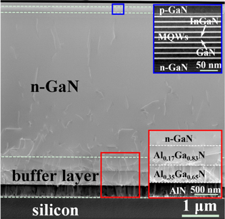
Fig. 1. (Color online) Cross-sectional high-angle annular dark-field (HAADF) scanning TEM image of GaN-on-Si LED epitaxial film.
Download figure:
Standard image High-resolution imageThe schematic fabrication process of the proposed RCLED is illustrated in Fig. 2. The process begins with the p-type mesa etching down to n-type GaN layer by using inductively coupled plasma reactive ion etching with Cl2 and BCl3 hybrid gases. Then an 8.5-pair dielectric stack with alternating λ/4 thick TiO2/SiO2 layers was deposited on the mesa region using a combination of electron beam evaporation and lift-off processes. The DBR located in the luminescent region of the p-type mesa acts as the top mirror providing a reflectivity of 99.4% and the DBR in other region are used as an isolation layer between p-type GaN and p-electrode in order to increase the device's current density. Both p- and n-electrodes were then formed with the 50/100/500 nm Ti/Pt/Au metallization stacks by a combination of metal evaporation, lift-off processes and rapid thermal annealing under N2 gas for 5 min. After that, the silicon substrate and the defect-rich buffer layer were selected etched away by deep reactive ion etching technique. Finally, another 7.5-pair dielectric TiO2/SiO2 DBR with a reflectivity of 92.7% was deposited on the suspended membrane from the backside to serve as the bottom mirror.
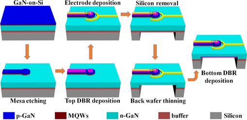
Fig. 2. (Color online) RCLED fabrication process flow.
Download figure:
Standard image High-resolution imageShown in Figs. 3(a)–3(c) are the top view scanning electron microscope (SEM) images for the fabricated RCLED. The diameters for the top p-metal electrode, top dielectric TiO2/SiO2 DBR, and p-mesa are 5 μm, 15 μm, and 25 μm, respectively. The gap between the bottom n-ring-electrode and the edge of the circular p-type mesa is 10 μm. The DBR located in the bonding region of the p-type mesa acts as the isolation layer between the p-electrode and the p-type GaN. With the introduction of DBR isolation layer, the physical dimension of the RCLED decreases and the junction capacitance reduces, leading to the reduction of RC (resistive–capacitive) time constant and the faster modulation rate.30) Figure 3(d) shows the morphology of the backside of RCLED before bottom mirror deposition. A rectangular micro pit with height of 198.5 μm was formed using the combination of the silicon substrate removal and back epitaxial wafer thinning. The device located on the topside of the suspended GaN membrane can be clearly observed from the backside because GaN membrane is transparent. And the GaN membrane is strong enough and can be taken as bottom mirror's carrier due to its stable thermal, chemical and mechanical characteristics.31,32)
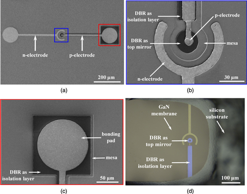
Fig. 3. (Color online) (a) SEM image of the RCLED. (b) High magnification SEM image of the resonant cavity from the topside. (c) High magnification SEM image of the bonding area. (d) Optical micrograph of the RCLED viewed from the backside.
Download figure:
Standard image High-resolution imageFigures 4(a) and 4(b) show the measured reflectivity spectra of the 8.5-pair dielectric TiO2/SiO2 DBR (top mirror) and the 7.5-pair dielectric TiO2/SiO2 DBR (bottom mirror), respectively. A peak reflectivity of 99.4% and a large stop-band of 82 nm were obtained in the measured reflectivity spectra of the top mirror. The reflectivity of the bottom mirror (92.7%) is lower than that of the top mirror (99.4%) at 450 nm which favors the bottom-emission type RCLED application. The cross-sectional SEM images of the top mirror and bottom mirror are demonstrated in Figs. 4(a) and 4(b), respectively, indicating the alternating deposition and good periodic arrangement of the TiO2 and SiO2 layers. TiO2 layers and SiO2 layers can be clearly distinguished due to the sharp interfaces between them. The two DBR mirrors were deposited under the same conditions. The relatively larger surface roughness due to the back epitaxial wafer thinning also reduces the reflectivity of the bottom mirror to certain extent.
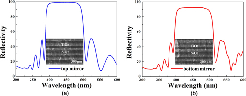
Fig. 4. (Color online) Experimental reflectivity spectra of the dielectric reflective DBRs: (a) top mirror; (b) bottom mirror.
Download figure:
Standard image High-resolution imageShown in Fig. 5 are the measured light–current–voltage (L–I–V) plots. The RCLED exhibited a turn-on voltage of approximately 2.8 V. Above the turn-on voltage, the current density increased rapidly with increasing forward bias voltage and the current density increased to 462.19 A cm−2 under the applied voltage of 8.0 V, which indicates favorable processing quality and excellent electrical performance. The light output of the RCLED demonstrates linear relation with the injection current density indicating an excellent electrical-to-optical (E/O) conversion efficiency.

Fig. 5. (Color online) Measured RCLED L–I–V characteristics.
Download figure:
Standard image High-resolution imageThe optical characteristics of the non-resonant LED and RCLED were investigated using electroluminescence (EL) measurements, as demonstrated in Fig. 6(a). The non-resonant LED and RCLED have the same structure but there are no top and bottom DBR mirrors on it. The emitted light was examined from the backside-surface-normal direction of both devices at room temperature. Compared with non-resonant LED, linewidth narrowing of the emission spectrum for RCLED was observed. The full wave at half maximum (FWHM) of the RCLED's EL spectrum is 15 nm, while the FWHM of the non-resonant LED's EL spectrum is 27 nm. Moreover, the EL intensity of the RCLED is 1.6 times magnitude than that of the non-resonant LED under injection current of 100 μA, as shown in the inset of Fig. 6(a). The increasement of the EL intensity is mainly attributed to the higher emission directionality from the resonant effect of the vertical Fabry–Pérot cavity. Figure 6(b) shows the EL spectra of the RCLED under injection current levels of 50–200 μA at room temperature. The emission normal to the wafer surface was captured from the backside and the EL peak wavelength located at 449.5 nm was measured. With increasing the injection current, the EL peak remained stable indicating a good stability of peak wavelength at various injection currents. The emitted light intensity at EL peak wavelength and the injection current also shows an approximate linear relation, as demonstrated in the inset of Fig. 6(b). The ratio of the EL peak intensity between 100 and 50 μA is 1.82. And when the injection current increases to 150 and 200 μA, the ratio increases to 2.69 and 3.56 accordingly, which indicates that the emitted light intensity can be effectively modulated by changing the injection current. The characteristics of the fabricated RCLED show the capability for a diverse range of light communication applications ranging from optical interconnect within photonic integrated circuits through indoor wireless communication to outdoor inter-building signal transmission.
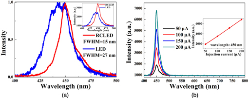
Fig. 6. (Color online) (a) EL spectra of RCLED and non-resonant LED, with the inset shown the different EL intensities under injection current of 100 μA. (b) EL spectra of the RCLED under various injection currents, with the inset shown the peak intensities at different injection current levels.
Download figure:
Standard image High-resolution imageFree space VLC experiment was conducted to characterize the high-speed data transmission of the fabricated RCLED. The setup of free space VLC is schematically show in Fig. 7(a). An Agilent 33522A arbitrary waveform generator is used to generate pseudo-random binary sequence (PRBS) data stream. The PRBS signals are amplified and biased with a bias-tee circuit before they are applied to the fabricated RCLED which acts as a signal transmitter. The transmitter converts the electrical signals into light pulses, the light pulses are transmitted via free space and sequentially converted back into electrical signals by a Hamamatsu C12702-11 photodiode module which integrates a current-to-voltage converter, a temperature-compensation bias circuit and an avalanche photodiode. Finally, the amplified electrical signals are analyzed by an Agilent DSO9254A digital storage oscilloscope. Figure 7(b) demonstrates the eye diagram measured at 200 Mbps. A clear opening is observed in the eye diagram, indicating a great permissible error for noise and jitter of the free space VLC system.

Fig. 7. (Color online) (a) Schematic diagram of the experimental setup for free space VLC; and (b) measured eye diagram at 200 Mbps.
Download figure:
Standard image High-resolution image
We fabricated and demonstrated a blue RCLED incorporating top and bottom dielectric DBR mirrors on the GaN-on-silicon platform. The electrical, optical and communication characteristics of the RCLED were measured. The fabricated RCLED exhibits excellent electrical performance and obvious linewidth narrowing of the emission spectrum. The resonant peak wavelength remained stable under various injection currents. The free space VLC with PRBS transmission rates up to 200 Mbps was experimentally demonstrated. The combination of GaN-based LED on silicon substrate and double sided dielectric DBR mirror deposition enables a manufacturable process, providing a unique opportunity for commercialization of vertical cavity surface emitters in future solid-state lighting and VLC applications.
Acknowledgments
Special Project for Inter-government Collaboration of State Key Research and Development Program (2016YFE0118400); Natural Science Foundation of Jiangsu Province (BE2016186); National Natural Science Foundation of China (61322112, 61531166004); Research Project (CKJA201705); the "111" project.