

Abstract
Benefiting from its unique electrical and optical properties, graphene as a saturable absorber (SA) has been widely explored. However, it is still challenging to develop SAs with large modulation depths due to the weak absorption of the monolayer graphene. Here a graphene-on-slot waveguide configuration was demonstrated to overcome this limitation. From the experimental study, with only 20 μm long graphene, the graphene-on-silicon slot waveguide exhibited lower saturation energy of 313 pJ and seven times larger modulation depth, compared with a graphene-on-silicon nitride rib waveguide. Our study paves the way for the development of ultra-compact graphene-on-waveguide SAs for ultrafast lasers and nonlinear optics.
Export citation and abstract BibTeX RIS
Graphene has many unique electronic and optical properties, such as ultrahigh electron mobility, zero bandgap and tunable absorption, which is promising for various photonic and optoelectronic applications.1–3) Especially, benefiting from the linear dispersion relation of electrons in a narrow range around the Fermi level, optical interband transitions in graphene are wavelength independent in a broad spectral region from visible light to mid-infrared wavelengths4,5) and can be easily saturated with high power excitations. Therefore, saturable absorbers (SAs) based on graphene provide ideal solutions for ultrafast lasers, owing to their wideband tunability. These SAs are mostly constructed by integrating chemical vapor deposition (CVD) graphene or graphene-polymer composite on an optical fiber pigtail end6) or a mirror,7) which are fragile to the optical power induced thermal damage and eliminating the graphene absorption, due to the atomic interaction length in normal incidence conditions. Although other evanescent-field interaction schemes of SAs with graphene integrated on D-shaped fibers8,9) or microfibers10) can enlarge the overlap between graphene and the optical mode as well as circumvent the thermal damage, those configurations may suffer from perturbations induced by environmental variations and have limited optical interaction enhancement. Therefore, it is highly required to develop robust graphene SAs with strong light-graphene interactions and large modulation depths.
On the other hand, by integrating graphene with photonic integrated waveguides, the evanescent-field coupling can elongate the optical interaction length and therefore enhance the optical absorption towards 100%,11,12) compared with 2.3% absorption in the normal incidence case. Therefore, combing with graphene, the hybrid photonic integrated circuit is a promising integrated platform for various optoelectronic applications.13–18) Linear and nonlinear optical absorptions of graphene-on-rib/strip waveguides have been experimentally characterized in previous studies.19,20) Besides, to further enhance the optical interaction between graphene and propagating light in the waveguide, novel waveguide structures, such as graphene horizontally sandwiched in dielectric waveguides,21) have been theoretically proposed. The optical mode is confined in the subwavelength low index slot region in the middle where graphene is integrated, which is explained by the discontinuity of the electric field at the high-refractive-index (RI)-contrast interface. Therefore, the optical interaction in the graphene-on-slot waveguide is enhanced. However, as far as we know, it is still challenging to realize such configurations in experiment due to fabrication difficulties.
In this work, we proposed to use the silicon (Si) vertical slot waveguide,18,22,23) as shown in Fig. 1(a), to achieve an SA with a large modulation depth as well as ultra-compact footprint. Figure 1(b) is the schematic of electrical field distributions of different graphene-on-Si waveguide configurations. The TE mode slot waveguide is able to confine and guide the higher intensity of light in the slot region, so the graphene can have a much stronger interaction with the propagating light after integrated with the slot waveguide configuration, leading to reinforced graphene-on-waveguide optical absorption and a significant reduction in footprint. Besides, compared with our previous study,24) saturable absorption behaviors of different graphene-on-waveguide configurations were experimentally measured and comprehensively compared by using a pulsed laser at 1550 nm wavelengths. The graphene-on-Si slot waveguide was demonstrated with a lower saturation energy and larger modulation depth, compared with the graphene-on-silicon nitride (SiN) rib waveguide.

Fig. 1. (Color online) Schematics of graphene-on-waveguide devices. (a) Schematic of the graphene-on-silicon slot waveguide. (b) Schematic of electrical field distributions of TE/TM silicon slot waveguides and strip waveguides with graphene integrated on top.
Download figure:
Standard image High-resolution imageThe TE mode slot waveguide was designed on a commercial silicon-on-insulator wafer with 250 nm silicon and 3 μm buried oxide (BOX), consisting of two strip waveguides with 250 nm width separated by a 70 nm slot. The relative permittivity of graphene was calculated at 0 eV Fermi level for 1550 nm wavelength by using Kubo formula.25) By employing the calculated relative permittivity in a finite element method simulator (COMOSOL Multiphysics), complex RIs of different graphene-on-waveguide modes were calculated. The optical absorption coefficient of the TE mode graphene-on-Si slot waveguide was calculated to be 0.94 dB μm−1, which was larger than those of the TM mode graphene-on-Si slot waveguide (0.59 dB μm−1) and TE/TM mode graphene-on-Si rib waveguides (0.34 dB μm−1 and 0.64 dB μm−1, respectively). Besides, the effective RI of the TE mode graphene-on-Si slot waveguide was calculated to be 1.6449, which was also less than those of the TM mode graphene-on-Si slot waveguide (1.6917) and the TE/TM mode graphene-on-Si rib waveguides (2.6018 and 1.9109, respectively). So the less mode confinement may also contribute to the larger optical absorption of the TE mode graphene-on-Si slot waveguide. For comparison, we designed a graphene-on-rib waveguide on a customer-designed SiN wafer with 720 nm low-pressure CVD grown SiN and 4 μm BOX. The width and etching depth of the SiN waveguide were 1.2 μm and 400 nm, respectively. Optical absorption coefficients of TE/TM mode graphene-on-SiN rib waveguides were calculated to be 0.02 dB μm−1 and 0.03 dB μm−1, respectively.
Graphene-on-waveguide devices were fabricated by using standard nanofabrication methods. Si waveguides and SiN waveguides were fabricated by using electron beam lithography (EBL) and deep reactive-ion etching. Subwavelength grating couplers26) and one dimensional (1D) uniform focusing grating couplers were applied for Si waveguides and SiN waveguides, respectively, to couple the TE mode light into and out of waveguides, as shown in scanning electron microscope images of Figs. 2(a) and 2(c), respectively. A Y junction was used in the Si slot waveguide as the mode converter between the strip waveguide and the slot waveguide. Then CVD graphene was integrated on waveguide devices by using a wet transferring method which was described as follows. The commercial graphene on copper foil covered by polymethyl methacrylate (PMMA) was first immersed in the ammonium persulfate solution to remove the copper beneath. Next, the graphene covered by PMMA was rinsed by the deionized water. After drying in the air, the photonic chip was baked at 150 °C for 15 min to melt the PMMA resist, allowing better contact between graphene and waveguides. Later the photonic chip was baked at 80 °C for 30 min on a hot plate so that the steam could improve the adhesion of graphene. Finally, the photonic chip was immersed in acetone for 15 min to remove the covered PMMA. The length of the graphene-on-SiN waveguide was 500 μm, as shown in Fig. 2(d). On the other hand, the length of graphene integrated on the Si slot waveguide was tailored to 10 μm, 20 μm, 30 μm, 40 μm, 50 μm, and 60 μm, respectively, by using EBL and O2 plasma etching. As shown in Figs. 2(a) and 2(b), the area with and without graphene was identified from the contrast of images. The graphene integrated on the Si slot waveguide was measured by using Raman spectroscopy. As shown in Fig. 3, the ratio of G peak (1588 cm−1) to 2D peak (2690 cm−1) was smaller than 0.5, indicating the monolayer graphene structure.27)
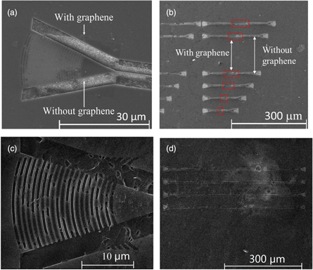
Fig. 2. (Color online) SEM images of graphene-on-waveguide devices. (a) SEM image of the fabricated Si subwavelength grating coupler. (b) SEM image of the Si slot waveguides with different lengths of graphene integrated on top. The area with and without graphene can be clearly identified through the contrast of the image. (c) SEM image of the 1D uniform focusing SiN grating coupler with graphene integrated on the surface. (d) SEM image of graphene-on-SiN waveguides.
Download figure:
Standard image High-resolution image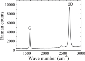
Fig. 3. Raman spectroscopy characterization of the graphene integrated on the slot waveguide.
Download figure:
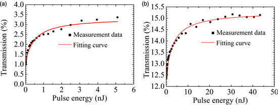
Standard image High-resolution imageThe transmission of the graphene-on-slot waveguide with graphene length of 20 μm was measured by using a home-built gain-switched pulsed laser, with 50 ps pulse width and 1 MHz repetition rate centered at 1555.65 nm. The laser was amplified and the output was subsequently filtered by an optical bandpass filter. A 5% tap was used to monitor the input power. The other 95% was coupled into the graphene-on-Si slot waveguide from a fiber polarization controller. The TE mode subwavelength grating had a coupling efficiency of 25%. The transmission at different pulse energies, excluding coupling losses of the input and output grating couplers, was shown in Fig. 4(a). The measured transmission at a low pulse energy of 4.98 pJ was 0.99%, indicating a measured optical absorption coefficient of ∼1 dB μm−1, which was consistent with the theoretical calculation. When the pulse energy increased to 198 pJ, the transmission was 1.90%, indicating that the increased concentration of excited electrons results in band filling and begins to block some absorption. Besides, the transmission of the graphene-on-slot waveguide with a length of 30 μm was measured but the transmission continuously increases with increasing the pulse energy up to 15 nJ. Further increasing the pulse energy results in the device damage due to the large photothermal heat generation, coming from the strong graphene-light interaction in the graphene-on-silicon slot waveguides. Consequently, the length of the integrated graphene should be optimized with respect to optical powers in order to achieve effectively saturable absorption. The graphene-on-SiN waveguide optical transmission was also measured, as shown in Fig. 4(b). The measured transmission at a low pulse energy of 20 pJ was 12.3%, indicating an optical absorption coefficient of ∼0.02 dB μm−1, which also agreed with the theoretical calculation. The transmission gradually saturated when the pulse energy was larger than 16.9 nJ.
Fig. 4. (Color online) Transmissions of graphene-on-waveguides at different input power levels. (a) Transmission of the graphene-on-Si slot waveguide at different input optical pulse energies. (b) Transmission of the graphene-on-SiN waveguide at different input optical pulse energies.
Download figure:
Standard image High-resolution image
And then, saturable absorptions of graphene-on-waveguide devices were analyzed by using the two-stage model which is widely used for two-dimensional quantum wells. The graphene-on-waveguide absorption was calculated from T = e−αL, where α (μm−1) and L (μm) were the attenuation coefficient and the length of graphene integrated on the waveguide, respectively. The attenuation coefficient is defined by28)

where αS and αNS are the saturable and non-saturable absorption components, and ES is the saturation pulse energy. For the graphene-on-Si slot waveguide, αS, αNS, and ES were fitted to be 0.053 μm−1, 0.17 μm−1, and 313 pJ, respectively. While for the graphene-on-SiN waveguide, αS, αNS, and ES were fitted to be 0.000 42 μm−1, 0.0038 μm−1, and 2.832 nJ, respectively. The modulation depth is defined as

The modulation depths were calculated to be 1.89 for the graphene-on-silicon slot waveguide and 0.24 for the graphene-on-SiN waveguide. Therefore, compared with the graphene-on-SiN waveguide, the graphene-on-Si slot waveguide had a much lower saturation energy and ∼7 times larger modulation depth, which can be explained by the significant enhancement of the optical interaction of the graphene-on-slot waveguide configuration as well as the reduced length of graphene integrated on the surface of the waveguide.
In summary, the graphene-on-Si slot waveguide was demonstrated to enhance the in-plane optical interaction in graphene-on-waveguide configurations. The saturable absorption behaviors of the graphene-on-Si slot waveguide and graphene-on-SiN rib waveguide were experimentally studied. Owing to the enhanced optical interaction as well as the small area of graphene, the saturable absorption of the graphene-on-Si slot waveguide configuration was observed with low saturation energy of 313 pJ and seven-time improvement in modulation depth, compared with the graphene-on-SiN waveguide. Therefore, the graphene-on-Si slot waveguide is a good candidate for SAs with large modulation depths in ultrafast lasers and promising for nonlinear optical processing applications.
Acknowledgments
This work is supported by National Science Foundation of China (No. 61805164, No. 61775149, and No. 61505239), Natural Science Foundation of SZU (No. 85302-000170), Shenzhen Research Foundation for Talented scholars (No. 000309), Shenzhen Science and Technology Project (No. JCYJ20160226192754225, No. JCYJ20160307145209361, and No. JCYJ20160307111047701), Guangdong Natural Science Foundation (No. 2016A030313059), and Science and Technology plan project of Guangdong (No. 2017A010101018).