

Abstract
GaN PolarMOS is a vertical power transistor incorporating the unique polarization-induced bulk doping scheme in III-nitrides for the body p-n junction. We report the realization of this device, wherein the vertical channel, source contact, and body contact regions are successfully formed using three steps of selective-area epitaxial regrowth, all by molecular beam epitaxy (MBE). The fabricated PolarMOS has an excellent on-current of >500 mA mm−1 and a specific on-resistance of 0.66 mΩ · cm2. The reverse breakdown mechanisms of the PolarMOS are investigated. First, a pronounced source-drain vertical leakage is identified and attributed to the passivation of the buried p-type body, which is subsequently resolved by the sidewall activation method. With the body leakage eliminated, the breakdown voltage is found to be limited by a highly conductive path along the regrowth sidewall interface using the conductive scanning probe technique, despite the absence of apparent structural defects.
Export citation and abstract BibTeX RIS

Content from this work may be used under the terms of the Creative Commons Attribution 4.0 license. Any further distribution of this work must maintain attribution to the author(s) and the title of the work, journal citation and DOI.
1. Introduction
There has been growing interest in GaN-based power electronic devices in recent years, driven by excellent material properties leading to a unipolar figure of merit exceeding that of Si and SiC, as well as unique doping schemes employing the inherent polarization physics. Indeed, the promising unipolar limit has been confirmed by the vertical p-n junction diodes fabricated on single-crystal substrates with avalanche breakdown.1–8) The absence of ionized-impurity scattering, together with a strong carrier confinement in the polarization-doped heterojunction 2-dimensional channel in the c-plane of III–V nitrides, allows for a high room-temperature electron mobility insensitive to dislocation scattering,9) even when grown on foreign substrates. For example, low cost and high performance can be simultaneously obtained in lateral GaN high-electron-mobility transistors (HEMTs) grown on Si substrates, which have already been commercialized for power applications.10)
In comparison with the lateral HEMTs, vertical power transistors can offer important advantages such as higher current density, better reliability, and avalanche capability if an electrically connected p-type body is used. Various types of GaN vertical transistors have been demonstrated, including current aperture vertical electron transistors,11–14) trench-MOSFETs,15–19) vertical diffused MOS (VDMOS)-like transistors,20,21) vertical fin power FETs,22–24) as well as trench-MOSFETs with a thin regrown channel.25–30) Despite the promising progress, the figures of merit of the currently reported devices have not yet reached the GaN limit. One of the major reasons is the difficulty in realizing high-quality lateral p-n junctions due to the immature selective-area doping technology. Lateral p-n junctions offer important functionalities in vertical power devices. Among those functionalities, the ability to reduce the surface electric field with the charge-coupling effect31,32) is crucial for protecting the gate dielectric from high electric-field stress and preventing premature breakdown due to electric-field crowding at sharp corners, both of which can be severe in trench or fin-based devices. Another important reason why the GaN limit has not yet been reached is the limited channel mobility generally found in trench-based devices with inversion channels, which adversely affects the overall on-resistance (Ron) of the transistor. Thus, a vertical transistor structure that preserves high mobility in the channel while employing the lateral p-n junction for optimal electric-field engineering is crucial to reaching the GaN limit.
A device structure that satisfies these requirements is the GaN PolarMOS.21) The basic structure of the PolarMOS is similar to a Si VDMOS, but with the incorporation of polarization-induced (PI) bulk doping unique in III-nitride materials. The body p-n diode in a PolarMOS is designed with PI bulk doping,7,33–37) offering an ideally 100% hole activation ratio independent of temperature34) and frequency of the electric signal;38) furthermore, AlGaN, with a higher critical breakdown field than GaN, is placed in the high field region of the transistor. In this work, GaN PolarMOS is demonstrated using selective-area epitaxial regrowth by molecular beam epitaxy (MBE) for the realization of the lateral p-n junction region. The quality of the lateral p-n junction interface is examined by both structural and electrical characterization of the PolarMOS.
2. Device design and fabrication
Figure 1(a) shows the design of the epitaxial layer structure. As an initial step of the device development, polarization-induced bulk doping with a moderate concentration is adopted only in the buried p-layer in this study. The epitaxial structure consists of a 7 μm Si-doped n-GaN drift layer with a net doping concentration of 1 × 1016 cm−3 designed to support more than 1200 V, similar to our previous studies.30,31) The drift layer is followed by a PI-doped p-AlxGaN layer with the Al concentration (x) linearly graded from 14% to 0% over a thickness of 100 nm. On top of the p-type doping provided by the polarization charge, Mg concentration of 1 × 1019 cm−3 is also designed in order to prevent compensation by residue donors and ensure the depletion region is extending primarily into the drift region at reverse bias. On top of the graded p-type layer is a 200 nm unintentionally doped (UID) GaN layer. This layer is designed to accommodate the memory effect of Mg in GaN layers grown by metal-organic CVD (MOCVD),39) thus allowing for the Mg concentration to drop to a low-enough level in the subsequent GaN lateral channel layer under the Al0.25GaN top barrier. The Al composition in the top AlGaN barrier is chosen to be high enough to ensure a 2-dimentional electron gas (2DEG) present in the as-grown PolarMOS structure.
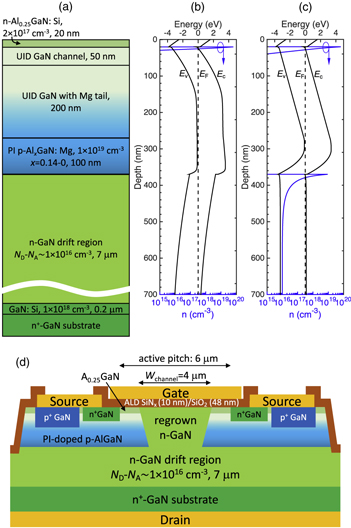
Fig. 1. (Color online) Epitaxial layer structure and device cross-section of the PolarMOS. (a) Designed epitaxial structure for growth by MOCVD. The calculated band diagram and electron concentration along the vertical direction are shown in (b) if Mg acceptors are all active, and in (c) if Mg acceptors are inactive. The Mg profile and Al concentration used in the calculations are taken from the actual values measured by SIMS (see Fig. 2). (d) Schematic device cross-section of the PolarMOS.
Download figure:
Standard image High-resolution imageThe epitaxial layers are grown by MOCVD without interruption. Figure 2 shows the secondary ion mass spectrometry (SIMS) profile of the layers after growth. The peak Al concentration in the graded AlxGaN layer is found to be 14% as designed, and the Mg concentration is ∼5 × 1018 cm−3. Linear grading of the Al concentration is achieved. With the UID GaN "tail" layer, the Mg concentration reduced to ∼1 × 1017 cm−3 before reaching the AlGaN/GaN lateral channel. Using the actual Al and Mg concentrations, the band diagram and electron concentration at zero bias along the vertical direction are calculated. Figure 1(b) shows the calculated results assuming all the Mg acceptors are active, whereas Fig. 1(c) shows the results with all the Mg acceptors inactive. As can be seen from Fig. 1(c), the depletion region does not extend into the n-GaN drift layer if no Mg acceptors are active.

Fig. 2. (Color online) SIMS measurement results as to the impurity concentrations and the Al content along the depth of the epitaxial structure grown by MOCVD.
Download figure:
Standard image High-resolution imageThe device structure of the PolarMOS based on the designed epitaxial layers is shown in Fig. 1(d). As a first step into the device development, a simple metal–insulator–semiconductor gate structure without gate recession is adopted. The vertical n-GaN channel region is designed to be realized by regrowth. The vertical channel forms lateral p-n junctions with the buried p-layer on both sides, resulting in the desired charge-coupling effect and thus reduced surface field for the protection of the gate dielectric.
The fabrication process flow is illustrated in Fig. 3. First, the vertical channel region was defined by dry etching based on BCl3 and Ar, using SiO2 as the mask. The SiO2 mask was patterned by a wet-etch process using buffered oxide etchant (BOE), resulting in a slanted sidewall profile which was then transferred into the sidewall profile of the vertical channel. The slanted sidewall profile is found to have less shadowing effect during the MBE regrowth. After the dry etching, the sample underwent an HCl treatment before being loaded into the MBE system, where the n-GaN vertical channel was selectively regrown using the same SiO2 mask. Subsequently, the SiO2 mask was removed, leaving only the regrown n-GaN in the etched trench. The n+-GaN region for the source contact and p+-GaN region for the body contact were similarly formed by MBE regrowth following similar procedures. After the three regrowth steps, the device was mesa-isolated by dry etching. Non-alloyed source ohmic contacts were then formed by a deposition of Pd/Au on the p+-GaN region, followed by a deposition of Ti/Au on the n+-GaN region. A SiNx/SiO2 (10 nm/48 nm) gate dielectric layer was deposited by atomic layer deposition (ALD), followed by a deposition of Ni/Au as the gate metal. The gate dielectric also served as a passivation layer in ungated regions. Finally, a non-alloyed drain ohmic contact was formed by a deposition of Ti/Al/Au on the back side of the GaN substrate, and contact holes were formed on the source contacts by wet etching using BOE.
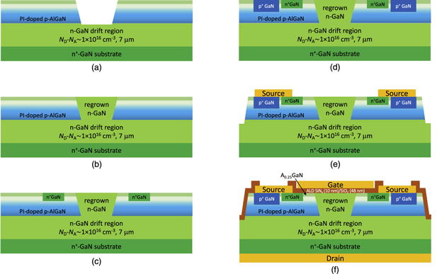
Fig. 3. (Color online) Fabrication process flow of the PolarMOS. (a) Trench formation by dry etching. (b) Vertical n-GaN channel regrowth by MBE. (c) n+-GaN regrowth by MBE for source contact. (d) p+-GaN regrowth by MBE for body contact to the buried p-layer. (e) Metallization for the body ohmic contact (Pd/Au) and source ohmic contact (Ti/Au). (f) Deposition of SiNx/SiO2 (10 nm/48 nm) gate dielectric by ALD, followed by metallization for the gate (Ni/Au) and drain (Ti/Al/Au) electrode.
Download figure:
Standard image High-resolution image3. Structural characterization
The cross-sectional profile of the vertical regrown channel is examined on a test sample. Figure 4(a) shows a scanning electron microscopy (SEM) image of the profile of a vertical channel before the MBE regrowth with a designed width of 3 μm. The sidewall angle is around 45°. Figure 4(b) shows the profile of a vertical channel after the regrowth with the same designed width, taken by high-resolution transmission electron microscopy (HRTEM). Both the horizontal and sidewall regrowth interfaces are indistinguishable under this magnification. The top surface of the regrown channel is flat, but there exist two bumps at each side of the regrown channel. The bumps are due to the undesired growth near the edges of the SiO2 mask, and are found to be largely polycrystalline. There is also a shallow valley at the left side of the right bump. We believe it is due to the shadowing effect of the SiO2 mask and the bump, leading to a reduced atomic flux at the valley during the MBE growth. Figures 4(c)–4(e) show the magnified view of the sidewall regrowth interface on the right side. As can be seen in Fig. 4(c), the regrowth interface can be only vaguely identified near the bottom of the trench, largely from the color contrast between AlGaN and GaN under the TEM imaging. Note that in this particular test sample, the dry etching did not etch through the PI-doped p-AlGaN layer completely. Above the bottom of the trench, the sidewall regrowth interface cannot be identified even with higher magnification, as shown in Figs. 4(d)–4(e). At the highest magnification [Fig. 4(e)], the sidewall regrowth interface appears to have ideal atomic arrangements without visible crystal defects.
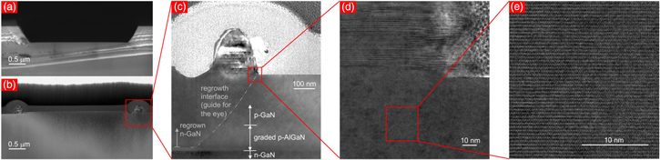
Fig. 4. (Color online) (a) Cross-sectional SEM imaging of the trench sidewall profile after dry etching. The trench has a designed width of 3 μm. (b) HRTEM imaging of the vertical channel after MBE regrowth. Edge bumps due to the undesired growth on the mask sidewall are observed. (c)–(e) HRTEM images with increasing magnifications on the regrowth sidewall interface.
Download figure:
Standard image High-resolution imageFigure 5 shows an SEM image of the cross-section of a fabricated PolarMOS with a viewing angle of 53° from the c axis after adjusting the etching depth of the trench channel based on the aforementioned test sample. Despite the presence of bumps from the regrowth steps, the device has a near-planar surface as designed. The surface morphology of each regrown region is characterized by atomic force microscopy (AFM), as shown in Fig. 6. The regrowth surfaces are decently smooth, all having an rms roughness below 0.7 nm.

Fig. 5. (Color online) SEM image of the cross-section of a fabricated PolarMOS with a viewing angle of 53° from the c axis.
Download figure:
Standard image High-resolution image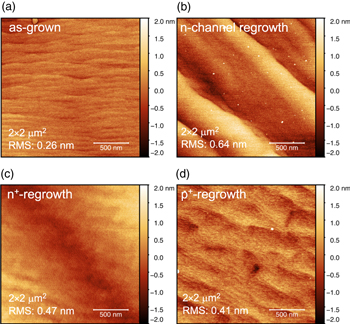
Fig. 6. (Color online) AFM imaging of the surface morphology of the (a) as-grown MOCVD epitaxial structure, (b) regrown n-GaN vertical channel, (c) regrown n+-GaN source contact region, and (d) regrown p+-GaN body contact region.
Download figure:
Standard image High-resolution image4. Electrical characterization
From Hall effect measurements, a 2DEG sheet concentration of 6.7 × 1012 cm−2 and an electron mobility of 1490 cm2/(V · s) is extracted, indicating that the 2DEG channel can indeed be successfully achieved under a Mg background concentration of ∼1 × 1017 cm−3 (see Fig. 2). The contact resistance to the 2DEG is extracted to be 0.19 Ω · mm from transfer length measurements, a figure similar with the typical value we achieved using the same n+-GaN regrowth process by MBE40,41) The contact resistivity to the regrown p+-GaN is measured to be ∼10−4 Ω · cm2. We are unable to measure the contact resistance to the underlying buried p-layer due to the lack of appropriate test structure in this study.
The transfer Id–Vgs characteristics of the PolarMOS under different Vds is shown in Fig. 7. The dimensions of the tested device are shown in Fig. 1(d). Under Vds = 1 V, the PolarMOS has an excellent on–off ratio of ∼109. However, the on–off ratio decreases to less than 102 under Vds = 10 V due to a dramatically increased drain leakage current. Since the gate current remains less than 10−7 mA mm−1, the leakage path is between the source and drain. A significant hysteresis is also observed between different sweeping directions, indicating the presence of trap states in the device structure. The trapping effect will affect the dynamic performance of the present devices. The origin of the trapping requires further investigation, and is beyond the scope of this paper.
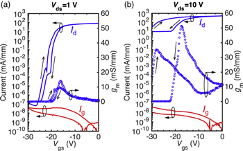
Fig. 7. (Color online) Transfer I–V characteristics of the PolarMOS under (a) Vds = 1 V and (b) Vds = 10 V.
Download figure:
Standard image High-resolution imageFigure 8 shows the Id–Vds output characteristics of the PolarMOS. Decent output current of >500 mA mm−1 is measured under Vds = 10 V. The Ron extracted from the linear region near Vds = 0 V is 11 Ω · mm, corresponding to a specific Ron of 0.66 mΩ · cm2 as normalized by the active pitch width of 6 μm. This value is on par with the best reported specific Ron of 1-kV class vertical GaN transistors.17,20,24,25,27,28) However, there is an increase of drain leakage current beyond a Vds of ∼6 V, and the device cannot be completely turned off at Vds = 10 V, in agreement with the observations from the transfer I–V measurements.
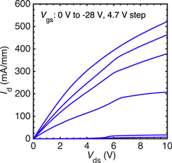
Fig. 8. (Color online) Output I–V characteristics of the PolarMOS.
Download figure:
Standard image High-resolution imageFigure 9(a) shows the 3-terminal breakdown measurement of the PolarMOS under Vgs = −30 V. The drain leakage is found to increase rapidly beyond ∼5 V, while the gate leakage remains at a low level until a hard breakdown behavior at 38 V. This again indicates that the leakage path is between the source and drain. The vertical leakage test through the buried p-layer is performed on a test structure on the same wafer. The test structure does not have the vertical channel, and only has the regrown n+-GaN region for the source ohmic contact. Thus, the vertical current measured in this test structure reflects the leakage current through the buried p-layer. As shown in Fig. 9(a), the measured vertical leakage current closely matches with the drain leakage, indicating that the source-drain leakage is primarily through the buried p-layer. This leads to the speculation that the Mg dopants in the buried p-layer are passivated by the hydrogen present during the MOCVD growth, which is a well-known issue.42) Indeed, there is a high concentration of H, whose profile follows closely with that of the Mg in the buried p-layer, as revealed by the SIMS results (Fig. 2). Upon closer examination of drain current from Fig. 9(a), a punch-through behavior can be identified at around 6 V, where a sharp exponential increase of the current transitions into a gradual linear increase. It is shown in our previous study that similar punch-through behaviors can be verified from simulation, and are well-explained quantitively with an analytical model considering the complete depletion of the buried p-layer.37) In the present epitaxial structure, if the Mg acceptors are completely inactive [see Fig. 1(c)], the negative polarization charge (NA,PI) in the buried PI-doped p-AlGaN layer is balanced with the positive polarization sheet charge at the p-n junction interface arising from the abrupt change of the Al concentration. Using the measured peak Al concentration (xAl) of 14% and the graded AlGaN layer thickness (dp) of 100 nm, NA,PI can be calculated:34)

When the punch-through happens, the applied voltage is supported entirely by the polarization charge in the depleted p-AlGaN layer since the depletion does not extend into the drift layer when the Mg acceptors are inactive. Thus, the punch-through voltage (Vpunch-through) can be calculated with

where εs is the dielectric constant of the buried p-layer. This value is very close to the observed punch-through voltage of 6 V, indicating that the Mg acceptors in the buried p-layer are indeed mostly inactive.

Fig. 9. (Color online) 3-terminal breakdown measurements of the PolarMOS (a) without activation of the buried p-layer and (b) with sidewall activation of the buried p-layer. Dotted line in (a) is the measured vertical leakage current through the buried p-layer using a vertical test structure on the same wafer.
Download figure:
Standard image High-resolution imageAccording to previous studies, the buried p-layer can be thermally activated effectively if exposed with etched sidewall.43,44) Therefore, in another PolarMOS sample, two steps of activation annealing at 725 °C were performed in a N2 ambient for 20 min in an rapid thermal annealing (RTA) system: one after the trench etch and the other after the device-isolation etch. In addition, the sample was annealed in situ in the MBE chamber at 725 °C for 20 min in vacuum before the p+-GaN regrowth, during which the buried p-layer was exposed from the top side as a result of the dry etching before the p+-GaN regrowth. Figure 9(b) shows the 3-terminal breakdown measurement of the PolarMOS that underwent the aforementioned activation steps. The drain leakage current is much reduced within the tested voltage range as compared to the device without the activation, and the leakage current remains low until an abrupt hard breakdown at around 58 V. This suggests that Vpunch-through is improved from 6 to at least 58 V by the activation steps. The increase of Vpunch-through should be attributed to the increase of the active Mg acceptor concentration in the buried p-layer. The exact Vpunch-through value should depend on the width of the mesa structure under a certain annealing condition.44) A comprehensive determination of the Vpunch-through is beyond the scope of this paper. The fact that the breakdown voltage is still lower than 60 V suggests the existence of other breakdown mechanisms than the premature punch-through of the buried p-layer.
To further investigate the breakdown mechanism, the conductive AFM technique was employed for a current mapping of the region near the vertical regrown channel. A test sample was fabricated with only the vertical channel regrowth and the drain ohmic contact, similar to the structure in Fig. 3(b) but with the addition of the drain ohmic contact. A solid conductive tip was used, which stays in contact with top surface of the sample under a constant applied force. Electrically, the tip is grounded. With a bias applied to the sample through the drain ohmic contact at the back side of the substrate, the system measures the local current that passes through the grounded AFM tip and flows vertically through the sample. Figure 10 shows the measurement results. As expected, the topography line scan reveals the bumps at the edge of the regrown channels as a result of the MBE regrowth [Fig. 10(b)]. The current maps are shown in Figs. 10(c) and 10(d) with two different current scales under the same sample bias of 1 V. Referring to the topography map in Fig. 10(a), the current maps allow for the identification of highly conductive paths located at the regrowth bumps. Since the bumps are in contact with the sidewall regrowth interface, the results suggest that the material near the sidewall regrowth interface is much more conductive than at other regions, allowing for a localized vertical leakage path. This path acts like a short in the PolarMOS at reverse bias, resulting in most of the voltage being supported by the gate dielectric alone; thus, the limited breakdown voltage. The high conductivity of the regrowth interface is likely due to the presence of donor-like impurities and/or point defects, which is suggested and partially identified in previous studies on the regrowth of GaN on c-planes.45,46) For semi-polar or non-polar planes, as in the case of the slanted etched sidewalls in the PolarMOS, donor-like impurities such as O may have a higher tendency to get incorporated.47) Perhaps due to this reason, not excluding others, the regrown p-n junctions on non-c-plane surfaces typically show higher leakage current and lower breakdown voltage than those on c-plane surfaces.12,45,48) High concentration of interface charge is also typically found on the etched sidewalls.17,26,30,49) Our results show that the interface donors are present even though apparent structural defects at the sidewall regrowth interface are not visible. Further studies with in situ cleaning and further optimized regrowth processes are required to improve the interface quality for truly functional lateral regrown p-n junctions.

Fig. 10. (Color online) (a) AFM topography of the vertical regrown channels. (b) Line scans of the topography along the dash-dotted lines in (a). (c) Current map in nA scale. (d) Current map in μA scale. The current maps are measured by a grounded conductive AFM tip in contact mode under a constant applied force, with the sample biased at 1 V through the drain ohmic contact on the back of the wafer (i.e. the tip/n-GaN Schottky barrier diode is under reverse bias).
Download figure:
Standard image High-resolution image
Donor-like interface states may also exist at the regrowth interfaces of the regrown n+-GaN and p+-GaN regions.45,46) In the PolarMOS, the high electric field will not reach the n+-GaN and p+-GaN regions unless the buried p-layer becomes fully depleted or the gate loses control over the lateral channel. Thus, the breakdown voltage will not be affected directly by the interface quality of regrown n+ and p+ regions. However, the donor-like interface states between the regrown p+-GaN and the buried p-layer could severely compromise the ohmic behavior of the body contact, causing threshold voltage instability and reduced breakdown voltage due to open-base transistor breakdown. These potential effects, while not observable in the present PolarMOS devices, are worthy of future study.
5. Conclusions
With three steps of selective area regrowth by MBE, GaN PolarMOS is successfully realized with a near-planar surface profile. In the PolarMOS, a lateral heterojunction channel with high-mobility 2DEG is achieved on top of a PI-doped p-AlGaN body layer without growth interruption by MOCVD. The PolarMOS exhibits excellent on-current of >500 mA mm−1 and a specific on-resistance of 0.66 mΩ · cm2. However, the device suffers from a high source-to-drain leakage current due to the early punch-through of the buried p-layer due to the passivation of the Mg acceptors. Through sidewall activations of the buried p-layer, the vertical leakage is significantly suppressed. Subsequently, the breakdown mechanism of the PolarMOS is unveiled from the current maps using the conductive AFM technique, which reveals a highly conductive vertical path along the sidewall interface of the regrown channel despite the absence of apparent structural defects. These findings provide important references towards the advancement of device technologies for high-performance GaN vertical power transistors.
Acknowledgments
This work was supported in part by the ARPA-E SWITCHES program (DE-AR0000454) monitored by Tim Heidel and Isik Kizilyalli, and performed in part at the Cornell Nanoscale Science and Technology Facilities (CNF) sponsored by the NSF NNCI program (ECCS-1542081) and New York State. This work made use of the Cornell Center for Materials Research Shared Facilities, which are supported through the NSF MRSEC program (DMR-1719875).