
Abstract
We investigated the growth of Bi2Te3 thin films on (111) CaF2 and (111) BaF2 substrates by pulsed laser deposition. Stoichiometric Bi2Te3 thin films were grown using targets with excess tellurium. We adopted a combinatorial temperature variation principle, where the growth temperature is monotonically varied during the growth. This growth method is supportive to effectively minimize Te loss in the Bi2Te3 films. We found large differences in growth conditions between Bi2Te3 thin films on the CaF2 and BaF2 substrates. The lattice matched (111) BaF2 substrate is preferred to grow Bi2Te3 for the further development of topological electronics.
Export citation and abstract BibTeX RIS

Content from this work may be used under the terms of the Creative Commons Attribution 4.0 license. Any further distribution of this work must maintain attribution to the author(s) and the title of the work, journal citation and DOI.
The celebrity status of tetradymites 1) stems from their hitherto unparalleled thermoelectric power. 2,3) Yet, the discovery of topological states in these layered materials 4,5) brought renowned attention, particularly in condensed matter physics. These topological states offer an entirely new degree of controllability to potential application devices using Majorana fermion, 6) quantum anomalous Hall effect, 7) and current-spin conversion. 8) To access these exotic phenomena, heterostructures based on topological insulators with atomically flat and abrupt heterointerface are necessary.
Bi2Te3 is known as a typical topological insulator. It is a layered structured material, where Bi and Te layers are stacked upon each other. While there have been reports on the synthesis of Bi2Te3 thin films by molecular beam epitaxy (MBE), 9–13) the potentials of pulsed laser deposition (PLD) technique, which enables the rapid synthesis of thin films under non-equilibrium conditions, 14–16) have not yet been fully investigated. The main culprit for the subpar quality of epitaxially grown Bi2Te3 film roots in the extraordinary high vapor pressure of tellurium, 17–19) which requires that Te loss in the deposited films has to be compensated. Furthermore, an appropriate choice in substrate material and orientation presents an additional hurdle because the lattice mismatch between the substrates and Bi2Te3 may cause in-plane multiple domain orientations. For exploring exotic topological physics occurring in heterostructures based on Bi2Te3, the first challenges are to improve the local crystal quality of Bi2Te3 films and control their domain orientations.
Here we approach this problem by utilizing highly off-stoichiometric targets for the synthesis of Bi2Te3 thin films. Throughout the experiments here, we used a target stoichiometry of Bi:Te = 1:10, which corresponds to more than 6 times the Te required content. For substrate materials, we used CaF2 and BaF2 while using Ar atmosphere in the pressure range of ∼10−3 to 10 Torr. Generally, the higher background pressure results in a lower re-evaporation rate of tellurium. 20,21) If the background gas pressure, however, is too high the deposition process cannot take place. Certainly, other geometric aspects such as the target-substrate distance (60–70 mm) contributes to these limitations.
Under tellurium-rich conditions we were able to increase the synthesis temperature of Bi2Te3 thin films close to the liquefaction point of tellurium (449.5 °C 22)). The key to the effective use of such high growth temperatures is to change the substrate temperature from the initial stage of crystal growth on the substrate to the subsequent steady growth. We increased the substrate temperature monotonically from an initial temperature (T1) up to an endpoint temperature (T2); rather than the ordinary two-step growth, which cannot prevent Te sublimation during heating of the substrate temperature. Such high synthesis temperatures promote the formation of large area domains of Bi2Te3 thin films—an important prerequisite to accessing the unique electronic properties of topological insulators.
The as-received substrates were cut into 5 × 2.5 mm2 pieces and annealed at 500 °C for 10 min under ultra-high vacuum (UHV). The Bi2Te3 films were grown onto (111) CaF2 and (111) BaF2 substrates using a KrF excimer laser (COHERENT COMPEX205) with a wavelength of 248 nm. A rectangular area of the beam was focused onto a 3.4 × 1.0 mm2 spot on the target. The substrate temperature was controlled using a laser (808 nm) heating system and pyrometer (Japan Sensor FTK9 1.95–2.5 μm) assuming black body radiation with an emissivity coefficient of 0.2 of the SiC holder. 23,24) The substrates were bound by silver paste to the SiC holder. The targets were pressed using Bi:Te = 1:10 stoichiometric powder mixture at 40 MPa. The synthesis parameters are listed in Table I. Simultaneously with the start of the Bi2Te3 thin films synthesis, we linearly ramped the substrate temperature from T1 up to T2 with a ramping rate adjusted for 7200 pulses at 20 Hz (1.0 J cm−2). The resulting Bi2Te3 thin film thickness was 150 nm. We systematically varied T1, T2, Ar pressure, laser-repetition rate, and laser fluence.
Table I. Synthesis parameters for the growth of Bi2Te3 thin films by PLD for CaF2 and BaF2 substrates.
| Parameter | Min | Max |
|---|---|---|
| Growth temperature (°C) | 220 | 500 |
| Ar pressure (Torr) | 10−3 | 10 |
| Laser repetition rate (f) | 0.1 Hz | 40 Hz |
The stacking sequence of Bi and Te in Bi2Te3 directly influences the c-axis lattice parameter of Bi2Te3−δ . 11) We determined the c-axis lengths of the Bi2Te3−δ thin films with a precision of ±5 pm, using the Nelson–Riley function. 25) Complementary crystal structure analysis was performed using a high-resolution transmission electron microscope (HRTEM) (JEOL 200F). The morphology of the substrates and Bi2Te3−δ films were characterized using a Bruker Dimension FastScan atomic force microscopy (AFM) with FastScan-A silicon probes.
In Figs. 1(a), 1(b), we show XRD scans of Bi2Te3 film grown on the (111) CaF2 and (111) BaF2 substrates, respectively. The (003), (006), and (0015) diffraction peaks are clearly visible, whereas the (009) and (0012) diffraction peaks are absent due to weak scattering amplitude. Note, the X-ray source used here contains Cu and Kβ
radiation.
and Kβ
radiation.
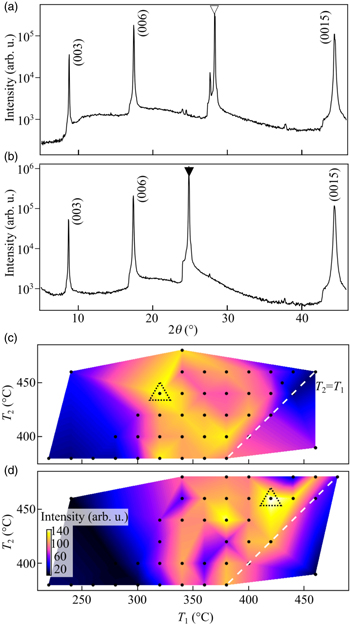
Fig. 1. (Color online) (a) θ–2θ scan of Bi2Te3 thin film on CaF2 substrate grown at T1 = 320 °C and T2 = 440 °C. (b) θ–2θ scan of Bi2Te3 thin film on BaF2 substrate grown at T1 = 420 °C and T2 = 460 °C. In (a) and (b), the triangle marks (111) substrate diffraction position and the Bi2Te3 film (00l) diffraction positions are given. Using (0015) peak intensities for various T1 and T2, we plot figures (c), (d) where (0015) intensities are plotted as a function of T1 and T2, where (c) shows Bi2Te3 films on CaF2 and (d) BaF2, respectively. The optimal growth temperatures are highlighted by dashed triangles. The straight-dashed line corresponds to T1 = T2. Each dot represents individually grown Bi2Te3 film under 3 Torr Ar pressure with laser fluence of 1.0 J cm−2 at a repetition rate of 20 Hz. The film thickness was 150 nm.
Download figure:
Standard image High-resolution imageWe mapped the XRD intensities of (0015) peaks as a function of T1 and T2 while keeping other growth parameters constant. If T1 = T2 [dashed line in Fig. 1(c), 1(d)], Bi2Te3 thin films do form and their crystalline qualities stay below their prospects. Instead, if T1 is lower than T2, the coherent volume associated with the (0015) peak intensity can be significantly enhanced. If T1 < T2, high-quality Bi2Te3 thin films can be grown, particularly within the vicinity of T1 ∼ 320 °C and T2 ∼ 440 °C on the CaF2 substrates [Fig. 1(c)]. However, if T1 is larger than T2, the film quality rapidly deteriorates. All subsequent experiments were conducted at T1 smaller than T2. Yet, the optimum synthesis (in the dashed triangle, Fig. 1) temperatures were markedly different for Bi2Te3 thin films when grown on the (111) BaF2 substrates. In fact, T1 for the optimal growth conditions may differ more than 100 °C between the two substrate materials. The endpoint temperature, however, is independent of the substrate material. We assign the difference in initial temperature T1 to the distinctively different lattice mismatch.
We consistently recorded c-axis lengths from the Bi2Te3 10 (00l) diffraction peaks that are even longer than those determined from bulk samples (30.44 Å 26)). Several reasons might be considered to be accountable for the observed differences. Let us briefly consider Bi2Te3 as an ionic compound with Bi+3 and Te−2. The associated ionic radii 27) are 1.17 Å and 2.21 Å, respectively. Apparently, anti-site defects can be considered to be the primary reason for the observed c-axis length expansion.
In Fig. 2, we show high-resolution scanning transmission electron microscopy (HRSTEM) cross-sectional images of Bi2Te3 on the CaF2 (a) and BaF2 (b) substrates. As Bi2Te3 is built from three individual quintuple layers (QLs) of Te–Bi–Te–Bi–Te, for both substrate materials these QLs were clearly observed. Here, the substrate material has a highly ionic bond character and additional Te layers are not observed. Therefore, the Bi2Te3 phase directly forms on the CaF2 or BaF2.
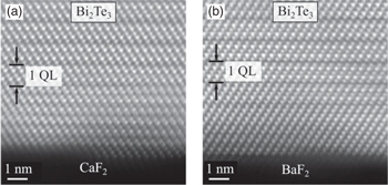
Fig. 2. (a), (b) Cross sectional HRSTEM images taken at the interface region of Bi2Te3 and CaF2 (a) and BaF2 (b) substrates. The growth conditions are as shown in Fig. 1. In (a) and (b), we highlighted one QL of Bi2Te3. The horizontal direction is  . Note, the extreme difference in bonding character between Bi2Te3 (covalent) and halide substrate (ionic) does not allow simultaneous recording of film and substrate using HRSTEM due to extremely different defocussing lengths.
Download figure:
Standard image High-resolution imageWhile such HRSTEM images are of great value to determine the local quality of the Bi2Te3 thin films, it provides little information about the long-range order. Instead, high-resolution XRD (HRXRD) techniques provide a deeper insight. In Fig. 3, we show the HRXRD data for (001)Bi2Te3/(111)CaF2 and (001)Bi2Te3/(111)BaF2. In addition to the diffraction peaks of the substrates, the (003m) diffraction peaks of Bi2Te3 with m = 1...12 are clearly visible. The c-axis value for Bi2Te3/CaF2 (Bi2Te3/BaF2) is 30.613 (30.584) Å which is slightly longer than the bulk value (30.44 Å 26)). Note that additional diffraction peaks, e.g. (015) and (012) Bi2Te3 are visible. Moreover, as the surface tends to oxidize rapidly, polycrystalline diffraction peaks of TeO2 and Bi2O3 were observed (see SI, available online at stacks.iop.org/APEX/15/065502/mmedia). It is worth noting that energy-dispersive X-ray scattering experiments (see SI) revealed no accumulation of either Bi or Te along grain boundaries.
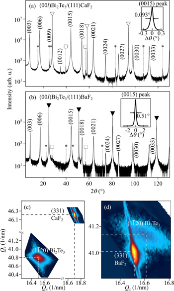
Fig. 3. (Color online) (a), (b) High-resolution 2θ–θ XRD scans of Bi2Te3 films on (111) CaF2 (a) and (111) BaF2 (b) substrates. The measurement was performed by Bruker D8 diffractometer with monochromatic Cu  radiation. Bi2Te3 films were grown at 440 °C using step-and-terrace terminated substrates (see SI). The growth conditions were the same as shown in Fig. 1. The squares (□) denote (012) and (015) planes of Bi2Te3 . The asterisks (*) denote diffraction peaks stemming from TeO2
28) and Bi2O3
29) surface oxides. The open and full triangles denote Bragg positions of CaF2 and BaF2 substrates, respectively. Insets in (a) and (b) show the associated rocking curves of the Bi2Te3 (0015) diffraction peak. (c), (d) Reciprocal space maps in the vicinity of
radiation. Bi2Te3 films were grown at 440 °C using step-and-terrace terminated substrates (see SI). The growth conditions were the same as shown in Fig. 1. The squares (□) denote (012) and (015) planes of Bi2Te3 . The asterisks (*) denote diffraction peaks stemming from TeO2
28) and Bi2O3
29) surface oxides. The open and full triangles denote Bragg positions of CaF2 and BaF2 substrates, respectively. Insets in (a) and (b) show the associated rocking curves of the Bi2Te3 (0015) diffraction peak. (c), (d) Reciprocal space maps in the vicinity of  Bi2Te3 XRD peaks on (111) CaF2 (c) and (111) BaF2 (d), respectively. A two-dimensional Gaussian function was used to determine peak positions in (c) and (d) and the peak positions are indicated by dashed lines.
Download figure:
Standard image High-resolution imageAn established method of revealing the epitaxial relation between film and substrate are using high-resolution reciprocal space maps (HRRSMs). In Figs. 3(c) and 3(d), HRRSMs are shown for Bi2Te3/(111)CaF2 and Bi2Te3/(111)BaF2 in the vicinity of the  diffraction peaks. The
  peak of Bi2Te3 and (331) peak of the substrate are not vertically aligned (
 ) which means the films are fully relaxed. In Table II, the diffraction peak positions and FWHM of (
 ) determined from the HRRSMs are listed. From the Qx
values in Figs. 3(c) and 3(d), we determined the in-plane lattice constants a as 4.395 Å and 4.368 Å for Bi2Te3 on the CaF2 and BaF2 substrates, respectively. The deviation from the bulk value (4.395 Å
26)) is negligible. The coherent volumes, which can be roughly estimated domain sizes, of the thin films on Bi2Te3/BaF2 were estimated as 15 × 15 × 20 nm3 using the Debye–Scherrer formula. In contrast, that of the Bi2Te3 on the CaF2 substrates was significantly larger (80 × 80 × 90 nm3). Remarkably, the lattice mismatch of Bi2Te3 on the CaF2 substrates was 14% whereas it was 0.1% on the BaF2 substrates.
) determined from the HRRSMs are listed. From the Qx
values in Figs. 3(c) and 3(d), we determined the in-plane lattice constants a as 4.395 Å and 4.368 Å for Bi2Te3 on the CaF2 and BaF2 substrates, respectively. The deviation from the bulk value (4.395 Å
26)) is negligible. The coherent volumes, which can be roughly estimated domain sizes, of the thin films on Bi2Te3/BaF2 were estimated as 15 × 15 × 20 nm3 using the Debye–Scherrer formula. In contrast, that of the Bi2Te3 on the CaF2 substrates was significantly larger (80 × 80 × 90 nm3). Remarkably, the lattice mismatch of Bi2Te3 on the CaF2 substrates was 14% whereas it was 0.1% on the BaF2 substrates.
Table II.
 peak positions in the Qx
–Qz
plane and FWHM of the asymmetric HRRSM (unit: nm−1).
peak positions in the Qx
–Qz
plane and FWHM of the asymmetric HRRSM (unit: nm−1).
| Qx | Qz | ΔQx | ΔQz | |
|---|---|---|---|---|
| Bi2Te3/CaF2 | 16.505 | 40.799 | 0.0650 | 0.0847 |
| Bi2Te3/BaF2 | 16.611 | 41.138 | 0.180 | 0.113 |
Bi2Te3 growth is highly susceptible towards the formation of multi-domain orientations.
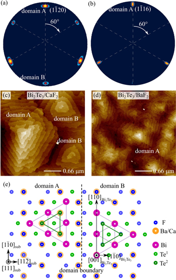
30) An established method to determine a possible domain arrangement of Bi2Te3 thin films on (111) halide substrates are pole figure measurements. We plot the  and
and  Bi2Te3 diffraction peaks of Bi2Te3 on the CaF2 [Fig. 4 (a)] and BaF2 [Fig. 4 (b)] substrates, respectively. If Bi2Te3 were grown as a single domain form, symmetry considerations predict that the
  and
and  diffraction peaks would appear three times for a 360° scan. For Bi2Te3 thin films grown on the (111) CaF2 substrates, however, this is not the case. Instead, the
  diffraction peak appears six times [Fig. 4(a)].
Fig. 4. (Color online) (a), (b) The pole-figure (ϕ–χ) of a Bi2Te3
 and
and  peaks for CaF2 (a) and BaF2 (b) substrates. (c), (d) AFM images of Bi2Te3 thin films grown on (111) CaF2 (c) and (111) BaF2 (d) substrate. The growth conditions are shown in Fig. 1. The details of the substrate treatment are shown in supplemental information. The scan areas in (c) and (d) are 3 × 3 μm2. In (c), two domain orientations are labelled A and B. These orientations are confirmed in (a). In (d) only domain A orientation is visible, as confirmed in (b). (e) Schematic atomic model of a domain boundary. The purple, green, and dark green sphere show Bi, Te1, and Te2 atoms, respectively. The semitransparent blue and orange spheres show F and Ba (Ca) atoms, respectively. Horizontal and vertical axes are parallel to
 ![${\left[11\bar{2}\right]}_{\mathrm{sub}}$](https://content.cld.iop.org/journals/1882-0786/15/6/065502/revision2/apexac6e27ieqn17.gif) and
and ![${\left[1\bar{1}0\right]}_{\mathrm{sub}}$](https://content.cld.iop.org/journals/1882-0786/15/6/065502/revision2/apexac6e27ieqn18.gif) for substrate and
for substrate and ![${\left[1\bar{1}0\right]}_{{\mathrm{Bi}}_{2}{\mathrm{Te}}_{3}}$](https://content.cld.iop.org/journals/1882-0786/15/6/065502/revision2/apexac6e27ieqn19.gif) and
and ![${\left[110\right]}_{{\mathrm{Bi}}_{2}{\mathrm{Te}}_{3}}$](https://content.cld.iop.org/journals/1882-0786/15/6/065502/revision2/apexac6e27ieqn20.gif) for Bi2Te3. Under proper growth condition, Bi2Te3 single crystals were found to grow in two preferential orientations with triangle crystal edges aligned to the [1
for Bi2Te3. Under proper growth condition, Bi2Te3 single crystals were found to grow in two preferential orientations with triangle crystal edges aligned to the [1 0] direction of the CaF2 or BaF2 substrates. Between domains A and B, the stacking sequence differed by 60°.
Download figure:
Standard image High-resolution image
Each peak position is separated precisely by 60° and the absolute intensities of these  diffraction peaks systematically recover every 120°. We conclude that there are two domains which are rotated by 60° to each other. Second, there is a dominant domain as judged by the XRD intensities. Remarkably, for Bi2Te3 films grown on the (111) BaF2 substrates, the
  diffraction peaks repetition was as expected (three times). Moreover, the absolute intensities of these three diffraction peaks did not vary. Consequently, for Bi2Te3 films grown on the (111) BaF2 substrates, single-domain orientation was possible. We note that the single-domain orientation of Bi2Te3 on the BaF2 substrates grown by MBE has been reported.
31) Using the information from the HRRSM (Fig. 3) and the pole-figure (Fig. 4), the epitaxial relation can be written as follows:
diffraction peaks repetition was as expected (three times). Moreover, the absolute intensities of these three diffraction peaks did not vary. Consequently, for Bi2Te3 films grown on the (111) BaF2 substrates, single-domain orientation was possible. We note that the single-domain orientation of Bi2Te3 on the BaF2 substrates grown by MBE has been reported.
31) Using the information from the HRRSM (Fig. 3) and the pole-figure (Fig. 4), the epitaxial relation can be written as follows:
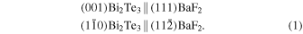
Figure 4(e) illustrates the epitaxial relation [Eq. (1)] for domain A. In addition, the formation of a twin domain with a 60° rotation is also depicted in Fig. 4(e) where a domain boundary is shown along the [110] direction.
In real space [Fig. 4(e)], a 60° domain rotation gives rise to a non-commutative sequence of the stacking order in Bi2Te3. This is also commonly observed for Bi2Te3 films grown on covalent substrates, i.e. (111) Si or (111) Ge, 31) where an additional layer of Te is sandwiched between substrate and Bi2Te3 film. The coherent crystalline volume picked up by XRD [Figs. 3(c), 3(d) and Figs. 4(a), 4(b)] can be directly observed using AFM [Fig. 4(c), 4(d)]. A rough estimation of the lateral dimensions of Bi2Te3 domains provides 1.5 × 1.5 μm2 for the (111) CaF2 substrates, whereas 0.5 × 0.5 μm2 for the (111) BaF2 substrates. For a lattice-mismatched substrate material, e.g. (001) Al2O3 32) or (111) Si, 33) it was reported that embedding a sandwich layer of Bi or Te significantly minimizes the twinning tendencies of Bi2Te3 film. Our results for the lattice-matched substrate [(111) BaF2] indicate that, even with direct synthesis on the substrate, twin formation can be significantly suppressed. To use these films for the study of topological phenomena, we need to increase the Bi2Te3 domain size because carrier scattering at domain boundaries may affect the transport properties.
In conclusion, we found that over-stoichiometric Bi2Te3 target, high-Ar pressure, and optimized growth temperature sequence are prerequisites to synthesize stoichiometric Bi2Te3 thin films by PLD. Furthermore, lattice matching between Bi2Te3 film and substrate is vital for the formation of single oriented Bi2Te3 films. Using a monotonically increasing substrate temperature during the deposition process at high Ar pressures, thin films with nearly stoichiometric Bi2Te3 composition and single-oriented domains were grown on the (111) BaF2 substrates from excessively (1:10) Te rich targets. Our HRSTEM data did not reveal the existence of an interface Te layer between Bi2Te3 films and substrate. The lattice matched (111) BaF2 substrate is preferred to grow Bi2Te3 for the further development of topological electronics.
Acknowledgments
The authors acknowledge Takayuki Ikeda for his support in conducting STEM measurements. This work was partly supported by JSPS KAKENHI Grant No. 20H05670 and 20H02563.