
Abstract
We report the characterization of a N-polar InGaN layer deposited by metalorganic vapor-phase epitaxy on a ScAlMgO4(0001) (SAM) substrate without a low-temperature buffer layer. The InGaN layer was tensile-strained, and its stoichiometry corresponded to In0.13Ga0.87N. We also present the microstructural observation of the InGaN/SAM interface via integrated differential phase contrast-scanning transmission electron microscopy. The results show that the interface between N-polar InGaN and SAM occurs between the O atoms of the O–Sc SAM surface and the (Ga,In) atoms of InGaN.
Export citation and abstract BibTeX RIS

Content from this work may be used under the terms of the Creative Commons Attribution 4.0 license. Any further distribution of this work must maintain attribution to the author(s) and the title of the work, journal citation and DOI.
Due to its optical versatility, InGaN has played a crucial role in recent developments of III-nitride optoelectronic devices. Light-emitting devices covering the entire visible spectrum can be fabricated by modifying the metallic stoichiometry of InGaN and thus tuning its bandgap. 1–4) This property has led to the fabrication of RGB LEDs and the eventual commercial fabrication of InGaN-based RGB displays. 5) The same tuning feature benefits photoabsorption devices such as solar cells and photocatalysts, which can be designed to absorb most solar light improving their energy conversion efficiency. 6,7)
However, several issues compromising the quality of the material arise as the In-content in InGaN increases. High In-content InGaN quantum wells (QWs) suffer from low growth temperature, 8,9) a high strain due to their lattice mismatch with GaN (template commonly used to grow InGaN-based devices), and an enhanced quantum confined Stark effect (QCSE). 10–12) The first two issues directly impact the crystalline quality of InGaN, 13,14) while the QCSE spatially separates electrons and holes in QWs. The internal quantum efficiency drop observed in InGaN-based LEDs as their emission wavelength is changed from the blue to the green or red regions is mainly due to these issues although several techniques have been helpful to mitigate them. The growth temperature of InGaN QWs has been increased by modifying the flow-channel of the metalorganic vapor-phase epitaxy (MOVPE) reactor 15) and optimizing its growth rate. 16) The use of Al(Ga)N strain-compensating barriers has increased the crystalline quality of InGaN QWs and improved the external quantum efficiency of InGaN-based LEDs. 17–19)
Two lattice-matched substrates have been used to reduce the lattice mismatch between InGaN and its template, which generates dislocations and mechanical strain: ZnO and ScAlMgO4 (SAM). The lattice geometry of ZnO matches In0.18Ga0.82N, and the growth of epitaxial In0.25Ga0.75N on ZnO has been achieved with pulsed laser deposition (PLD). 20) In the case of the SAM substrate, the lattice size matches In0.17Ga0.83N and has a mismatch of only 1.8% with GaN. 21) Epitaxial GaN and InGaN depositions on SAM have already been demonstrated with PLD, halide vapor-phase epitaxy, and MOVPE. 21–25)
Recent research on InGaN-based devices on SAM has used GaN as a template, 26,27) not fully lattice-matched to SAM but whose epitaxial process is better controlled. The direct epitaxy of InGaN on SAM by MOVPE has resulted in poor crystalline quality, although it has been improved via a low-temperature (LT) InGaN buffer layer. The FWHM of the InGaN(0002) X-ray diffraction (XRD) peak achieved in this case was 0.7°. 21) The use of an LT buffer layer has been deemed necessary in the heteroepitaxial growth of materials with considerable dissimilar lattice structures, e.g., III-nitrides on Al2O3. However, it is not necessary for lattice-matched substrates, as demonstrated by the successful direct growth of high-quality GaN on SAM. 28) The amorphous nature and growth conditions of LT buffer layers may enhance defect generation and propagation on subsequent grown layers; thus, their exclusion should promote a better crystalline quality when not structurally necessary.
Another general challenge in the growth of III-nitride materials is the control of their polarity along the c-axis. During the growth of GaN by PLD on SAM, annealing the substrate in a hydrogen or ambient atmosphere leads to a Ga- or N-polarity, respectively. 29) N-polar III-nitrides find applications in the fabrication of specialized transistors 30,31) and facilitate the incorporation of In into InGaN, which is beneficial for the fabrication of high In-content QWs. 32) Here, we characterized the crystalline and interfacial microstructural properties of N-polar InGaN grown on SAM without an LT buffer layer. Our results demonstrate the possibility of depositing directly high-quality N-polar InGaN on SAM with a crystalline quality comparable to Ga-polar InGaN layers deposited using LT buffer layers on SAM substrates.
The InGaN layer was directly grown by MOVPE on a SAM(0001) substrate (Fukuda Crystal Laboratory) without any LT buffer layer and using a customized single-wafer horizontal reactor. 15) The substrate had a thickness of 500 μm and a 0.2° miscut angle towards its m-axis. Preceding the InGaN deposition, the SAM substrate was thermally cleaned in the MOVPE reactor at 1000 °C for 5 min in H2. Afterward, the atmosphere was changed to N2 and the temperature was decreased to 833 °C. Once the temperature stabilized, the InGaN growth process was done using N2 as the carrier gas and trimethylgallium (TMGa), trimethylindium (TMIn), and NH3 as Ga, In, and N precursors. The V/III and TMIn/(TMGa + TMIn) vapor ratios during the InGaN growth were 10 000 and 0.63, respectively. The final thickness of the InGaN layer was approximately 220 nm. Figure 1 shows the InGaN surface via scanning electron microscopy (SEM) and atomic force microscopy (AFM). The SEM image shows no formation of large V-pits. However, the topographic image by AFM revealed the formation of hexagonal hillocks, a feature typical of N-polar InGaN or GaN, 33,34) rather than an atomically flat surface. The RMS roughness of the layer was 10.7 nm over a 10 × 10 μm2 area, comparable to the value of 12.0 nm reported for InGaN grown on Ga-polar GaN/SAM. 28)

Fig. 1. (Color online) (a) SEM and (b) AFM micrographs of the InGaN grown directly on a ScAlMgO4 substrate.
Download figure:
Standard image High-resolution imageThe analysis of the crystalline quality and structural parameters of the InGaN layer was done using XRD. Figure 2 shows the InGaN( ) and InGaN(10
 ) rocking curves (RCs) as well as the reciprocal space mappings (RSMs) of SAM(10
 ) and InGaN(10
 ). The FWHM of the InGaN(
 ) in our sample was 720 arcsec (=0.2°), narrower than the 0.7° and 0.83° reported for InGaN grown on SAM with an LT buffer layer
21) and InGaN grown on Ga-polar GaN/SAM,
28) while the FWHM of the InGaN(10
) in our sample was 720 arcsec (=0.2°), narrower than the 0.7° and 0.83° reported for InGaN grown on SAM with an LT buffer layer
21) and InGaN grown on Ga-polar GaN/SAM,
28) while the FWHM of the InGaN(10 ) was 1612 arcsec. The lattice parameters obtained for InGaN from the RSM were a = 3.25 Å and c = 5.24 Å, corresponding to the lattice parameters of a tensile-strained In0.13Ga0.87N layer. The RSMs also show that the peaks of InGaN and SAM are not entirely aligned vertically. The lattice parameters obtained for the SAM substrate are a = 3.26 Å and c = 25.12 Å, slightly different from the values previously reported of a = 3.249 Å and c = 25.195 Å.
35) However, recent studies show that the RC peak positions of SAM present variations as the measurement position in the substrate is changed;
36) therefore, an accurate determination of the SAM lattice parameters from XRD measurements requires further confirmation.
) was 1612 arcsec. The lattice parameters obtained for InGaN from the RSM were a = 3.25 Å and c = 5.24 Å, corresponding to the lattice parameters of a tensile-strained In0.13Ga0.87N layer. The RSMs also show that the peaks of InGaN and SAM are not entirely aligned vertically. The lattice parameters obtained for the SAM substrate are a = 3.26 Å and c = 25.12 Å, slightly different from the values previously reported of a = 3.249 Å and c = 25.195 Å.
35) However, recent studies show that the RC peak positions of SAM present variations as the measurement position in the substrate is changed;
36) therefore, an accurate determination of the SAM lattice parameters from XRD measurements requires further confirmation.
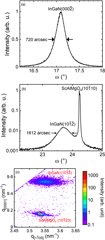
Fig. 2. (Color online) XRD RC of (a) InGaN( ) and (b) InGaN(10
 ) grown on a ScAlMgO4(0001) substrate. (c) RSMs of ScAlMgO4(10
 ) and InGaN(10
 ).
).
Download figure:
Standard image High-resolution imageTo corroborate the In content of the InGaN layer, we performed an elemental composition analysis by transmission electron microscopy (TEM) energy-dispersive X-ray spectroscopy (EDS). The TEM lamella sample was prepared using a dual-beam gallium focused ion-beam/SEM system. Before the lamella preparation, the InGaN surface was covered with electron-deposited carbon and platinum, followed by ion-deposited platinum as protective layers. The TEM system used in the measurements was a double Cs-corrected Titan Themis Z (Cs, spherical aberration; Thermo Fisher Scientific) operating at 300 kV. Figures 3(b) and 3(c) show the quantification of the In content of the layer in the parallel and perpendicular directions to the InGaN surface, respectively, from the regions indicated in the high-angle annular dark-field (HAADF)-scanning TEM (STEM) image shown in Fig. 3(a). Regardless of the local fluctuations of In content observed in both profiles, their average resulted in 11 at%, slightly lower than the 13 at% calculated from the lattice parameters of the InGaN RSM. The lower In content obtained in the EDS analyses can be explained by the Ga implantation suffered by the TEM lamella during its fabrication, 37) which would decrease the In/(Ga + In) ratio measured. The appearance of a single peak in the RSM of InGaN and the absence of significant trends in the In content profiles demonstrate that the InGaN layer maintained its structure and average composition despite its considerable thickness.
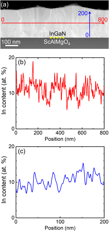
Fig. 3. (Color online) (a) HAADF-STEM micrograph of the InGaN layer showing the regions used for EDS analysis. (b) and (c) show the In content profiles along the red and blue lines displayed in (a), respectively.
Download figure:
Standard image High-resolution imageBased on the FWHM values obtained for the symmetric and asymmetric RCs, the estimated 38) screw and edge dislocation densities of the sample were 1.0 × 109 cm−2 and 2.6 × 1010 cm−2, respectively. The large edge dislocation density cannot be composed only of dislocations caused by the lattice mismatch between the InGaN layer and the SAM substrate because they are nearly lattice-matched. Figure 1(b) shows the presence of hexagonal hillocks on the InGaN surface due to the vast number of uncoalesced grains formed at different nucleation sites. The hillocks density was 1.3 × 109 cm−2, and because the boundaries of each hillock likely generate more than a single edge dislocation, we believe that the hillocks contribute extensively to increasing the InGaN edge dislocation density. Likewise, the high density of hexagonal hillocks may also increase the InGaN screw dislocation density. 39,40)
The different types of threading dislocations were directly observed with TEM. Figure 4 presents the regular and dark-field cross-sectional TEM micrographs of the InGaN/SAM interface. The a- and (a + c)-type threading dislocations observed in Fig. 4(b) show the presence of extended faults parallel to the InGaN -c planes. Figure 4(c) shows that most of the c- and (a + c)-type threading dislocations are generated at the interface with SAM. Nonetheless, not all these dislocations are perpendicular to the InGaN c-plane; therefore, it is expected that increasing the thickness of the InGaN layer contributes to the merging of mixed dislocations, which would improve the crystalline quality of InGaN.
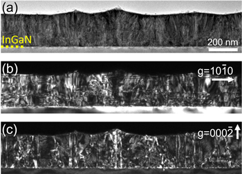
Fig. 4. (Color online) (a) Cross-sectional TEM image of the InGaN/ScAlMgO4 interface and corresponding dark-field images with (b) g = 10 0 and (c) g = 000
 (b) shows the a- and (a + c)-type threading dislocations, and (c) the c- and (a + c)-type threading dislocations.
Download figure:
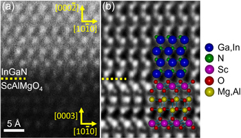
Standard image High-resolution imageOne advantage of using an epitaxial growth process that does not require an LT buffer layer is that there should be a clear interface between InGaN and SAM. Previous studies have presented several possibilities about the SAM surfaces that are most likely to get in direct contact with InGaN or GaN and even how these surfaces influence the polarity of these materials. 29,41) Essentially, there are two possible SAM surface terminations in its polar direction based on the crystallographic structure: the (Al, Mg)-O surface from the wurtzite-like part of SAM and the O–Sc surface from the rocksalt part of SAM. High-resolution HAADF-STEM allows the direct observation of atomic columns, which is helpful to establish the general orientation of a crystal; however, it is limited in resolving the position of columns of light atoms like O or N. In c-axis oriented InGaN, the relative position of the N columns regarding the metallic ones determines its polarity.
To confirm the interfacial structure and polarity of the InGaN/SAM sample unequivocally, we next used integrated differential phase contrast (iDPC)-STEM.
42,43) With this method, two simultaneous images are obtained: one high-resolution HAADF-STEM image where the contrast is mainly generated by the atomic weight of the elements (Z-contrast) forming a column and an iDPC-STEM image where the contrast is enhanced for light elements. These observations were also performed in the double Cs-corrected Titan Themis Z TEM, operated at 300 kV, with a probe current of 70 pA, a semi-convergence angle of 30 mrad, a pixel size of 13 pm, and a dwell time of 20 μs/pixel. The collection angles for the HAADF-STEM and iDPC-STEM were 31–187 mrad and 7–29 mrad, respectively. The detector used for the iDPC imaging was a four-quadrant DF4 detector with a high-pass filter to reduce the low-frequency noise in the images. The area observed in both images is the same, which permits the correlation of the position of heavy elements from the HAADF-STEM image into the iDPC-STEM image. Figure 5(a) shows the InGaN/SAM interface by HAADF-STEM, and Fig. 5(b) the corresponding iDPC-STEM image. These micrographs confirm that InGaN and SAM kept an epitaxial relationship with the InGaN  ∣∣SAM
∣∣SAM  and InGaN[
 ]∣∣SAM[
 ] symmetry constraints. We found the positions of the metal columns in the iDPC-STEM image based on the Z-contrast of the HAADF-STEM micrograph and then determined the positions of the N columns in InGaN and O columns in SAM. This feature permitted us to correctly overlap the crystallographic projections of InGaN and SAM at their interface, as shown in Fig. 5(b).
Fig. 5. (Color online) (a) HAADF-STEM micrograph of the InGaN/ScAlMgO4 interface and (b) corresponding iDPC-STEM image. The crystallographic projections of InGaN and ScAlMgO4 oriented in their respective directions are overlapped in (b) for reference.
Download figure:
Standard image High-resolution image
The polarity of InGaN was N-polar, which explains the topographic features of the sample. In the case of N-polar GaN, the O–Sc SAM surface termination promotes N-polarity. 29) That surface termination is achieved via thermal annealing of the SAM substrate in an ambient atmosphere because it is expected that the stable surface terminations of sliced SAM substrates are the (Al, Mg)-O surfaces. 44) In our case, we believe that the high growth temperature and initial flux of metalorganic gases in the MOVPE growth process should emulate the atmospheric oxidation of the SAM substrate and expose its O–Sc surface, which induced the N-polarity in InGaN. The extended faults observed in Fig. 4(b) did not generate inversion domains. Besides, no polarity conversion was observed, neither parallel nor perpendicular to the growth direction, indicating that the N-polarity was preserved in the entire layer. Our results demonstrate that the N-polar InGaN/SAM interface is formed by the (Ga, In) atoms of InGaN bound to the O atoms in the O–Sc SAM surface. The microstructural observation of the interface shows a one-to-one correspondence between the interfacial atoms. However, as demonstrated by the XRD measurements, there is a slight difference in the size of the a lattice parameters of InGaN and SAM, though it is noticeable only in "bulk" measurements rather than microstructural observations.
In summary, we demonstrate the possibility of growing N-polar InGaN on a SAM substrate without the need for a LT buffer layer. We observed that both materials kept an epitaxial relationship with the InGaN  ∣∣SAM
∣∣SAM  and InGaN[
 ]∣∣SAM[
 ] symmetry constraints. Besides, the InGaN layer stoichiometry corresponded to In0.13Ga0.87N and the FWHM of the InGaN(
 ) XRD RC peak was only 720 arcsec, therefore indicating better crystalline quality than metal-polar InGaN/SAM structures grown with LT buffer layers. Finally, the microstructural observation of the InGaN/SAM interface showed that the interface occurs between the O atoms in the O–Sc SAM surface and (Ga, In) atoms of the InGaN layer, similar to the interface predicted for N-polar GaN deposited on a SAM substrate.
Acknowledgments
This work was financially supported by King Abdullah University of Science and Technology (KAUST) (BAS/1/1676-01-01).