
Abstract
The lateral growth of Si-quantum dots (QDs) on line-patterned SiO2 from the thermal decomposition of pure monosilane (SiH4) has been systematically examined. We confirmed that the Si-QDs diameter in the line direction of the SiO2 patterns has the same growth rate as the SiO2 thin film surface without the line patterns. Moreover, it has been found that in the growth of Si-QDs in the width direction, a surface migration of Si precursors adsorbed from space regions could contribute to dots growth on line-patterned SiO2, which results in an elliptical growth. Furthermore, we have demonstrated a one-dimensional arrangement of highly dense-elliptical shaped Si-QDs with high uniformity in size by controlling line width, CVD time, and temperature.
Export citation and abstract BibTeX RIS
1. Introduction
Si-nanocrystals with a size below ∼15 nm embedded in SiO2 network have attracted a great deal of interest as quantum dots and their application to floating gate MOS memories, 1–6) LEDs, 7–13) electron field emission devices, 14–16) and Si-based quantum computation. 17–24) Nevertheless, how to control QD size, density, uniformity in size, and position remain research issues in obtaining reliable device operation. Thus, in our previous work, we have demonstrated the fabrication of Si-QDs on ultrathin SiO2 by controlling the early stages of low-pressure CVD (LPCVD) using a monosilane (SiH4) gas. 25) Additionally, we reported that surface OH bonds serve as reactive sites for SiH4-LPCVD, which results in nucleation control. Consequently, hydroxylation of the SiO2 surface with dipping in the dilute hydrogen fluoric (HF) acid solutions is very effective in increasing areal dot density above ∼1011 cm−2. 26) Furthermore, we found that an increase in the number of OH bonds enables us to enhance dot size uniformity. 26) More recently, we successfully presented selective growth of Si-QDs by spatially controlled preparation of the reactive sites on the SiO2 surface. 27) However, enhancement of size uniformity remains a matter of research. To overcome this drawback, namely, to improve size uniformity, the diffusion length of the Si precursor must be considered. For the case of SiH4-LPCVD, the average surface migration length of Si precursors was determined to be ∼48 nm, which is extracted from the correlation between areal dot density and the distance from the edge of a line with OH bonds. 28) Thus, in this work, we extended our research work to evaluate the growth mechanism of Si-QDs on 50- and 20 nm width SiO2 line patterns. Compared with the results published in Ref. 29 more in-depth discussions regarding the lateral growth mechanism of Si-QDs are given in this paper.
2. Experimental methods
After the conventional wet-chemical cleaning step, a ∼3.0 nm thick SiO2 layer was grown on an n-type Si(100) substrate at 1000 °C in dry O2. Afterward, SiO2 line and space patterns were fabricated by electron beam lithography with a positive resist ZEP520A diluted with anisole at a dose amount of 120 μCcm−2; subsequently, dry etching was performed using tetrafluoromethane (CF4) gas, where input power of RF, gas flow rate, pressure, and etching time were 70 W, 80 sccm, 2.0 Pa, and 70 s, respectively. In this experiment, the line width was set from 20 to 50 nm and the space width was kept constant at 50 nm. To form an OH-terminated SiO2 line and to make an H-terminated bare Si surface, the samples were shortly dipped into 0.1% HF acid solution. Subsequently, by annealing at 800 °C in O2 ambience, the H-terminated Si surface was oxidized despite the Si-OH bond being stable at 800 °C. 28) Afterward, SiH4-LPCVD was performed at 580 °C. The formation of Si-QDs was confirmed via scanning electron microscopy (SEM).
3. Results and discussion
Figure 1 shows SEM images of 50 nm width SiO2 line patterns taken before and after SiH4-LPCVD at 580 °C. Before the SiH4-LPCVD, we confirmed the formation of well-defined ∼50 nm width SiO2 line patterns [Fig. 1(a)]. When the SiH4-LPCVD was conducted for 30 s, the formation of Si-QDs with an areal density as high as ∼2.6 × 1011 cm−2 was observable on the SiO2 line patterns, whereas the areal dots density was as low as ∼109 cm−2 on the space regions [Fig. 1(b)]. This result indicates highly selective nucleation on OH-terminated SiO2 line surfaces. As the CVD time increases from 30 to 60 and 100 s [Figs. 1(c) and 1(d)], it is clear that the Si-QDs increase significantly; however, the areal dot densities decrease down to 2.2 and 1.9 × 1011 cm−2 on the SiO2 line patterns and SiO2 thin film, respectively. Based on these SEM images, areal dot density on the lines and thin film were summarized, as shown in Fig. 1(e). Obviously, the areal dot density on the ∼50 nm width lines linearly decreased with an increase in the CVD time, which is almost the same as that on SiO2 thin film. This result indicates that after nuclei formation, no new nucleation takes place only coalescence growth. Note that for the 50 nm width SiO2 line patterns, one-dimensional arrangement growth of the Si-QDs is hardly observed even when the CVD time is increased. To clarify the difference in lateral growth of the Si-QDs, dot size distribution, namely, the diameter of the dot in the line and width directions of the pattern was evaluated, as shown in Fig. 2. Obviously, no significant change exists in the dot diameter when compared with the dot diameter in the line and width directions of the SiO2 patterns. Additionally, we confirmed that the dot height evaluated via atomic force microscopy is close to the diameter evaluated via SEM. This result indicates that the dot shape is hemispherical. According to these results, the average diameter in the line and width directions of the SiO2 patterns were summarized as a function of CVD time, as shown in Fig. 3, where the average diameter of dot was estimated by fitting a log–normal function to dot diameter distribution. It is found that as the CVD time increases, the diameter of the dots grows similarly in both the line and width directions. Note that on 20 nm width SiO2 line patterns, which are shorter than the surface migration length of Si precursors, Si-QDs become elliptical. Figure 4 shows the size distributions of Si-QDs formed on 20 nm width SiO2 line patterns evaluated from SEM images. When the CVD time is for 30 and 60 s, there is no significant change in the average diameter in the line and width directions of the SiO2 patterns. Further increasing the CVD time up to 100 s and above, the average diameter in the line width direction of the SiO2 pattern increased when compared with that in the line direction (Fig. 5), where the growth rate in the width direction for 150 s was ∼2 times faster than that in the line direction. This result indicates that line widths shorter than the surface migration length of the Si precursors result in elliptical shapes of dots. Therefore, the self-assembling formation of Si-QDs on SiO2 line patterns can be considered as shown in Fig. 6. For the case of 50 nm width SiO2 line patterns, because the SiO2 line width is comparable with the average surface migration length of Si precursors (∼48 nm), 28) precursors migrating from space regions contribute little to the dot growth on lines [Figs. 6(a) and 6(a')]. Consequently, Si-QDs on the 50 nm line pattern were hemispherical. Alternatively, in the case of a 20 nm width line pattern, the incorporation of precursors from space regions into the nuclei on the line becomes significant [Figs. 6(b) and 6(b')], namely, QDs growth in the line width direction is promoted by loading effect. 30) This result indicates that, by controlling the loading effect, size uniformity can be controlled. Due to the loading effect, we have successfully demonstrated a one-dimensional arrangement of Si-QDs with high uniformity in size, as shown in Fig. 7. When comparing the full-width at half-maximum (FWHM) values of the size distributions evaluated from SEM images taken after the formation of Si-QDs on the ∼25 nm width SiO2 line patterns at 580 °C and 600 °C for 150 s, no significant change in the FWHM values in the line direction is observed. Note that the FWHM values in the line width direction are ∼9.0, and ∼14.7 nm at 600 °C and 580 °C, respectively, which indicates that one-dimensional Si-QDs with high uniformity have been achieved when the Si-QDs formed on the ∼25 nm width SiO2 line patterns at 600 °C.

Fig. 1. Top view of SEM images taken (a) before and (b) after SiH4-LPCVD for 30, (c) 60, and (d) 100 s and (e) areal dot density on SiO2 line patterns as a function of CVD time. A typical SEM image of the Si-QDs formed on SiO2 thin film without line patterns for 60 s shown in the inset in (e), and areal dot density as a function of the CVD time is also shown as a reference.
Download figure:
Standard image High-resolution image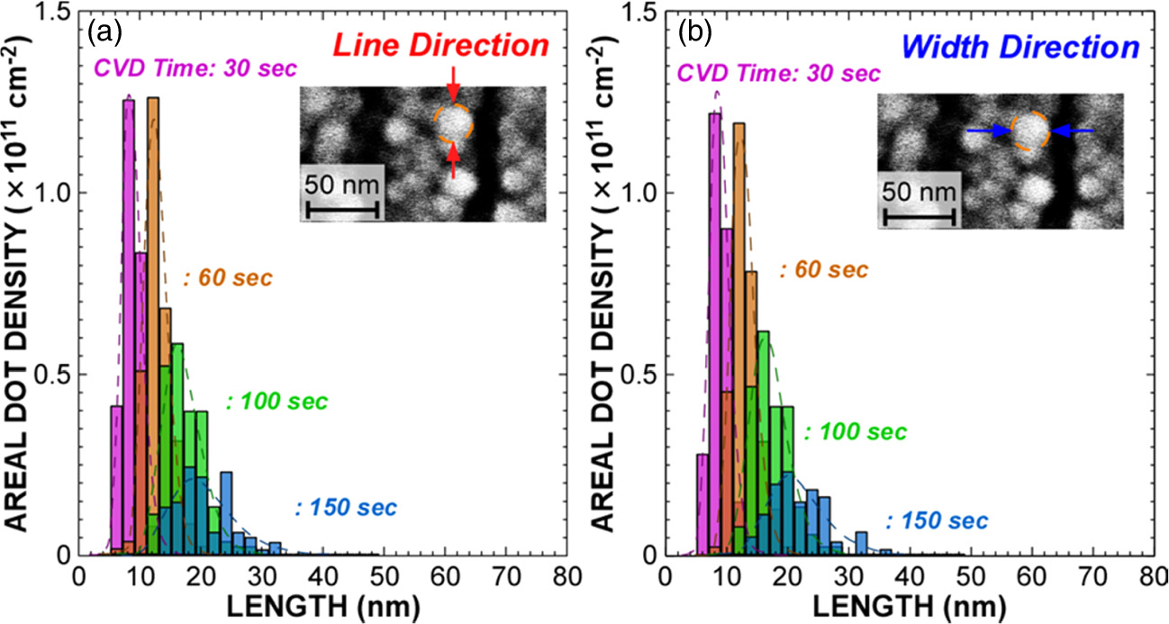
Fig. 2. Size distributions in (a) line direction and (b) width direction of the Si-QDs formed on the 50 nm width SiO2 line patterns at 580 °C for 30, 60, 100, and 150 evaluated from the SEM images. Typical SEM images of the Si-QDs on the SiO2 line formed at 580 °C for 100 s are also shown in the inset.
Download figure:
Standard image High-resolution image
Fig. 3. Average length of the Si-QDs formed on the 50 nm width SiO2 line patterns in line and width directions and areal dot density on the line as a function of CVD time.
Download figure:
Standard image High-resolution image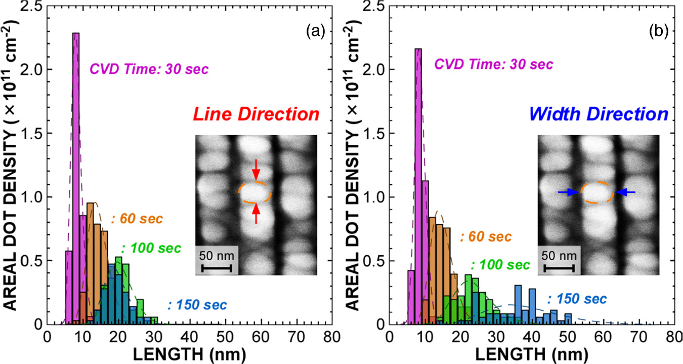
Fig. 4. Size distributions in (a) line and (b) width direction of the Si-QDs formed on the 20 nm width SiO2 line patterns at 580 °C for 30, 60, 100, and 150 s evaluated from the SEM images. Typical SEM images of the Si-QDs on the SiO2 line formed at 580 °C for 150 s are also shown in the inset.
Download figure:
Standard image High-resolution image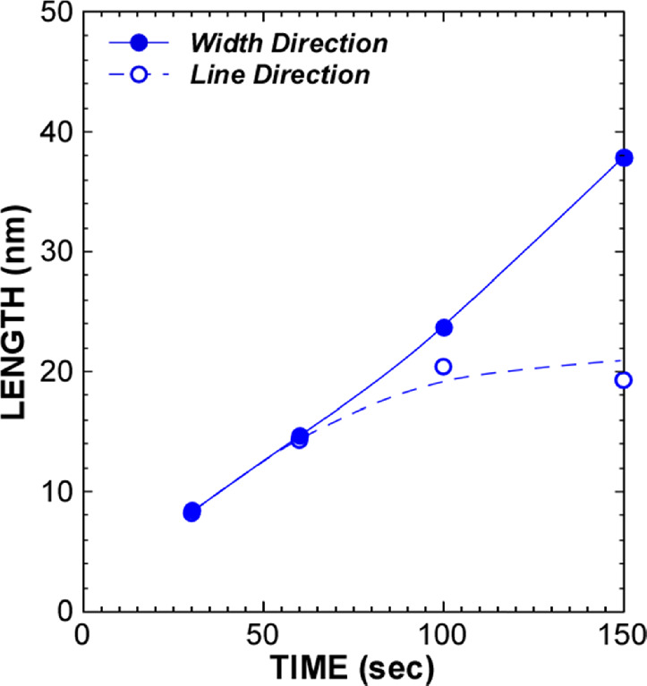
Fig. 5. Average length of the Si-QDs formed on the 20 nm width SiO2 line patterns in line and width directions as a function of CVD time.
Download figure:
Standard image High-resolution image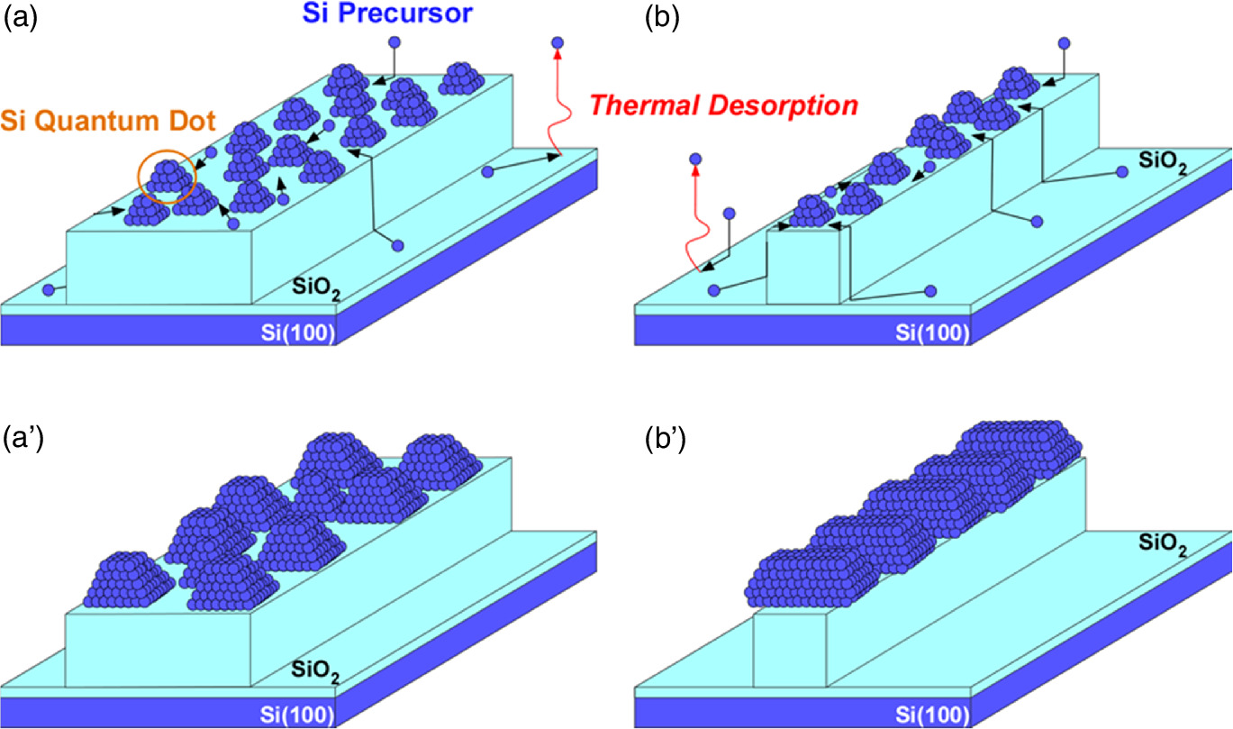
Fig. 6. Schematic illustration of the self-assembling formation of the Si-QDs on [(a) and (a')] 50 nm width SiO2 line patterns and [(b) and (b')] 20 nm width SiO2 line patterns in which CVD time are corresponding to [(a) and (b)] 30 and [(a') and (b')] 150 s.
Download figure:
Standard image High-resolution image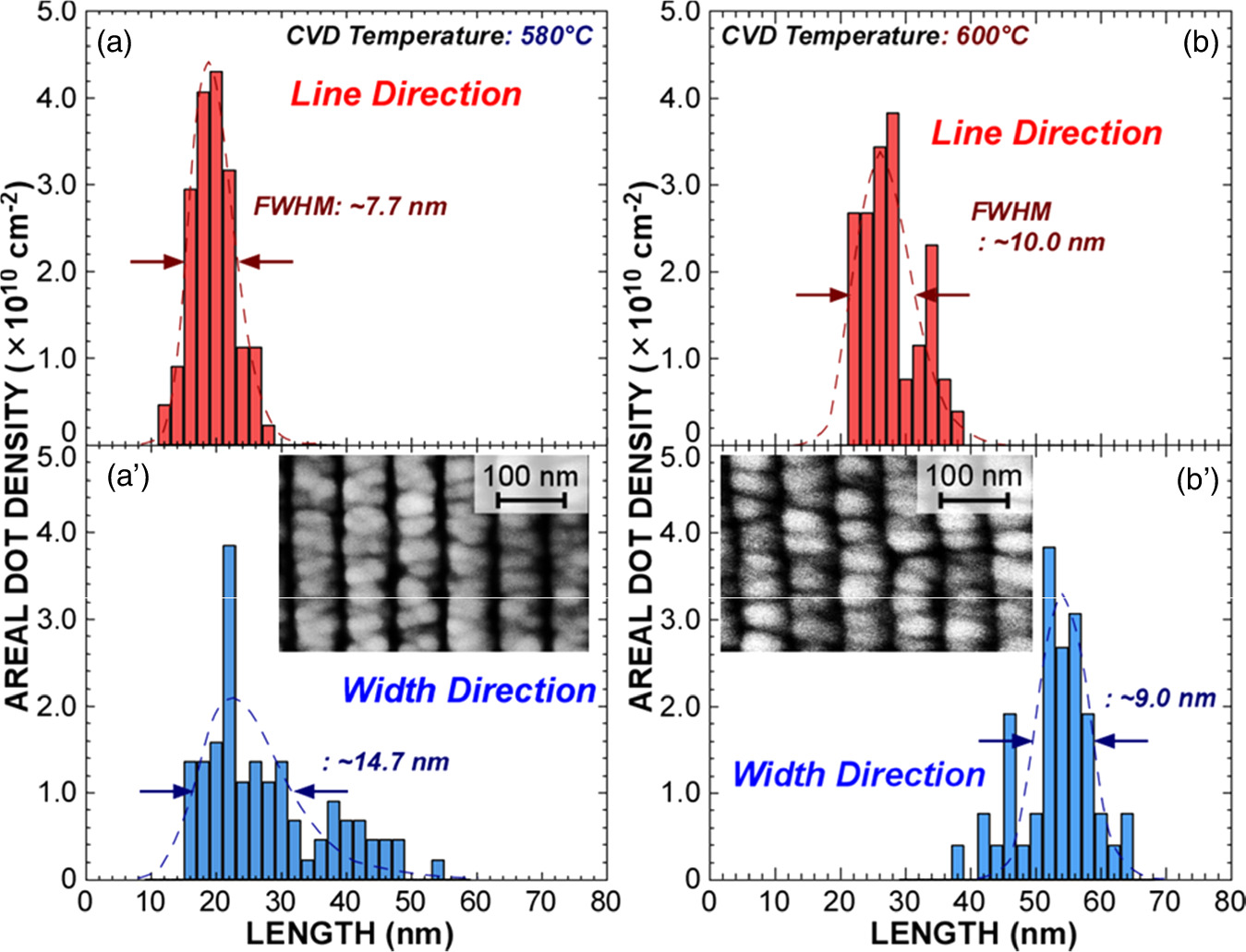
Fig. 7. Size distributions in [(a), and (b)] line, and [(a') and (b')] width direction of the Si-QDs formed on the 25 nm width SiO2 line patterns at [(a), and (a')] 580 and [(b), and (b')] 600 °C for 150 s evaluated from the SEM images. Typical SEM images of the Si-QDs on the 25 nm width SiO2 line patterns are also shown in the inset.
Download figure:
Standard image High-resolution image
4. Conclusions
We have fabricated Si-QDs on thermally grown SiO2 from 50 or 20 nm width line/50 nm space patterned and characterized the growth mechanism on the line patterns. Since the 50 nm width SiO2 line patterns are as long as the average surface migration length of Si precursors, the influence of precursors that migrated from the space regions was small. In the growth of Si-QDs in the line width direction on the 20 nm width SiO2 line patterns, the contribution of precursor from space regions could not be ignored, which results in elliptical growth. Finally, we have successfully demonstrated a one-dimensional arrangement of elliptical Si-QDs with high uniformity in size by controlling line width, CVD time, and temperature.
Acknowledgments
This work was supported in part by Grant in Aid for Scientific Research (A) 21H04559 of MEXT Japan, and Hibi Science Foundation.