
Abstract
The degradation of surface passivation performance by metallization is a challenge in realizing highly efficient crystalline Si solar cells that use novel carrier-selective contacts. Here, we report on a simple method to study the effect of metallization on passivation of titanium oxide (TiOx)/Si heterostructures. We investigated the relationship between the implied open-circuit voltage (iVOC) and the photoluminescence (PL) intensity imaging of solar cell precursors before metallization. Based on the relationship obtained, the change of the iVOC before and after metallization on the TiOx was evaluated quantitatively. The results showed that the iVOC predicted by the PL measurement decreases by 23–104 mV after metal deposition and shows a good agreement with the measured VOC in the finished solar cells. These results demonstrate that the iVOC evaluation by PL measurement provides a good prediction of the VOC after metallization, which is useful in analyzing the passivation degradation induced by metallization.
Export citation and abstract BibTeX RIS
1. Introduction
High-performance solar cells are essential, particularly for building- and vehicle-integrated photovoltaic applications. Silicon heterojunction (SHJ) solar cells using hydrogenated amorphous silicon (a-Si:H) as carrier-selective contacts (CSCs) have achieved a high power conversion efficiency (PCE) of >25%, which is enabled by the high passivation performance at the interface between crystalline Si (c-Si) and the intrinsic a-Si:H [a-Si:H(i)] layer, and by the excellent carrier selectivity of doped a-Si:H. 1–4) However, the energy loss still remains due to parasitic absorption in the short wavelength region caused by its low bandgap energy (Eg) of 1.7 eV. 5,6) In addition, the cost of a-Si:H film formation is still high, and therefore, it is necessary to design a new material that has a higher Eg and can be fabricated with a simple fabrication method for practical use.
To further improve the PCE of SHJ solar cells at a reduced cost, recent studies have focused on applying novel CSCs. CSCs are required to efficiently select and extract the carriers (electrons and holes) with high passivation performance. Replacing a-Si:H with a wider bandgap CSC material is attractive to reduce the parasitic absorption that was observed in the conventional SHJ solar cells. There are several candidates for CSCs: molybdenum oxide (MoOx ), 7–9) vanadium oxide (V2Ox ), 10,11) copper iodide (CuI), 12,13) nickel oxide (NiOx ), 14) magnesium oxide (MgOx ) 15–17) and titanium oxide (TiOx ). 18–27) Among them, TiOx has been intensively studied as an electron-selective contact (ESC) which selectively collects electrons. In principle, TiOx is much less prone to absorbing light than a-Si:H due to its wider Eg of 3.3 eV. Furthermore, TiOx /c-Si heterostructure can efficiently collect electrons due to its small conduction band offset (<0.05 eV) and large VB offset (>2.0 eV). 28,29) In addition, the atomic layer deposition (ALD) of TiOx has an advantage that the amorphous TiOx is uniformly deposited at the nanoscale and provides good passivation of the Si surface. Consequently, high PCE has been reported for solar cells using TiOx . 18,25,27) Note that TiOx can also work as a hole-selective contact by modifying the growth and the post annealing processes. 27) However, we focus on TiOx as an ESC in this work.
Although TiOx has these advantages, it has not yet been used in practical devices owing to some issues, for example, a high interface resistivity at the TiOx /metal contact 30) and degradation of passivation performance after metallization. 31) To solve the former issue, the attempts that use low-work function materials are made to introduce downward band bending. In fact, there are some reports to lower the contact resistivity by inserting low-work function materials such as LiF, 32) Ca, 33) and Mg. 34) On the other hand, the latter issue has not been addressed yet, and the degradation mechanism has not been fully understood. Therefore, mitigating the metallization-induced degradation is essential to use TiOx as an ESC in practical Si solar cells.
To understand the degradation mechanism, a quantitative evaluation of the passivation performance after metallization is essential. In general, implied open-circuit voltage (iVOC) is measured by the quasi-steady-state photoconductance (QSSPC) method and commonly used as an index of passivation performance. However, in principle, QSSPC is not applicable to metallized cell precursors because the conductance of metals is much higher than the photoconductance of Si wafers. Although open-circuit voltage (VOC) can be measured with finished solar cells, it is extremely time- and resource-consuming. Therefore, a quick and contact-less technique that enables to quantify the iVOC of metallized cell precursors is highly desired. Hallam et al. reported that iVOC correlates with photoluminescence (PL) intensity (IPL) if the samples have the same surface structure, and the IPL is converted into iVOC by using a calibration line. 35) This non-destructive and contact-less approach is applicable to solar cells even after metallization and suited to characterize the iVOC before and after metallization quickly.
In this study, we focused on the TiOx /Si heterostructures fabricated for ESC and evaluated the iVOC before and after metal deposition quantitatively by PL using a calibration line obtained from the relationship between pre-measured iVOC and IPL. Then, we tested the validity of the results by comparing the predicted iVOC based on PL with the VOC of the finished solar cells.
2. Experimental methods
All experiments were performed on double side mirror-polished, n-type c-Si(100) wafers. The resistivity and thickness were 1.0–5.0 Ω·cm and about 280 μm, respectively. An intrinsic and p-type a-Si:H (p/i) layer was deposited by plasma-enhanced CVD (PECVD) on the front side. The growth conditions of the p-type a-Si:H (p/i) layers were reported elsewhere. 36) After that, the substrates were immersed in a 5% HF solution to remove the native oxide layer on the rear side. Then TiOx was deposited on the rear side by thermal ALD (GEMStar-6, Arradiance Inc.). Tetrakis-dimethyl-amido-titanium (TDMAT), water vapor, and nitrogen (99.9999%) were used as a titanium precursor, oxidant, and purging gas, respectively. The TDMAT precursor bottle was heated at 60 °C during the ALD process. The titanium precursor supply line was maintained at 115 °C to avoid precursor condensation. The deposition temperature was 150 °C. The dose durations of TDMAT and H2O were 700 and 22 ms, respectively. The purge durations for TDMAT and H2O were 23 and 28 s, respectively. The TiOx thickness was varied in the range of 1–6 nm. After the TiOx deposition, hydrogen plasma treatment (HPT) was performed to improve the passivation performance. 37) There are many process parameters for HPT, including process temperature (THPT), process time (tHPT), H2 pressure (pH2), H2 flow rate (RH2), RF power (PRF), and electrode distance (d). In this study, these parameters were set at THPT = 373 K, tHPT = 90 s, pH2 = 100 Pa, RH2 = 70 sccm, PRF = 390 W, d = 10 mm based on our previous work. 37) After TiOx deposition, Mg and Al layers were subsequently deposited on the TiOx as electrodes by thermal evaporation. The Mg electrode was employed to reduce the contact resistance. 34) After each process, the iVOC and IPL (PL intensity per unit second) of the fabricated samples were measured by the QSSPC system (WCT-120TS, Sinton Instrument Inc.) and the PL imaging system (EPL-100s, Hamamatsu Photonics), respectively. After metal electrode deposition, only IPL was measured. A schematic of sample structures for iVOC and IPL measurements is shown in Figs. 1(a) and 1(b). In this study, the iVOC and IPL represent the averaged values over the 4 cm square in the center of the sample. The wavelength and intensity of the excitation light for the PL imaging were 940 nm and 100 mW cm−2, respectively. After the measurement of IPL, an indium tin oxide (ITO) layer and silver grid electrodes on the p-type a-Si:H [a-Si:H(p)] layer were deposited by sputtering with shadow masks to obtain the finished solar cells, followed by annealing at 160 °C for 2 h. The area of the substrates was 25 cm2, and the area of the finished solar cells defined by the front ITO layer was 1.12 cm2. A schematic structure of the fabricated solar cell is depicted in Fig. 1(c-1). The actual layout of the fabricated solar cell structure is shown in Fig. 1(c-2). Current–voltage (I–V) measurements were carried out under one Sun (air mass 1.5 global, 100 mW cm−2) illumination generated by a solar simulator to measure the VOC of solar cells. A shading mask was used to define the illumination area (1.045 cm2) slightly smaller than the cell area.

Fig. 1. Schematic sample structures for (a) iVOC and IPL measurements before metallization, (b) IPL measurements after metallization, (c-1) VOC measurements, and (c-2) a photograph of the solar cells (1.12 cm2) fabricated on a 5 cm x 5 cm c-Si substrate.
Download figure:
Standard image High-resolution image
Fig. 2. (a) Injection-dependent τeff for a p/i/c-Si/TiOx heterostructure with 1 nm thick TiOx . (b) iVOC before and after HPT as a function of TiOx thickness. The inset shows a schematic of measured samples.
Download figure:
Standard image High-resolution image3. Results and discussion
Figure 2 shows (a) the injection-level-dependent effective lifetime (τeff) and (b) the iVOC before and after HPT for various TiOx thicknesses. The iVOC values of an p/i/N/TiOx heterostructure before and after HPT with a 1 nm thick TiOx are shown in Fig. 2(a). Note that p, i, N represent a-Si:H(p), a-Si:H(i), and n-type c-Si wafer, respectively. It should be noted that the τeff of the samples is predominantly limited by the passivation performance of the TiOx side, which was confirmed by measuring the τeff of a symmetrically passivated sample (i.e. τeff ∼ 4 × 10⁻³ s was obtained in a p/i/N/i/p heterostructure at minority carrier density of 1 × 1015 cm−3). From Fig. 2(a), it was found that when the TiOx thickness was 1 nm, the sample showed a significant improvement in the passivation performance from an iVOC of 649 to 692 mV by HPT. This is possibly because the dangling bonds at the TiOx /c-Si interface were terminated by hydrogen. After HPT, however, the passivation performance was improved only for the sample with the TiOx thickness of 1 nm whereas it was degraded significantly for larger thicknesses, as shown in Fig. 2(b). In our previous work, we have reported that the best passivation performance was observed for the 1 nm thick TiOx /c-Si heterostructure after the HPT. 37) One possible cause of this degradation is due to the UV light soaking generated by HPT, 22) or the insufficient penetration of hydrogen radicals into the TiOx /Si interface when the TiOx film is thick. These results show that HPT under unsuitable conditions could cause considerable damage to the cell performance. However, the mechanism for the effect of HPT is still not well understood, and further investigations are necessary. Hereafter, we focus on our optimum TiOx /Si heterostructure with a 1 nm thick TiOx .
Figure 3 show the PL images of a p/i/N/TiOx heterostructure (a) before and (b) after the deposition of the Mg/Al electrode on the TiOx film (rear side). From the PL images, it is seen that the IPL is reduced from 1 × 10⁴ to 2 × 10³ counts s−1 by the rear metal electrode deposition. Here we note that the IPL of the metallized samples was corrected by subtracting the PL signal component arising from the reflection at the metallized rear surface (supporting information, Fig. S1). Figure 3(c) shows the relationship between iVOC and IPL for each sample before metallization. The iVOC and IPL of the p/i/N heterostructures without any passivation layer at the rear side were measured to be 570 mV and 200 counts s−1, respectively, which are considered as the lowest values of the poorly passivated sample. Thus, the samples showing iVOC < 570 mV and IPL < 200 counts s−1 were excluded from the linear regression to make an iVOC - IPL calibration line. From Fig. 3(c), a linear correlation was found between iVOC and the logarithm of IPL. The calibration line can be expressed as the following equation 35)

where C1 and C2 are constant prefactors, kB is the Boltzmann constant, and T is temperature. Here, the temperature was 295 K, which gives kB T = 25.4 mV. As shown in Fig. 3(c), the iVOC is well correlated with IPL with a coefficient of determination R2 of 0.88 in the range from 574 to 692 mV, which is in good agreement with the previous report. 35) The relatively large deviation seen for some samples is probably caused by the poor uniformity in the rear surface passivation, as the measured areas for the iVOC (∼3 cm2) by QSSPC and for the IPL (∼16 cm2) are different. Since the TiOx thickness is as thin as 1 nm in this study, the TiOx thickness nonuniformity even at a sub-nanometer scale is expected to cause a relatively large performance difference. Therefore, it is plausible that these anomalous values occur when the measurement areas of iVOC and IPL are not identical. Figures 3(d) and 3(e) show the iVOC,PL images before and after metallization, respectively, which were calculated using the IPL mapping and the calibration line. From iVOC,PL images, the areal distributions of iVOC,PL values can be visualized. The differences between the maximum and minimum iVOC,PL values are 29 mV before metallization and 54 mV after metallization, respectively. The tendency of the larger areal distribution of the iVOC,PL after metal electrode deposition was consistently observed in various samples, suggesting that the non-uniform metal formation on the TiOx layer influences the passivation performance.
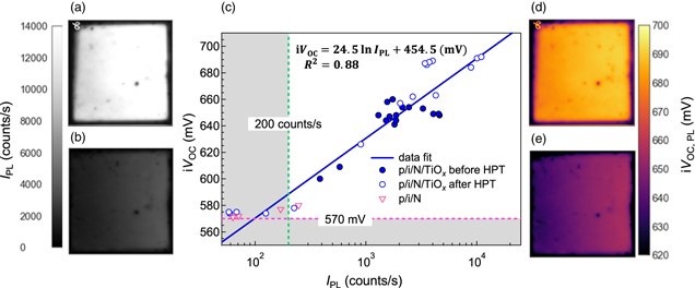
Fig. 3. PL images of the p/i/c-Si/TiOx heterostructure (a) before and (b) after metallization. (c) Correlation between the iVOC and IPL of the heterostructures before depositing metal on TiOx . The iVOC images calculated from the calibration line and IPL (d) before metallization, and (e) after metallization.
Download figure:
Standard image High-resolution imageFigure 4 shows the map of the saturation current density J0 (fA cm−2) (a) before HPT, (b) after HPT, and (c) after metallization. These maps were obtained using the following equation:

Here, iVOC,PL is used instead of VOC. q and JSC represent the elementary charge and the short-circuit current density, respectively. The JSC is assumed to be 32 mA cm−2 based on the actual values measured on the finished solar cells. As clearly seen in Fig. 4, we can confirm the decrease of J0 after HPT and the increase of J0 after metallization.
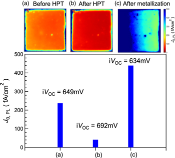
Fig. 4. Saturation current density J0 calculated from iVOC,PL (a) before HPT, (b) after HPT, and (c) after metallization. The images represent J0,PL mappings.
Download figure:
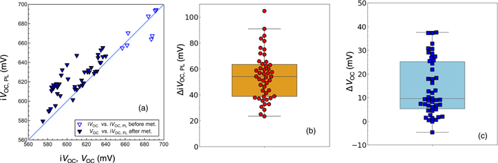
Standard image High-resolution imageThe actual VOC of solar cells was measured after the front electrode (ITO and Ag finger) deposition [see Fig. 1(b)]. Figure 5(a) shows the comparison between iVOC measured before metallization (open symbols) and VOC after metallization (closed symbols) of solar cells plotted against their corresponding iVOC,PL. The iVOC data in Fig. 5(a) represents only before metallization. The difference in the number of open and closed symbols is due to our experimental process, in which the VOC of several solar cells was measured from a substrate while the single iVOC was measured from a substrate. From Fig. 5(a), iVOC for the unmetallized sample and VOC for the metallized sample agree relatively well with iVOC,PL, respectively. A slight deviation of VOC from iVOC,PL will be discussed later. However, a substantial gap is found between iVoc before metallization and Voc after metallization in all samples. This gap indicates that passivation degradation by metal deposition occurs. Figure 5(b) shows the box and swarm plots of the iVOC,PL difference before and after metallization (ΔiVOC,PL). The ΔiVOC,PL is defined as the following equation,

Fig. 5. (a) Plots of iVOC and VOC versus iVOC,PL for the samples above IPL of 200 counts s−1 before and after metallization. (b) Box and swarm plots of ΔiVOC,PL and (c) ΔVOC.
Download figure:
Standard image High-resolution image
From Fig. 5(b), metallization-induced passivation degradation, which is represented as ΔiVOC,PL, was found in the range of 23–104 mV. Although the ΔiVOC,PL differs from batch to batch of the sample processes, the samples exhibiting high passivation performance result in a large ΔiVOC,PL as a general trend. This indicates that the passivation quality of the solar cells using the TiOx ESC is primarily limited by the metallization-induced passivation degradation.
From Fig. 5(a), it is found that VOC of all solar cells are lowered compared to the iVOC,PL. To discuss the reliability of the calibrated iVOC,PL with respect to the measured VOC of the solar cells, the gap between the iVOC,PL and the VOC of the finished solar cells (ΔVOC) is plotted in Fig. 5(c). The ΔVOC is expressed as

It is found that the ΔVOC values are within the range of −4 < ΔVOC < 38 mV. This gap is possibly caused by the VOC loss due to the imperfect carrier selectivity of both the TiOx electron contact and the a-Si:H(p) hole contact, as well as the process-induced damage caused by the sputtering of the ITO and Ag electrodes, and the following post-deposition annealing. Another possible cause is the perimeter effect 38) where the photogenerated carriers diffuse out from the cell edge toward the unilluminated region and thus carrier density in c-Si is decreased. This effect is more pronounced in the case of small area solar cells with high quality Si absorbing layers. Note that the cell area is defined in 1 cm2 using a shadow mask in this study. Further, high-quality Fz Si wafers were used as substrates. Hence, VOC were expected to be reduced to some extent owing to the perimeter effect.
Finally, we touch on the versatility of the method presented in this study. It is important to note that there exists an upper or lower performance limit for the PL imaging and QSSPC system if the passivation is too high or too low. In addition, since we have applied the method to our uncommon solar cell structures (i.e. a-Si:H(p)/a-Si:H(i)/c-Si/TiOx /Mg/Al), further study is necessary to conclude whether or not this method can be applied to various types of Si solar cells. In principle, this method is also applicable to c-Si cells with textured surfaces as well, though we used only polished Si wafers within this work. In that case, however, the optical effects caused by surface textures must be taken into account, particularly for the rear side metallization. Nevertheless, the above results suggest that the method presented here can provide a quantitative measure of the VOC loss caused by metallization and its post-fabrication processes of the solar cells that use novel CSCs.
4. Conclusions
The PL imaging technique was applied to quantitatively evaluate the iVOC of metalized c-Si solar cell precursors, which was not measurable by common photoconductance methods such as QSSPC. We applied this method to evaluate the surface passivation quality of TiOx -based CSCs in a-Si:H(p)/a-Si:H(i)/c-Si/TiOx heterostructures, which was often deteriorated by the metallization process. By measuring iVOC and IPL for the samples exhibiting different degrees of surface passivation, we obtained a linear correlation between iVOC and ln(IPL), which was used to obtain iVOC,PL. We confirmed a reduction in iVOC,PL of the Si heterostructures after the deposition of Mg/Al electrodes, indicating that the surface passivation at the TiOx -based CSC was deteriorated by the metallization. A good agreement was observed between the iVOC,PL and the VOC in the finished solar cells, suggesting that the PL imaging can be used to predict the VOC of the finished solar cells and to analyze its loss caused by the metallization process. Thus, this method would help in the fast development of Si solar cells using novel metal-oxide based CSCs.
Acknowledgments
This work was supported by the New Energy and Industrial Technology Development Organization (NEDO), JPNP20005 and MEXT, Grants-in-Aid for Scientific Research on Innovative Areas "Hydrogenomics," JP18H05514 and JP18H05518.
Supplementary data (0.1 MB PDF)