

Abstract
Investigations were made on the application of aqueous ethyltrimethylammonium hydroxide (ETMAH) as an alternative developer solution (compared to the de facto standard aqueous tetramethylammonium hydroxide or TMAH) for mainstream lithographic technologies; extreme ultraviolet (EUV), ArF immersion (ArFi), KrF, and i-line. Results show that for EUV, ETMAH at a specific developer concentration allows mitigation of resist-based stochastic defects while maintaining lithographic performance. It was also found that the ETMAH developer solution is compatible with the ArFi, KrF, and i-line lithography (ultimate resolution and line width roughness was maintained). For EUV, ArFi, and KrF lithography which utilizes chemical amplification resist (CAR) material platforms, sensitivity remained constant. For i-line lithography, sensitivity was observed to decrease by roughly 25%–30% when ETMAH was utilized, attributed to the different dissolution mechanism of the novolac-based resist compared to CAR. Nevertheless, these results show the viability of ETMAH as an alternative developer solution for mainstream semiconductor lithography.
Export citation and abstract BibTeX RIS
1. Introduction
Resist materials remain one of the main pillars in the realization of fine patterning for semiconductor manufacturing. 1–5) Stringent patterning requirements in next-generation semiconductor lithography have pushed for resist material technology to further advance to single-nanometer patterning capabilities. 6–9) However, these patterning targets are starting to challenge the physical limits of the polymers used in present mainstream resist materials (i.e. chemically amplified resist (CAR)). 3,5) Moreover, at these pattern sizes, new issues such as the occurrence or generation of resist-based random defects (also referred to as stochastic defects) need to be considered. 10–16)
The improvement and optimization of resist processes, which has not seen any significant changes for some time now, is one approach that may provide possible solutions to this issue. One specific example is the resist dissolution or development (after pattern exposure) that has remained the same in the last 30 years or so. At present, the resist development step has and continues to utilize the same type of developer solution; tetramethylammonium hydroxide (TMAH, MW = 91.15 g mol−1) at a fixed concentration of 0.26 N. 17,18) The industry's attachment to this de facto standard of 0.26 N TMAH has been reported to be more of an economical choice than optimal performance. 19–21)
With this as background, investigations on alternative aqueous alkali developer solutions have and are continuously being pursued. 22–27) In this paper, the authors focus on ethyltrimethylammonium hydroxide (ETMAH, MW = 105.18 g mol−1) as a potential alternative developer solution for semiconductor lithography.
2. Experimental procedures
2.1. Patterning experiments
A comparative investigation was made between the lithographic performance of resists developed in ETMAH utilized at various developer solution concentrations (from 0.33 to 0.10 N) and TMAH at the 0.26 N developer solution de facto standard concentration.
In these experiments, mainstream lithographic technologies such as extreme ultraviolet (EUV) (λ = 13.5 nm), ArF (λ = 193 nm) immersion or ArF immersion (ArFi), KrF (λ = 248 nm), and i-line (λ = 365 nm), matched with the respective optimal resist materials and their corresponding processes, were applied.
For EUV lithography, a widely-used EUV CAR material (that is generally a hybrid of polyhydroxystyrene (PHS) and methacryl polymers) 28) was utilized at a film thickness of 30 nm under optimal post-application bake (PAB)/post-exposure bake (PEB) conditions. The EUV CAR was coated on top of an organic underlayer at a thickness of 20 nm. Development and rinse processes (with de-ionized water) were utilized at 30 s and 20 s, respectively. For ArFi lithography, an ArFi CAR material (generally methacryl-based) 28) was utilized at a film thickness of 105 nm under optimal PAB/PEB conditions. The ArFi CAR was coated on top of a bottom anti-reflective coating (BARC) at a thickness of 95 nm. Development and rinse processes (with de-ionized water) were utilized at 30 s and 20 s, respectively. For KrF lithography, a KrF CAR material (generally PHS-based 29) was utilized at a film thickness of 435 nm under optimal PAB/PEB conditions. The KrF CAR was coated on top of a BARC at a thickness of 60 nm. Development and rinse processes (with de-ionized water) were utilized at 60 s (performed twice) and 20 s, respectively. Lastly, for i-line lithography, novolac-based resist material 30–36) was utilized at a film thickness of 1.1 μm under optimal PAB/PEB conditions. The wafer was primed with hexamethyldisilazane (HMDS) 37) before resist was coated. Development and rinse processes (with de-ionized water) were utilized at 60 s and 20 s, respectively.
EUV patterning exposures were performed using the NXE-3400 (ASML) with a 0.33 numerical aperture (NA). For ArFi, the NXT-1950Ai (ASML) with 1.35 NA was used. For KrF, the 0.73 NA FPA-5000ES3 (Canon) was utilized. And lastly, for i-line, patterning was done using the 0.57 NA FPA-5510iZs (Canon). Exposures were carried out using optimal illumination conditions.
Resist processes (coat, bake, etc.) were performed in in-line coater developer systems attached to each of the exposure tools. The development and rinse processes (with de-ionized water) were carried out using the SOKUDO DUO coater/developer (SCREEN Semiconductor Solutions). Pattern images and measurements were performed using the CG5000 scanning electron microscope or SEM (Hitachi High-Technologies).
2.2. Stochastic defect analysis for EUV lithography
For the EUV lithography experiments, stochastic defect analysis was carried out. Measurements were performed based on the 22, 18, and 16 nm 1:1 lines/spaces (l S–1) patterns. For these analyses, the ELX metric (stochastic defect margin), as previously reported, 22) was utilized. ELX is a modified formula of exposure latitude or EL, considering the presence of line-bridges in the underdose regions and line-collapse and/or line-breaks in the overdose regions [Eq. (1)]
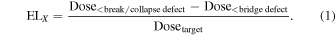
Dose<bridge defect means the lowest dose before bridge defects start to occur (underdose region) and Dose<break/collapse defect means the highest dose before line breaks and or line collapse start to occur (overdose region). Dosetarget indicates the dose at the target pattern size.
3. Results and discussions
3.1. EUV lithography application of ETMAH developer
3.1.1. Lithographic performance
Figure 1 indicates the EUV lithography patterning performance and stochastic defect margin ELX using the ETMAH versus TMAH developer solutions both at 0.26 N developer concentration. Results suggest no negative impact on resolution and line width roughness (LWR). A slight shift to higher sensitivity was observed for the ETMAH (37 mJ cm−2) compared to the TMAH developer solution (38 mJ cm−2). These results show the compatibility of the ETMAH as a developer solution for the EUV CAR resist.
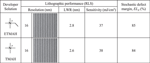
Fig. 1. EUV lithography patterning performance and stochastic defect margin ELX using the ETMAH versus TMAH developer solutions both at 0.26 N developer concentration.
Download figure:
Standard image High-resolution imageThe stochastic defect margin ELX of the 18 nm 1:1 l S−1 fabricated using the ETMAH developer solution was calculated to be 85% (compared to TMAH developer solution at 84%). These results indicate that at the 0.26 N developer concentration, comparable performance can be obtained for the ETMAH from the point of view of stochastic defect margin ELX . Next, further investigations were carried out to understand if 0.26 N is indeed the optimal concentration for ETMAH.
3.1.2. Developer concentration dependence
Figure 2 shows the effect of ETMAH developer concentration on lithographic performance metrics of (a) resolution, (b) LWR (based on at 18 nm 1:1 l S−1), and (c) sensitivity (based on at 18 nm 1:1 l S−1), and separately, (d) stochastic defect margin ELX . Results show that ultimate resolution (16 nm 1:1 l S−1) remains the same regardless of developer concentration [Fig. 2(a)]. LWR was also observed to be relatively smaller at developer solution concentrations between 0.26 and 0.15 N [Fig. 2(b)]. Sensitivity values meanwhile were found to increase at lower developer concentration [Fig. 2(c)].

Fig. 2. Effect of ETMAH developer concentration on lithographic performance metrics of (a) resolution, (b) LWR (based on at 18 nm 1:1 l S−1), and (c) sensitivity (based on at 18 nm 1:1 l S−1), and separately, (d) stochastic defect margin ELX .
Download figure:
Standard image High-resolution imageFigure 2(d) shows the dependence of stochastic defect margin ELX on ETMAH developer solution concentration. These results were calculated based on the SEM images obtained for the 22 nm, 18 nm, and 16 nm 1:1 l S−1 patterns at various exposure dose conditions. Results show that for the 18 nm and 16 nm 1:1 l S−1 patterns, an increase or improvement in stochastic defect margin ELX can be observed at developer concentrations around 0.20 N (compared to 0.26 N TMAH). However, for the 22 nm 1:1 l S−1 pattern, results show an improvement in stochastic defect margin ELX at higher developer concentrations.
3.1.3. Effect of low ETMAH developer concentration on EUV patterns
Results have shown that the ETMAH developer solution is compatible with the typical CAR material utilized in EUV. Even with the slightly larger molecular weight, the ETMAH developer produces equally effective patterning capability (lithographic performance and stochastic defect margin) as described in Sect. 3.1.1. Moreover, investigations on the effect of ETMAH developer concentration on patterning capability showed that LWR can be improved (while maintaining ultimate resolution) at developer concentrations lower than 0.26 N. Such lower developer concentrations are also advantageous as they have resulted in improved resist-based stochastic defect margins.
These improvements in LWR and stochastic defect margin obtained at 0.20 N ETMAH developer (compared to the standard 0.26 N) are assumed to be the effect of a change in the pattern formation process at this low developer concentration. Earlier papers on the visualization of the development process using in situ resist dissolution analysis (with a high-speed atomic force microscope) 38–40) have shown that during the development process at standard developer conditions (0.26 N TMAH), EUV pattern-exposed resist film undergo drastic physical changes such as nano-sized swelling before dissolving into the developer solution. 40) The use of lower developer concentrations minimizes the impact of these nano-sized resist swelling on the resist pattern formation process through the slow but smooth (subtle or moderate changes) dissolution of the exposed resist film. 40) Results shown in Fig. 2 indicate that this smooth pattern formation during dissolution in low concentration developer also improves stochastic defect margins.
It should be noted though that when the developer concentration becomes too low (or too high), the stochastic defect margin decreases. Results suggest that the optimal developer concentration is where sensitivity is maintained while the margin improvement is obtained. This is especially true for the 18 nm and 16 nm 1:1 l S−1 patterns but not for the 22 nm 1:1 l S−1 where a trend of increasing stochastic defect margin at increased developer concentration occurs. It is assumed that this may be the effect of patterning quality affected by photon shot noise 41–42) at the smaller pattern sizes (near the exposure tool's resolution limit).
3.2. Mainstream lithography (ArFi, KrF, i-line) application of ETMAH developer
3.2.1. ArFi lithography
Figure 3 indicates the ArF immersion lithography patterning performance using the ETMAH versus TMAH developer solutions both at 0.26 N developer concentration. Ultimate resolution was maintained at 43 nm 1:1 l S−1 in results obtained for both developer solutions. At this pattern size, LWR was observed to slightly improve with ETMAH at 5.3 nm (compared to 6.5 nm with TMAH). Optimal dose (sensitivity) was maintained for all patterns evaluated. These results suggest that ETMAH is comparable to TMAH in ArF immersion lithographic performance.
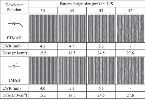
Fig. 3. ArFi lithography patterning performance using the ETMAH versus TMAH developer solutions both at 0.26 N developer concentration.
Download figure:
Standard image High-resolution image3.2.2. KrF lithography
Figure 4 indicates the KrF lithography patterning performance using the ETMAH versus TMAH developer solutions both at 0.26 N developer concentration. Ultimate resolution was maintained at 125 nm 1:1 l S−1 in results obtained for both developer solutions. LWR was observed to remain almost the same, and optimal dose (sensitivity) was maintained for all patterns evaluated. These results also suggest that ETMAH is comparable to TMAH in KrF lithographic performance.

Fig. 4. KrF lithography patterning performance using the ETMAH versus TMAH developer solutions both at 0.26 N developer concentration.
Download figure:
Standard image High-resolution image3.2.3. i-line lithography
Figure 5 indicates the i-line lithography patterning performance using the ETMAH versus TMAH developer solutions both at 0.26 N developer concentration. Ultimate resolution was maintained at 300 nm 1:1 l S−1 for both developer solutions, with resist residue in the pattern spaces as a limiting factor. LWR also remained almost the same for all the patterns evaluated. An obvious increase in patterning dose of around 100 mJ cm−2 (roughly 25%–30%) was observed when using ETMAH (compared to TMAH).

Fig. 5. i-line lithography patterning performance using the ETMAH versus TMAH developer solutions both at 0.26 N developer concentration.
Download figure:
Standard image High-resolution image
3.2.4. Effect of ETMAH developer on ArFi, KrF and i-line lithography
Results show that the ETMAH developer solution is compatible with other mainstream lithographic technologies such as ArFi, KrF and i-line lithography. This is especially true for ArFi and KrF lithography which utilizes CAR-type materials, where equally effective patterning capability was maintained even with the change of developers. Based on the results obtained at Sect. 3.1.2, improvements in LWR can be expected if the ETMAH developer concentration is optimized to lower values. Thus, further investigations on developer concentration dependence at these lithographic technologies are needed.
However, an obvious shift in optimal exposure dose (lower sensitivity) was observed for i-line lithography, even as ultimate resolution and LWR were maintained. As reported elsewhere, in the development process for novolac-based resist materials, two competitive reactions occur, compared to only one dominant mechanism for CAR. For novolac-based resist materials, dissolution is affected by (1) the complex formation between photoactive compound and novolac resin (inhibition effect) and (2) developer solution induced deprotonation of phenolic hydroxy groups in novolac resin (acceleration effect). 31) In contrast, the dominant dissolution mechanism for CAR-type materials is mainly due to the developer penetrating into the polymer film, which leads to the dissolution of deprotected polymer. 31,36)
The difference in optimal patterning dose due to developer change with the novolac-based resist is assumed to be due to its complex dissolution mechanism, which may be more sensitive to changes in developer molecular weight compared to the typical CAR. However, even with the sensitivity decrease, these results show the applicability of the ETMAH for i-line lithography.
4. Summary
These investigations show that in EUV, ETMAH at a specific developer concentration allows mitigation of resist-based stochastic defects while maintaining lithographic performance. Such improvements achieved at a lower developer concentration of 0.20 N (compared to the standard 0.26 N concentration) are assumed to be the effect of the minimized impact of nano-sized resist swelling on the resist pattern formation process through the slow but smooth (subtle or moderate changes) dissolution of the exposed resist film.
Results have also shown that the ETMAH developer solution is applicable and equally effective as the de facto standard TMAH for ArFi, KrF and i-line lithographic technologies. This is especially true for ArFi and KrF lithography which utilizes CAR-type materials, where equally effective patterning capability was maintained even with the change of developers. An obvious shift in optimal exposure dose (lower sensitivity) was observed for i-line lithography, even as ultimate resolution and LWR were maintained. The difference in optimal patterning dose due to developer change with the novolac-based resist was assumed to be due to its complex dissolution mechanism which may be more sensitive to changes in developer molecular weight compared to the typical CAR used in EUV, ArFi, and KrF lithography. However, even with the sensitivity decrease, these results show the applicability of the ETMAH for i-line lithography.
In summary, these investigations show the effectiveness and compatibility of the ETMAH developer solution for the application in the mainstream lithographic technologies of EUV, ArFi, KrF, and i-line.
Acknowledgments
We thank SACHEM, Inc. through the cooperation of NAGASE & Co., Ltd., for the ETMAH developer solutions used in these experiments.