

Abstract
Displacement Talbot lithography can rapidly pattern periodic nanostructures with high depth of focus over large area. Imperfections in the phase mask profile and the stage movement inaccuracies during the exposure cause linewidth variation in every second line of binary gratings. While this beating is barely visible in patterned photoresist, it leads to substantial depth variation when transferred into high aspect ratio silicon structures, because of micro-loading in deep reactive ion etching. A proper scan range compensated the defect, and a beating-free grating with pitch size of 1 μm and aspect ratio of 54:1 is demonstrated.
Export citation and abstract BibTeX RIS
Periodic micro- and nano-structures, such as gratings, pillar arrays, holes arrays, have been widely applied in many research fields. 1–7) Two critical requirements for such kinds of periodic structures are: (1) precisely controlled critical dimensions; (2) high local and overall uniformity. Silicon gratings with high aspect ratios are key optical components of grating-based X-ray interferometry (GI), 8,9) which has promising exploitation in medical diagnostic 10,11) and material analysis. 12) The recent development of this technology towards higher resolution and sensitivity demands gratings with smaller pitch size, higher aspect ratio and large area (in the order of 50 cm2 or higher), challenging the fabrication methods and boosting the related research in the fields of lithography, 13) etching 14–16) and metallization. 17–21)
Fabrication of silicon gratings includes two major steps. First, the grating pattern is prepared on the surface of a silicon wafer by lithography methods. Second, the pattern is transferred into the substrate through etching methods. 13–16,22) A phase shift grating could only require the silicon template, while for absorption gratings, the etched trenches have to be filled with highly X-ray absorbing materials, such as gold, 17,21,23,24) iridium, 18) tungsten, 25) etc. Since gratings are used in GI to detect subtle deflections in an interference pattern, any imperfections especially in the phase shift gratings, could affect the overall system's imaging performance. Therefore, gratings with high accuracy in pitch, duty cycle, height of the grating lines impressed in the substrate, and uniformity of these features over the entire patterned area are urgently required for grating-based X-ray imaging.
Displacement Talbot lithography (DTL) enables rapid patterning of periodic structures with feature sizes down to about 100 nm and improves the pattern uniformity on wafer scale. 26,27) DTL is a non-contact lithography method [Fig. 1(a)], and uses laser as light source. Like conventional UV lithography with mask aligners, DTL also needs a photomask to create the pattern, and the mask can either be of an amplitude or a phase type. The laser light passing through the periodic pattern of the photomask forms an interference pattern called Talbot carpet 28) [see Fig. 1(a)]. Commercial silicon wafers always have some bow, warp, total thickness variation and roughness imperfections, which result in nonuniformly exposed patterns, even if a high vacuum exposure mode is chosen for the mask aligner. This is no longer an issue for DTL, since the wafer is scanned contactless along the Talbot carpet for multiples of the Talbot distance (td ≅ 2p2/λ), 29) following a reciprocating movement along the laser propagating direction. The distance between the uppermost and downmost points of the movement defines the scanning range. The scanning movement theoretically guarantees that the unflattness of the wafer is compensated. However, in some of our exposure tests, an abnormal effect was still observed: two different alternating widths of trench in the developed photoresist reveal, as shown in Fig. 1(b), a sort of beating effect. The trench width difference is barely visible from the SEM images, but since the pitch is in the range between a few micrometers and sub micrometer, we expected the micro-loading effect (etching rate depends on feature size) 30) to play a relevant role, when deep reactive ion etching (DRIE), such as the Bosch process, is used for the following etching step. Consequently, the etching depth of adjacent trenches replicates the same beating phenomenon with a clear depth variation as shown in Fig. 1(c). This beating is considered to be a defect in grating fabrication and should be minimized to prevent the micro-loading effect from affecting the pattern transfer into the silicon substrate by DRIE.

Fig. 1. (a) Schematics of displacement Talbot lithography process: a phase mask with duty cycle 0.5 is exposed producing a Talbot carpet with half period, z defines the scanning direction perpendicular to the surface of the photomask, x defines the direction perpendicular to the lines; (b) beating defect in linewidth (a and b); (c) the grating lines (1 μm pitch) etched into the Si substrate by DRIE show the beating defect in depth of adjacent lines (ha and hb ) due to micro-loading.
Download figure:
Standard image High-resolution imageThe exposure process was simulated by introducing an offset in the mask's phase shift and a nonlinearity in the stage movement. First, the Talbot carpet was simulated with Fresnel approximation by fast Fourier transformation method, 31) since the wavelength λ of the light source, the pitch pmask and type (amplitude or phase) of the photomask are known. The used parameters were the following: λ = 377 nm, and π-phase shift photomask with pmask = 2 μm, which produces a pattern with pitch presist = 1 μm in the photoresist. The scanning range r is given by r = n × td , where td = 21 μm, and n is the number of td . For a given laser light intensity, the dose is determined by the exposure time t, which is also the total scanning time of the sample stage. The total exposure time t and the scanning range r are input data of the machine, which automatically adjusts the speed for the sample stage.
A uniform exposure can only be achieved under ideal conditions. Even in the case of error-free duty cycle, depth and profile shape, the edge effects due to the topography of the mask can affect the resulting exposure. 32) An in-house fabricated (nominal) π-phase shift photomask was used for the exposure test. The photomask was made of quartz, which has a refractive index of approximately 1.56 for a laser with a wavelength of 377 nm. 33) However, if the trenches in the photomask have not the right depth or have non-uniformities in the depth across the mask, the resulting phase shift deviates from π. Figure 2(a) shows how the Talbot carpet changes with increasing of the phase shift offset in the photomask. The depth of the etched grooves in the photomask was measured to be about 10% off the original design. This has a non-negligible effect on the produced pattern, as shown in Fig. 2(a). Therefore, we applied a compensated value of phase shift in the simulation in order to take into account the mismatched depth of the photomask. The phase shift for the simulation was then replaced by a reduced value corresponding to 90% of π, leading to an intensity fluctuation within the generated interference pattern. Further, another important factor with great impact on the resulting exposure is the moving trajectory of the sample stage. The sample stage is programmed to move the wafer up and down and to deliver a Gaussian dose distribution along the laser propagating direction. 34) Figure 2(b) shows the stage position as a function of time. In practice, the stage movement deviates from the designed speed function [blue dotted lines in Fig. 2(b)] during the exposure process, especially when the stage inverts the direction. The raw sample stage position during the exposure was acquired from the DTL system and plotted with the red solid line in Fig. 2(b). A scaling factor for the stage speed was then introduced in the simulation to imitate the real exposure time. Finally, the photon intensity map within the Talbot carpet was integrated over the scanning range to map the dose distribution in the photoresist. The scanning range was varied as multiples n of the td . Figure 2(c) shows the simulated dose distributions of the exposure processes for several scanning ranges (n = 1, 2, 4, 8), including the offset of phase shift and the imitated moving trajectory. The exposure threshold was set at half maximum intensity, in order to have a duty cycle of 0.5 in the patterned photoresist. For a short scanning range [see low n in Fig. 2(c)], the generated dose distribution is not uniform and shows a certain level of beating. The difference becomes less and less prominent as the scanning range increases [see high n in Fig. 2(c)]. The beating is smoothed out as the scanning range was increased up to 4 × td [n = 4 in Fig. 2(c)] and became barely visible as the scanning range went up to 8 × td [n = 8 in Fig. 2(c)]. Therefore, simply increasing the scanning range during exposure smoothed out the effect of phase shift deviation in the photomask.

Fig. 2. (Color online) (a) Talbot carpet produced by photomasks with different offsets in the profile height (photomask offset in the labels, 0% produces π shift); (b) position versus time of ideal sample stage (blue dotted line) and an example of real sample stage (red solid line); (c) dose distribution for different scanning ranges in multiples of Talbot distance, the x is defined in Fig. 1(a).
Download figure:
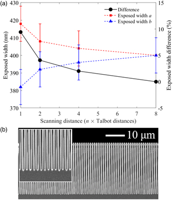
Standard image High-resolution imageThe experimental validation was performed on 4 inch 〈100〉 silicon wafers. The surface of the silicon wafer was coated with a Cr layer 100 nm thick, which served as the hard mask during the following DRIE step. SUMIRESIST PFI-88A7 positive photoresist was spun on top of a layer of AZ BARLi-II bottom anti-reflective coating. The DTL process was performed with an Eulitha Phable R200 tool using a pitch pmask = 2 μm linear grating as π-phase shift photomask, which produces a pitch presist = 1 μm linear grating pattern in the photoresist. A polarized laser source with a wavelength of 377 nm was chosen for the exposure, and the intensity of the laser light was set at 0.5 mW cm−2. An exposure time of 200 s was adopted for all the exposure tests. Different scanning ranges r (for n = 1, 2, 4, 8) were applied to different areas on the same wafer. The beating is visible in the SEM cross-section views of the photoresist at a magnification of 50 kX. An example corresponding to n = 1 is reported in Fig. 1(b), the line widths of adjacent lines are a = 418 nm and b = 382 nm (measurement accuracy of ±10 nm) respectively. Figure 3(a) reports the line width of adjacent lines in the photoresist as a function of the scanning distance in multiples of td .
Fig. 3. (Color online) (a) Linewidth (a and b) in photoresist as a function of the scanning distance (in units of Talbot distance); (b) cross-section SEM image of a beating-free 1 μm pitch high aspect ratio grating with optimized DTL process (scanning distance of 8 times the Talbot distance).
Download figure:
Standard image High-resolution image
The pattern was then transferred to the Cr hard mask by plasma etching, and the substrate etching was done by DRIE using the Bosch process in an Oxford Plasma100 system. The trench was etched with a low chamber pressure (15 mTorr) and high power (RF 50 W/ICP 800 W), the etching details were reported elsewhere. 14) The target etching depth was set above 25 μm and within the range of the available etching conditions. 14) Although the beating was not easy to notice without careful measurement after the lithography step, the etching results clearly revealed this issue since the micro-loading is quite effective for these feature size (trench width ∼500 nm) and aspect ratio (∼50:1). Cross-section SEM at a magnification of 5 kX was used to detect the difference in etching depth. An example of grating corresponding to n = 1 is reported in Fig. 1(c), the line depth of adjacent lines (a and b) is ha = 27.9 ± 0.5 μm and hb = 25.6 ± 0.5 μm, respectively. The difference in etching depth was quite severe for short scanning range, and it was smoothed out with increasing the scanning range. At a scanning distance of 4 × td , the depth of the etched trenches has a variation of 0.3 μm over a maximum depth of 25.1 μm, which is already enough to meet our target quality. 35) At a scanning distance of 8 × td , the difference between adjacent trenches was negligible and cannot be detected by SEM. An example of etching with an optimized scanning range (8 × td ) is reported in Fig. 3(b). A beating-free grating with a pitch presist = 1 μm and duty cycle 0.5 was etched into a depth of 27 μm, corresponding to an aspect ratio of 54:1.
In conclusion, the simulations explained how the beating effect was generated from the inconstant scanning speed during the DTL process and predicted that it can be partially compensated by increasing the scanning distance. Measuring the etching depth of DTL patterned gratings provided the experimental verification of the predictions. Increasing the scanning distance during the DTL process improved the duty cycle uniformity and reduced the micro-loading effect during the DRIE of high aspect ratio gratings. The scanning range of 8 times the td completely suppresses the beating for aspect ratio of 54:1.
Acknowledgments
The authors would like to thank the staff of Laboratory for Micro- and Nanotechnology at Paul Scherrer Institut for the facilities and Eulitha AG for continuous support. The authors acknowledge the support from: SNF R'Equip grant 206021_177036 "Displacement Talbot Lithography for micro and nanopatterning", SNF_R'Equip grant 206021_189662 "SiDRY", SNF Sinergia Grant CRSII5_18356 "Clinical GI-BCT", EU Grant ERC-2012-StG 31'0005 "PhaseX", SNF grant 159263, lottery fund SwissLOS of the Kanton of Aargau and Fondazione Gelu (TACI-C Project).