
Abstract
Bump-less copper (Cu) bonding is currently the most attractive approach for fine-pitch (<20 μm) 3D integration due to its compatibility with the wafer back-end-of-the-line (BEOL) fabrication process. In this study, themocompression bonding of bump-less Cu pads with a diameter of 4 μm and a pitch size of 10 μm was pursued, while chemical mechanical polishing (CMP)-processed Cu pads enclosed in SiO2 were employed with both protruded and recessed topographies. The effects of Cu topography (protruded or recessed) and bonding temperature on the electrical and microstructural properties of the die bonds as well as mechanical bonding strength were investigated. It was found that thermocompression bonding of CMP-processed Cu can be realized at shorter processing times, lower bonding temperatures, and pressures than standard electroplated Cu bonding. The bonding yield of the three configurations, i.e. protruded-protruded, protruded-recessed, and recessed-recessed Cu pads was also compared.
Export citation and abstract BibTeX RIS

This is an open access article distributed under the terms of the Creative Commons Attribution 4.0 License (CC BY, http://creativecommons.org/licenses/by/4.0/), which permits unrestricted reuse of the work in any medium, provided the original work is properly cited.
With the increasing demand for heterogeneous integration via 3D integration, there is significant interest in reducing interconnect pitch, since the smaller pitch enables simpler and more efficient circuits, resulting in reduced power consumption and design complexity. In terms of the interconnects' scaling roadmap, as solder micro-bumps and solder-capped Cu pillars hit their scaling limits, solder-free bump-less interconnects emerged as a viable option for 3D integration. Bump-less interconnect bonding permits higher pitch scaling, bump protection by dielectric or polymer, improved bump height uniformity, and yet a reduced total cost of ownership compared to conventional bumping. 1–3
Due to its compatibility with the wafer back-end-of-the-line (BEOL) fabrication process, bump-less copper (Cu) bonding is currently the most promising method for ultra-fine pitch (<20 μm) 3D integration. Cu bonding is an established wafer-to-wafer (W2W) bonding process at foundries. However, considering the increasing demand for heterogeneous chip stacking and high production yield with known good die (KGD), die-to-die (D2D), and die-to-wafer (D2W) Cu bonding processes still encounter technological challenges. 4,5 Cu bonding can be achieved through two means: either direct Cu bonding via thermal compression bonding (TCB) or two-step hybrid bonding. 6,7 While hybrid bonding is currently widely used in W2W bonding applications, its employment in D2D or D2W applications has been less widespread. This is due to the high sensitivity of hybrid bonding to particles, specially dicing debris, the processing and handling of surface-activated dies in die bonders, the sensitivity to the metal recess height, etc. 7–10 Hybrid bonding is often performed with recessed Cu surfaces (with a dishing height of 5 to 10 nm) surrounded by a dielectric layer (SiO2, SiN, and SiCN). However, the use of recessed Cu on one side and protruded Cu on the other side has recently gained attention. This is due to the generation of significant tensile stress after cooling in recessed-recessed bonds, which poses a reliability issue. The protruded-recessed bond can result in an optimal bondline form for hybrid bonding. 11 Beyne et al. also emphasized the advantage of a protruded-recessed Cu bond for down-scaling of hybrid bonding to sub-μm dimensions. 12 At sub-μm dimensions, the very limited Cu expansion can be an issue for conventional recessed-recessed hybrid bonding. To avoid high annealing temperatures, the reduced gap size of protruded-recessed Cu bonds would be favorable. 12
Direct Cu bonding has been primarily used for D2D and D2W bonding for Cu pillars. TCB of the electroplated Cu pillars requires high temperatures and high bonding pressures to compensate for pillar height deference. Cu does not melt or collapse upon bonding; therefore, a high bonding temperature is required to soften and increase the surface self-diffusion of Cu. Height variations of more than one micrometer are typical in plated Cu pillars. 4,13 Also, applying high pressures (>250 MPa) and lengthy processes (>15 min) is not suited to high-volume production. 4
In our previous studies, two approaches for enhancing the TCB of Cu pillars were proposed. The first approach was to exploit ultrasonic energy and induce mechanical vibrations, which promote interfacial atomic diffusion. Thermosonic Cu bonding was facilitated by lower bonding forces and a shorter process. 14 The second approach was to implement a planarization process (fly-cutting) on Cu pillars prior to bonding. As a result, Cu pillars with a flattened surface and a uniform thickness distribution through the wafer were generated. The proposed planarization process led to an increase of up to 60% in the contact area. 15 Nonetheless, these studies were conducted on Cu pillars with a diameter of 100 μm and a large pitch size of 350 μm which are not categorized in the ultra-fine pitch class. In another study by Bajwa et al., ultrafine pitch (10 μm) bonding of Cu pads was carried out. 16 The Cu pads were fabricated via the damascene process with a 1 μm protrusion and capped with a very thin layer of Ni-Au to avoid oxidation upon bonding at 350 °C. 16
In this study, ultrafine-pitch direct bonding of Cu pads embedded in the SiO2 layer will be investigated, while the bonding performance of both topographies of Cu pads after chemical mechanical polishing (CMP), i.e., recessed and protruded Cu 17 will be assessed. So far, direct TCB bonding has been performed only on protruded Cu surfaces. The purpose of this investigation is to look into the possibility of direct bonding between recessed-protruded and recessed-recessed pairs.
Experimental
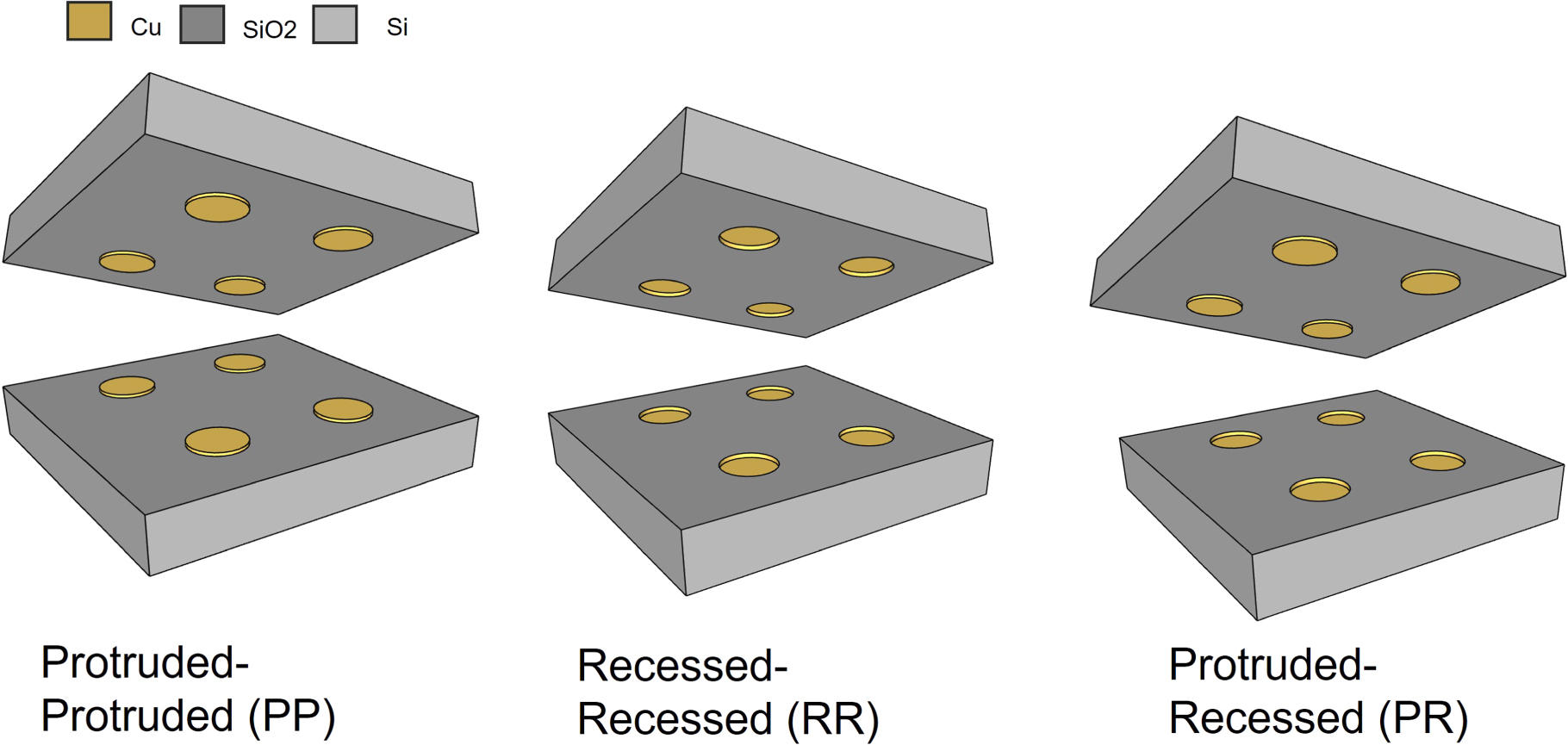
300 mm silicon wafers with an ultra-fine pitch (Cu/SiO2) daisy chain structure (i.e., Cu pad diameter of 4 μm and pitch size of 10 μm) were used for this study. The area fraction of Cu at the surface of the chips was 12,5%. Different CMP processes were applied to the wafers to achieve wafers with Cu recession and protrusion. 4 Cu protruded wafers and 4 Cu recessed wafers were fabricated. In previous studies, 12,18 the fabrication of Cu surfaces with recessed or protruded topographies using different CMP processing parameters (e.g., Cu/barrier polishing slurries, pads, polishing pressure, and time as well as the polishing rate selectivity) was described. The Cu protruded wafers with an average height of +13 nm are denoted as "P", whereas the Cu recessed wafers with two recessed heights of −9 and −5 nm are denoted as "R". For dicing the wafers, the stealth dicing singulation method was performed since it yields lower particle contamination compared to blade dicing. Here, a protective resist was spin-coated on the surface of the wafer during the dicing process to secure a particle-free Cu surface and minimize the contamination level. This layer was removed prior to bonding. As depicted in Fig. 1, the aim of this study is to evaluate the direct bonding of the recessed and protruded dies in three configurations, i.e., PP, PR, and RR. Each die consists of a matrix of 79 daisy chains with 2922 Cu bumps enclosed in SiO2. The pattern on the top die forms half of a daisy chain structure. The other half of the daisy chain structure is on the mating bottom die surface. The top die has a size of 9,5 × 10 mm, whereas the bottom die has a size of 10 × 10 mm. The contact pads on both edges of the bottom wafer were used for electrical measurements. The atomic force microscopy (AFM) measurements are presented in Fig. 2, manifesting a root mean square roughness (Rq) of 0.42 nm and 1.07 nm for SiO2 and Cu regions, respectively.

Figure 1. Three direct bonding configurations with respect to Cu/SiO2 surface topographies; Die bonding with two protruded Cu dies (PP), two recessed Cu dies (RR), and protruded Cu dies bonded to recessed counterparts (PR).
Download figure:
Standard image High-resolution image
Figure 2. Surface roughness analysis of the Cu pads and the surrounding SiO2 regions.
Download figure:
Standard image High-resolution imageFor D2D bonding, a die bonder with sub-micron placement accuracy (Finetech, Germany) was used. The bonding was conducted under an N2 atmosphere at 400 N and different bonding temperatures from 200 °C to 400 °C. The D2D bonding process began with the pick and placement of the bottom die, followed by the top die being picked by the tool and aligned to the bottom die using the chip's alignment marks. The top die was then brought into contact with the bottom die. The bonding area was then purged with N2 gas and heated to the specified temperature. The bonding duration was set to 3 min while a 400 N force was applied to the stack. Finally, the bonded dies were cooled down to room temperature. The bonder alignment was optimized to achieve <1 μm alignment accuracy at high temperatures in order to bond the die with 10 μm circular Cu pads.
Scanning electron microscopy (SEM) and electron backscatter diffraction (EBSD) characterization were carried out using a ThermoFisher Quanta 250 FEG system equipped with an EDAX Hikari Super EBSD camera. EBSD measurements on cross sections of the Cu interconnects were performed under low vacuum conditions (0.3 mbar, water vapor) with a 20 kV acceleration voltage and a 7.2 nA electron beam current. EBSD data for the Cu interconnects was recorded using EDAX TEAM 4.6 software, perpendicular to the bonding interface. Twenty Cu interconnects per sample were investigated. The analysis of the EBSD data was performed using the OIM Analysis 8.0 software package. The directional designations used for the EBSD mappings in this study are A1 [100] for the direction normal to the bonding interface, A2 [010] parallel to the bonding interface, and A3 [001] normal to the cross-section. For reliability analysis, isothermal storage at 400 °C under vacuum for 20 h was performed.
Moreover, a finite element method (FEM) using ANSYS 21.2 was also used to simulate the behavior of the Cu/SiO2 surface upon heating and bonding. All materials in the study are considered linear isotropic. Temperature variations in Young's modulus of Cu as well as the coefficients of thermal expansion of SiO2, Cu, Si, and Ti are taken into consideration. The nonlinear stress-strain relationship of the Cu was implemented in the simulation by using the Ramberg-Osgood model. 19,20 The bond shear strength of the samples was also evaluated by using a shear tester (Optima 4000 plus, Nordson Dage) at a speed of 30 μm s−1 at room temperature.
Results and Discussion
D2D pick & placement
Figure 3 shows the cross-sectional and bird's-eye views of the D2D-bonded chips. The placement precision of the die bonder plays a crucial role in direct Cu bonding since even a small misalignment can result in an electrical yield loss in ultra-fine pitch bonding. By using a sub-micron precision die bonder, utilizing chips with explicit alignment marks, and optimizing the alignment process flow for high temperatures, a superior placement accuracy of 1 μm was achieved. This alignment precision was adequate for the pad size of 4 μm and pitch of 10 μm. It is noteworthy to mention, that both heating-aligning approaches (i.e., room temperature chip alignment followed by heating and alignment of the already heated chips) rendered precise placement and similar results.

Figure 3. The cross-sectional (a) and bird's-eye view (b) of the D2D bonded chips.
Download figure:
Standard image High-resolution imageElectrical characterization
Figure 4 presents the cumulative percentage resistance of the direct bonded samples of different configurations (PP, PR, and RR) at different temperatures. It can be seen that the best performance in terms of yield and electrical conductivity was achieved in PP samples, especially at temperatures above 300 °C. The PR samples also rendered bonds with high yield, but with slightly higher contact resistance compared to PP samples and at a higher temperature (≥350 °C). Interestingly, RR samples also revealed electrical continuity, but at substantially lower yields and contact resistances. As inferred from this figure, direct Cu bonding of CMP-processed samples can be done even with a short bonding time (3 min) and a low pressure of 32 MPa. If we assume that the processing temperature, pressure, and time comprise the iron triangle of Cu bonding, it is evident that CMP-processed Cu pads offer advantages on all sides of the triangle, i.e., shorter bonding times, lower bonding temperatures, and lower bonding pressures than non-CMP processes Cu bumps. It is worth noting that, similar to our previous investigation for Cu pillars, 14 ultrasonic-assisted TC bonding, also known as thermosonic bonding, was attempted. However, the accurate placement of the ultra-fine-pitch dies was hampered by mechanical vibrations induced during thermosonic bonding. As a result, all of the daisy chains rendered an open circuit, and thermosonic bonding was determined to be incompatible with ≤10 μm pitch Cu bonding. The bonding yield of high-temperature PP and PR bonds was around 80%–90%. The reason for not reaching higher values was attributed to the high-temperature processing, which causes rapid Cu oxidation. In another study, a yield of 92% was reported for D2W hybrid bonding. 4

Figure 4. Cumulative percentage resistance of the direct-bonded samples of different configurations (PP, PR, and RR) at different temperatures.
Download figure:
Standard image High-resolution imageMicrostructural analysis
The microstructural evolution of the bonding interface was assessed by cross-sectional SEM and EBSD analysis. In this chapter, the Cu/Cu interface will be discussed, and in the following chapters, the SiO2/SiO2 interface will be addressed. Figures 5a and 5b show the cross-sectional images of the PP-bonded samples at 400 °C and 250 °C, respectively. At 250 °C, the Cu–Cu bondline is discernible, as highlighted with the black arrow in Fig. 5b. Cu/Cu atomic bonds are rather weak at low temperatures due to the limited plastic deformation of Cu at the interface and the slow solid-state diffusion of Cu. Typically, TCB can even be fostered at these low temperatures by increasing the external pressure or time which is undesirable for many applications. In some cases, higher pressure is permissible, but in our scenario, the pressure was maintained at 400 N (or 32 MPa), the highest force that the die-bonders could provide. It is noteworthy to mention that, similar to this study, low-pressure and low-temperature TCB was reported for CMP-ed Cu surfaces before. 21–23 In fact, the surface roughness of Cu plays a significant role in TCB, especially in the initial step of the bond. In TCB, Cu–Cu bonds are formed through the diffusion of atoms via grain boundary self-diffusion and interface diffusion. Surface roughness hampers interface diffusion as the asperities between the two surfaces act as a diffusion barrier layer, reducing atomic contacts. 24 As a result, TCB of CMP-ed Cu can be realized at lower bonding parameters than electroplated Cu bumps. 21 Typical bonding temperatures for non-CMP-ed Cu pillars are 380 °C–450 °C at pressures in the range of 30–120 MPa and for more than 30 min. 25

Figure 5. The cross-sectional SEM images (a)–(c), EBSD inverse pole figures (d)–(f), and grain boundary distribution (g)–(i) of the bonded samples at three different configurations: PP @ 400 °C (a), (d), (g), PP @ 250 °C (b), (e), (h), and PR @ 400 °C (c), (f), (i).
Download figure:
Standard image High-resolution imageSince the yield strength of Cu decreases with increasing temperature, the pressure demand for TCB can be reduced significantly at higher temperatures. The decrease in yield strength with increasing temperature is attributed to the thermal activation of dislocation motion, which boosts plastic deformation. 26 With a sufficient pressure and temperature combination, the material initially breaks through the brittle native oxide and deforms plastically at the bonding interface, filling the asperities and bringing the two surfaces closer to the interatomic distance. As inferred from Fig. 5a, the Cu/Cu bondline is not discernable at 400 °C, indicating successful bonding. The cross-sectional image of the PR bonded sample at 400 °C (Fig. 5c) also implies an invisible bondline at the Cu/Cu interface, manifesting the effect of temperature.
The grain structure of the bonded samples is also depicted in the inverse pole Figs. 5d–5f and the corresponding grain boundary distribution (IQ map) is found in Figs. 5g–5i. It can be inferred from Figs. 5d, 5g that the bonded interface turned into a high-angle grain boundary (HAGB), and upon accelerated intergrowth of Cu grains at 400 °C, a nonplanar interface resulted. On the contrary, Fig. 5e, 5h present a planner high-angle boundary at the interface, indicating a slow intergrowth between the two surfaces. It has previously been reported that the higher the nonplanarities, the greater the intergrowth and bond strength. 27–29 Figures 5f, 5i show a non-planar interface for the PR sample, confirming its good electrical performance. In Figs. 5g–5i, low angle (2 °C–5 °C), high angle (55 °C to 65 °C), Σ3 and Σ9 twin boundaries are drawn, where Σ3 boundaries were the most dominant boundaries in all the samples. Similar observations for hybrid bonded samples were reported before. 27,29
Bond strength analysis
The ultimate shear strength (USS) of the samples is plotted in Fig. 6a. An increasing trend in bonding strength with temperature is evident here. Also, it can be seen that the PP-bonded samples exhibit a slightly higher bonding strength compared to the respective PR samples. According to the military standard (MIL-STD 883E), a minimum shear strength of 6.08 MPa is required for die-bonding. 30 As inferred from this plot, high-temperature bonded PP and PR samples could fulfill the requirements, whereas the RR direct-bonded samples yield an inferior bonding strength. The shear test results were in good agreement with the electrical daisy chain results (Fig. 4), manifesting the robust Cu–Cu bonding in PP and PR samples at a temperature of ≥300 °C. Figure 6b shows an example of the fracture surface of the high-temperature bonded PR samples, implying a cohesive failure mode. All the samples were fractured at the bonding interface.
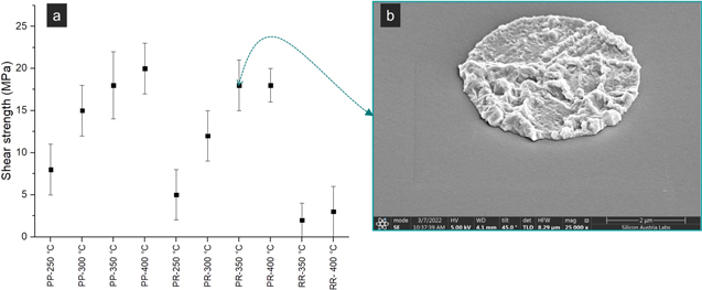
Figure 6. Ultimate shear strength of the direct bonded samples (a) and an example of a sheared Cu pad (PR-350 °C) implying a cohesive failure mode (b).
Download figure:
Standard image High-resolution imageCu pumping
In the previous chapters, it was observed that not only PP-bonded samples were electrically bonded, but also PR and RR samples. Furthermore, the shear analysis revealed that all of the samples had viable Cu-Cu bonding, albeit with different bonding strengths. Concerning PP pairs, it is evident that the Cu surfaces come into intimate contact even at room temperature. However, for recessed samples (PR and RR), the amount of Cu thermal dilatation (or pumping) required to reach the other surface and form a metallic bond is critical. While PR samples may have room temperature Cu contact, the RR bonding process exclusively relies on Cu expansion due to differential CTE between Cu and the surrounding oxide to bridge the room-temperature recess gap and concurrent Cu–Cu inter-diffusion.
In order to understand the amount of Cu pumping, FEM simulations were conducted. The results are shown in Fig. 7. It was found that Cu in protruded (P) samples extends to 64.5 nm at 400 °C and retains 30 nm above the SiO2 level after cooling. Similarly, in recessed (R) samples, the Cu pumping reaches 42.3 nm at 400 °C and remains 8.6 nm above the surface after cooling to ambient temperature. The amount of Cu pumping was also experimentally verified using high-temperature AFM tests (not shown here). The result revealed that even within the short bonding process window, the Cu pumping was executed completely, implying that the Cu pumping is not a lengthy process per se. Consequently, it can be assumed that, thanks to the Cu pumping, there was always metallic contact for both recessed and protruded Cu samples at the bonding temperature. The bondability of RP and RR samples at high temperatures can be explained by this effect. According to the simulation results, the minimum temperature for metal-metal contact in RR samples is 320 °C. This is consistent with the electrical and shear-test analyses, in which samples above this temperature (RR-350 °C and 400 °C) demonstrated electrical continuity and possessed superior bond strength.

Figure 7. FEM simulation results of Cu pumping for protruded and recessed samples; (a), (d) show the model geometries. (b), (c) present the initial topography of the protruded and recessed samples. The Cu pumping amount at 400 °C is illustrated in (e), (f), and those after cooling to room temperature are depicted in (h) and (i). In (g), the Cu pumping flow during heating and subsequent cooling is plotted.
Download figure:
Standard image High-resolution imageThus, it can be deduced that direct Cu bonding with different surface topographies, i.e., (PP, RP, and RR), is achievable. However, the poor electrical yield and the low shear strength of the RR samples suggest that a weak bonding interface was formed in those samples. The fractured surface of the RR samples after shear testing also showed a brittle fracture mode at the interface. This can be attributed to the formation of weak cohesive forces at the interface of RR samples. These cohesive bonding forces keep the two surfaces of RR samples bonded together during cooling and compete with the contraction forces, which tend to pull the two surfaces apart. 31 It can be postulated that the bonded interface in RR samples, which had only a few nanometers of protruded Cu at each side, was not strong enough to withstand the shrinkage of Cu upon cooling.
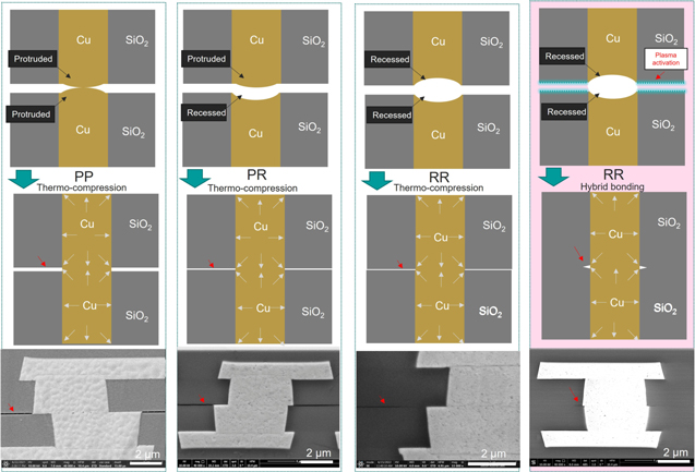
Gap size analysis in the SiO2 interface
The gap in the unbonded (SiO2/SiO2) interface is another observation in the direct bonding of Cu pads surrounded by SiO2. Figure 8 depicts various direct bonding procedures as well as the corresponding gap at the SiO2 interface. As a comparison, RR samples were hybrid bonded using N2 plasma-activated SiO2 bonding and annealing at 350 °C. There is a clear distinction between direct and hybrid-bonded samples in terms of SiO2 gaps, with the hybrid-bonded samples also receiving support from SiO2-SiO2 covalent bonds. Nonetheless, there appears to be a side crack in the SiO2 region as a result of the increased thermal stress and CTE mismatch. SiO2 cracking in hybrid-bonded materials has been reported frequently, particularly when the amount of Cu dishing is insufficient. 27 SiO2 is not expected to be bonded in direct-bonded samples. However, it can be seen that using PR and RR samples reduces the gap size in the SiO2 region. According to the FEM simulations and cross-sectional analysis, the maximum gap sizes in the PP, PR and RR samples were 59.6, 38.0, and 16.1 nm, respectively. It is worthwhile to mention that for the direct-bonded samples, an underfilling agent can be added subsequently to improve the samples' reliability.
Figure 8. Schematic illustration of the bonding mechanisms for PP, PR, and RR samples and the corresponding SEM images. The gap at the SiO2 interface is highlighted with a red arrow.
Download figure:
Standard image High-resolution image
Reliability analysis
The daisy chain resistance of bonded RR, RP, and PP samples was compared after they were kept at 400 °C for 20 h. A small resistance decline of about 1%–3% was noticed. Aside from that, no major changes in sample functionality were found, i.e., none of the working samples failed or showed an open circuit, and none of the non-functional samples became functional. Conclusively, the results indicate that direct-bonded Cu bonds are highly stable and reliable, capable of withstanding high temperatures in post-processing operations or service conditions.
Conclusions
In this study, D2D ultra-fine-pitch thermocompression bonding of bump-less Cu pads enclosed in a SiO2 layer after CMP processing was pursued. It was shown that both protruded (P) and recessed (R) Cu topographies can be bonded together in different configurations, namely PP, PR, and RR. While high-temperature PP and PR samples showed a high yield of (80%–90%), the RR samples rendered a lower yield of (20%–30%). Shear test results indicate that the bond strength of the PP and PR samples can reach up to 20 and 18 MPa, respectively, while a bond strength in the range of 4 MPa was obtained for RR samples. It was suggested that due to lower surface roughness and height variation, CMP-processed Cu surfaces allow shorter thermocompression bonding time and require lower external forces. It was implied from this study, that direct (thermocompression) bonding can be used as an alternative to hybrid bonding for Cu/SiO2 samples, especially where surface activation faces difficulties to be practiced (e.g. high surface roughness, improper dishing height or PP and PR formats, lack of plasma equipment, etc.) It was also found that the gap at the SiO2 surface can be reduced by using RR and RP pairs. Conclusively, it was verified that robust, thermocompression bonding of CMP-processed Cu pads with a diameter of 4 μm and pitch size of 10 μm can be performed by using a high-precision die bonder at a low bonding pressure of 32 MPa, and a temperature of ≥300 °C in only 3 min. It was found that Cu pumping enables thermocompression bonding of recessed samples at temperatures above 320 °C.
Acknowledgments
This work has been supported by Silicon Austria Labs (SAL), owned by the Republic of Austria, the Styrian Business Promotion Agency (SFG), the federal state of Carinthia, the Upper Austrian Research (UAR), and the Austrian Association for the Electric and Electronics Industry (FEEI).
Statements and Declarations
Data will be made available on request. This article does not contain any studies involving human or animal participants. All authors consent to the publication of this paper.