
Abstract
A SiCNO film containing 28% nitrogen was formed by plasma-enhanced chemical vapor deposition with no heating assistance using SiH3CH3, N2 and Ar gases. The 15 nm thick layer of the film was then etched off utilizing 10% ClF3 gas at room temperature for 1 min. After etching, the fluorine and chlorine concentrations within the film did not increase but they became higher at the surface. The removal rate of Si–N component was considered to be faster than that of Si–C, Si–O and C–N components, based on the X-ray photoelectron spectroscopy results. Overall, the etching was considered to occur following the etching behavior of the components formed between four elements, that is, Si, C, N, and O.
Export citation and abstract BibTeX RIS

This is an open access article distributed under the terms of the Creative Commons Attribution 4.0 License (CC BY, http://creativecommons.org/licenses/by/4.0/), which permits unrestricted reuse of the work in any medium, provided the original work is properly cited.
Various chemical conditions, 1 such as a corrosive environment at high temperatures and high humidity, are frequently and necessarily applied to advanced tools and devices. For such conditions, the tools and devices need to have a protective function. One of the effective ways is an anticorrosive coating which can be produced by thin films made of SiC, SiN, SiO2, SiON, SiCNO, etc. 1–5
Because a SiCNO material is expected to have properties consisting of the mixed advantages of SiC, SiN and SiO2, the SiCNO film was produced by a plasma-enhanced chemical vapor deposition (PECVD). 6–10 In a previous study 10 for evaluating the anticorrosive nature of the SiCNO film, a significantly strong etchant, such as ClF3 gas at 100% and at atmospheric pressure, was used. The etching was shown to be significant at high temperatures. Additionally, the film containing the nitrogen atoms at high concentrations was found to be easily etched off at room temperature. For applying the SiCNO film for various applications, the details of the etching behavior should be clarified, particularly, about the influence and role of nitrogen contained in the film and the overall surface condition after the etching.
In this study, the PECVD technique with no heating assistance was utilized for designing and preparing the SiCNO film. 10–13 The formed film was exposed to the 10% ClF3 gas, which was strong but milder than that used in the previous study. 10 The surface chemical conditions and the contents in the film were analyzed in detail to study the process during the etching.
Experimental
This study used the parallel plate PECVD reactor having 80-mm-diameter upper and lower electrodes for the glow discharge (Soft Plasma Etcher-SE, Meiwafosis Co., Ltd., Tokyo, Japan.), 10–14 as shown in Fig. 1. The acrylic resin chamber between the electrodes was 62 mm high. There were fluorocarbon resin rings attached along the two electrodes.

Figure 1. PECVD reactor and process in this study. Step (A) is the surface cleaning by Ar plasma and Step (B) is the SiCNO film deposition utilizing SiH3CH3, N2 and Ar gases.
Download figure:
Standard image High-resolution imageThe substrate was an aluminum plate (10 mm wide × 10 mm long). At Step (A) shown in Fig. 1, in order to remove the native oxide and contaminants 15 prior to the film deposition, the aluminum substrates were exposed to Ar plasma for one minute at 6 Pa and room temperature.
During Step (B), the SiH3CH3, N2 and Ar gases (99.9999% without further purification) were added at 6, 39 and 55%, respectively, at the pressure of 18 Pa for five minutes without any heating and at the average electric current of 9.8 mA. The oxygen was assumed to be incorporated into the film from the trace amount of remaining gases, such as O2, H2O, CO2 and CO. The Si, C, N and O concentrations have been reported to have a relationship with the electric current and the SiH3CH3, N2 and Ar partial pressures. 14
Next, the obtained SiCNO film was placed in the reactor, as shown in Fig. 2a, for the etching. The SiCNO film was exposed to the 10% ClF3 gas in the ambient nitrogen at atmospheric pressure and room temperature for one minute. The total gas flow rate was 1 slm. An aluminum surface was immediately covered with an aluminum fluoride thin film 16 which could prevent the back side of the aluminum substrate from etching by the ClF3 gas. After terminating the ClF3 gas, the sample was kept in the ambient nitrogen at 1slm for ten minutes, then the sample was removed from the etching reactor.

Figure 2. (a) Reactor and (b) process for exposure to ClF3 gas.
Download figure:
Standard image High-resolution imageThe chemical bonding conditions of the film surface were ex situ evaluated by X-ray photoelectron spectroscopy (XPS) (Quantera SXM, ULVAC-PHI Corp., Tokyo, Japan). The depth profiles of the Si, C, N, O, F and Cl in the film were obtained by secondary-ion mass spectrometry (SIMS) (PHI ADEPT1010, ULVAC-PHI Corp., Tokyo, Japan). The C, N, F and Cl concentrations were calculated from their secondary ion strength using the SiO2 density. The XPS and SIMS measurement were performed at the Foundation of Promotion of Material Science and Technology of Japan (MST) (Tokyo). The surface morphology of the samples was observed by scanning electron microscopy (SEM) (VE-8800, Keyence, Tokyo).
Results and Discussion
Surface chemical conditions
The depth profiles of the Si, C, N and O concentrations in the obtained film between the surface and the substrate were first analyzed using XPS with sputtering the film. The average values of the Si, C, N and O concentration in the film were 41%, 21%, 28% and 10%, respectively.
Next, the chemical conditions at the surface were studied by XPS. The condition of silicon, Si 2p, before and after the exposure to the ClF3 gas is shown in Fig. 3. The peak of SiO2 was significantly high before the exposure to the ClF3 gas, as shown in Fig. 3a. After the exposure to the ClF3 gas, the Si 2p peaks are shown in Fig. 3b. In Fig. 3b, the broad peak around 102 eV could be assigned to SiOx, SiCO and SiCNO, while the Si–Si, Si–C and SiO2 peaks were very low.

Figure 3. Chemical condition of silicon, Si 2p, (a) before and (b) after exposure to 10% ClF3 gas for one minute at room temperature, measured by XPS.
Download figure:
Standard image High-resolution imageFigure 4 shows the chemical condition of C 1s. Before exposure to the ClF3 gas, the major carbon content was considered to be in forms of SiCO and C–C, as shown in Fig. 4a. As shown in Fig. 4b, after exposure to the ClF3 gas, there were broad peaks from 283 to 289 eV. While the Si–C bond at 283 eV was not clear in Fig. 4a, it could be recognized as the low peak in Fig. 4b. The major peak around 284 eV was assigned to SiCO and C–C. The broad peak from 286 to 289 eV was assigned to C–O, C=O, O=C–O, C–N, C–CFx , C–Cl and C–Fx . Overall, the SiCO was etched to produce the C–CFx , C–Cl and C–Fx by the ClF3 gas. The sample surface was considered to be oxidized to produce C–O during the storage in ambient air after exposure to the ClF3 gas.

Figure 4. Chemical condition of carbon, C 1s, (a) before and (b) after exposure to 10% ClF3 gas for one minute at room temperature, measured by XPS.
Download figure:
Standard image High-resolution imageFigure 5 shows the N 1s peaks of the film surface. As shown in Fig. 5a, the surface before the exposure to the ClF3 gas had a strong peak around 398 eV which was assigned to Si–N. After exposure to the ClF3 gas, there were the broad XPS peaks from 397 to 401 eV, as shown in Fig. 5b. The peaks near 398 eV were assigned to Si–N. Near 400 eV. There was a broad peak which could be assigned to C–N and C=N. The N–H peak might be very low. Because the peak heights near 398 eV and 400 eV became comparable due to the exposure to the ClF3 gas, the ClF3 gas was considered to quickly remove the Si–N with moderately reacting with the C–N and C=N. Taking into account the N 1s peak in Fig. 5b, the peaks around 102 eV due to Si3N4 in Fig. 3b were considered to be significantly weak.

Figure 5. Chemical condition of nitrogen, N 1s, (a) before and (b) after exposure to 10% ClF3 gas for one minute at room temperature, measured by XPS.
Download figure:
Standard image High-resolution imageThe oxygen condition was next evaluated, as shown in Fig. 6a. Most of the oxygen was considered to have undergone chemical bonding with Si to become SiO2 after the film deposition. In this figure, the amount of O–C and O–N was significantly low. After exposure to the ClF3 gas, the surface could have Si–O, C=O and C–O–C bonds. The thin SiO2 layer that covered the SiCNO film surface was considered to be decomposed by the ClF3 gas; the oxides of silicon and carbon, such as Si–O, C=O and C–O–C, appear at the surface.

Figure 6. Chemical condition of oxygen, O 1s, (a) before and (b) after exposure to 10% ClF3 gas for one minute at room temperature, measured by XPS.
Download figure:
Standard image High-resolution imageThe chemical conditions of fluorine, F 1s, and chlorine, Cl 2p, were evaluated as shown in Fig. 7. The peak near 687 eV in Fig. 7a might be the C–F and Si–F bonds. Because the silicon fluoride was volatile, the peak at 687 eV could be assigned to C–F. The production of C–F was consistent with the etching products of carbon by the ClF3 gas. 17,18 The peak near 200 eV was assigned to C–Cl. As shown in Fig. 7b, a small amount of carbon was considered to be chlorinated during the exposure to the ClF3 gas.

Figure 7. Chemical condition of (a) fluorine, F 1s, and (b) chlorine, Cl 2p, after exposure to 10% ClF3 gas for one minute at room temperature, measured by XPS.
Download figure:
Standard image High-resolution imageDepth profile
The Si, C, N, O, F and Cl depth profiles in the obtained film were measured by SIMS, as shown in Figs. 8–13. In these figures, the depth in the horizontal axis was shifted so that the interfaces between the film and the substrate had the same position before and after the exposure to the ClF3 gas. Simultaneously, the dotted line indicates the position of the interface between the film and the substrate. Additionally, the positions of the film surface before and after the exposure to the ClF3 gas are indicated by the dotted lines. Because the SIMS results tend to contain any noise in proximity to the surface, 19 the two measurement points corresponding to the position from the surface to a 2–3 nm depth were excluded from the figures and the evaluation.

Figure 8. Depth profiles of silicon concentration measured by SIMS before and after exposure to 10% ClF3 gas for one minute at room temperature.
Download figure:
Standard image High-resolution image
Figure 9. Depth profiles of carbon concentration measured by SIMS before and after exposure to 10% ClF3 gas for one minute at room temperature.
Download figure:
Standard image High-resolution image
Figure 10. Depth profiles of nitrogen concentration measured by SIMS before and after exposure to 10% ClF3 gas for one minute at room temperature.
Download figure:
Standard image High-resolution image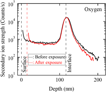
Figure 11. Depth profiles of oxygen concentration measured by SIMS before and after exposure to 10% ClF3 gas for one minute at room temperature.
Download figure:
Standard image High-resolution image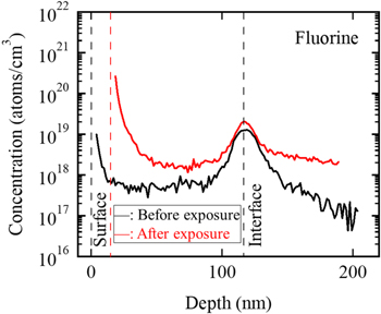
Figure 12. Depth profiles of fluorine concentration measured by SIMS before and after exposure to 10% ClF3 gas for one minute at room temperature.
Download figure:
Standard image High-resolution image
Figure 13. Depth profiles of chlorine concentration measured by SIMS before and after exposure to 10% ClF3 gas for one minute at room temperature.
Download figure:
Standard image High-resolution imageFigures 8, 9 and 10 show the depth profiles of the Si, C and N, respectively. As shown in these figures, the flat profiles of the Si, C and N concentration remained the same before and after exposure to the ClF3 gas. Thus, the ClF3 gas did not change the chemical conditions in the obtained SiCNO film.
As shown in Fig. 11, the oxygen had a peak at the interface between the obtained film and the aluminum substrate. This peak might be caused by the remaining aluminum native oxide film at the substrate surface. The oxygen concentration was flat in the obtained film before and after the exposure to the ClF3 gas. The oxygen concentrations near the surface were high before and after the exposure to the ClF3 gas, due to oxidation by storage in air.
As shown in Figs. 12 and 13, the fluorine and chlorine were contained in the film at the same position as that of oxygen. The fluorine and chlorine were considered to be emitted from the fluorocarbon resin around the electrodes in the reactor under the argon plasma prior to the film deposition. The fluorine and chlorine atoms were adsorbed at the aluminum substrate surface before initiating the deposition. By introducing the SiH3CH3 gas for the deposition, the fluorine and chlorine atoms were assumed to become the volatile products of silicon fluorides and the silicon chlorides in the gas phase. Thus, the fluorine and chlorine were not incorporated in the film, as shown in Figs. 12 and 13. While the fluorine concentration level seemed to be high after the exposure to the ClF3 gas in Fig. 12, the level in the substrate and that in the obtained film were the same in each profile. Thus, from Fig. 12, the fluorine concentration in the film was concluded not to be influenced by the exposure to the ClF3 gas. Due to the reaction with the ClF3 gas, the fluorine and chlorine concentrations near the surface were shown to increase.
Overall chemical process
The results obtained by the XPS and the SIMS were summarized. Based on the results obtained by the XPS, the surface of the film obtained by the PECVD was considered to consist of SiO2, Si–N, SiCO, C–C and SiCNO. After the exposure to the ClF3 gas, there were various species at the surface. While some of those, such as SiO2, Si–N, SiCO, C–C and SiCNO, were the original materials, an amount of these were significantly reduced. The others those existed at the surface were SiOx, Si–O, Si–C, C–N, C=N, C–O, C=O, O=C–O C–O–C, C–CFx C–Fx and C–Cl. These species could be classified into three groups. Group I is those less reactive or stable to the ClF3, such as SiOx, Si–O, Si–C, C–N, C=N. Group II is those oxidized after the exposure, such as C–O, C=O, O=C–O C–O–C. Group III is the fluorides and chlorides, such as C–CFx C–Fx and C–Cl, produced by the etching of the components containing carbon.
Figure 14 schematically shows the situation of the SiCNO surface. Figure 14a shows the materials contained in the obtained film. There are Si–N, C–C and C–O which are reactive with the ClF3. Additionally, the film contains the Groups I, II and III which are less reactive to the ClF3 gas. As shown in Fig. 14a, some amount of the reactive components, Si–N, C–C and C–O, exist at the surface. These are directly exposed to the ClF3 gas.

Figure 14. Schematic of SiCNO film situation (a) before and (b) after exposure to ClF3 gas. The thick dotted lines indicate the surface. I, II and III: Group number.
Download figure:
Standard image High-resolution imageAfter exposure to the ClF3 gas, the Si–N is changed into the volatile species of SiF4 and N2. 4 Thus, the position where the Si–N existed may become a shallow void to slightly change the surface morphology. Simultaneously, the C–C and C–O react to form C–F (Group II). Overall, because the reactive part is quickly removed, the top surface is consequently covered with the less-reactive components. Thus, about the corrosion by the ClF3 gas, while the SiN was very weak, the other components formed between the Si, C, N and O are less reactive and rather anti-corrosive. The etching behavior of the SiCNO film could be assumed as the chemical behavior of the various mixed components.
Next, the influence on the surface morphology is discussed. While the weak components were removed by the ClF3 gas, an actual surface morphology change was very small, as shown in Fig. 15. There were many parallel lines on the surfaces of the aluminum substrate and the obtained SiCNO film, shown in Figs. 15a and 15b, respectively. These lines still remained on the SiCNO film surface after the exposure to the 10% ClF3 gas, as shown in Fig. 15c. Figure 15 additionally showed that the sizes of dark spot, which might be small pits and particles, were similar among the aluminum substrate, obtained SiCNO film and that after the exposure to the 10% ClF3 gas. Thus, the SiCNO film surface morphology did not show obvious change, particularly for that formed on the non-polished aluminum substrate surface, shown in Fig. 15a.

Figure 15. Surface morphology of (a) aluminum substrate, (b) obtained SiCNO film and (c) SiCNO film after exposure to 10% ClF3 gas, by SEM. Dotted circles indicate dark spots.
Download figure:
Standard image High-resolution image
The etching of the reactive parts made the less reactive and anti-corrosive parts appear over the film surface, which were directly exposed to the ClF3 gas, as schematically shown in Fig. 14. The etching process was expected to be limited by the less reactive and anti-corrosive parts.
Conclusions
The anti-corrosive behavior of the SiCNO film formed by the PECVD with no heating was studied by an exposure to 10% ClF3 gas at atmospheric pressure. Due to the ClF3 gas, the Si–N components those existed at the surface were removed; the surface was fluorinated and chlorinated. As a result, the typical Si–C, Si–O and C–N components remained at the surface. Additionally, the Si, C, N and O concentrations in the film did not change. Thus, the SiCNO film could be anticorrosive ascribed to the nature of the components formed between four elements, Si, C, N and O, even when containing high nitrogen concentrations.