
Abstract
Material properties of Al-Sb binary alloy thin films deposited under ultra-high vacuum conditions were studied for multi-level phase change memory applications. Crystallization of this alloy was shown to occur in the temperature range of 180 °C–280 °C, with activation energy >2 eV. X-ray diffraction (XRD) from annealed alloy films indicates the formation of two crystalline phases, (i) an Al-doped A7 antimony phase, and (ii) a stable cubic AlSb phase. In-situ XRD analysis of these films show the AlSb phase crystalizes at a much higher temperature as compared to the A7 phase after annealing of the film to 650 °C. Mushroom cell structures formed with Al-Sb alloys on 120 nm TiN heater show a phase change material resistance switching behavior with reset/set resistance ratio >1000 under pulse measurements. TEM and in situ synchrotron XRD studies indicate fine nucleation grain sizes of ∼8–10 nm, and low elemental redistribution that is useful for improving reliability of the devices. These results indicate that Te-free Al-Sb binary alloys are possible candidates for analog PCM applications.
Export citation and abstract BibTeX RIS

This is an open access article distributed under the terms of the Creative Commons Attribution Non-Commercial No Derivatives 4.0 License (CC BY-NC-ND, http://creativecommons.org/licenses/by-nc-nd/4.0/), which permits non-commercial reuse, distribution, and reproduction in any medium, provided the original work is not changed in any way and is properly cited. For permission for commercial reuse, please email: permissions@ioppublishing.org.
Phase change materials (PCM) are being actively explored as analog resistive memory (memristive) devices for artificial intelligence applications. Currently, Ge2Sb2Te5 (GST) based films are the primary focus for PCM devices. 1 However, Te in GST can redistribute significantly during crystallization (set) and melt-quenched amorphous (reset) states due to its high volatility leading to reliability issues. 2,3 Te-free binary alloys of Sb with group III and IV elements have been studied as an alternative to GST. 4–6 Such materials demonstrate similar switching characteristics to GST but with improved stability. 5 Te-free Sb-rich materials also have been shown to have faster crystallization and a potential of lower power operations as compared to conventional GST based PCM. 7,8 The amorphous binary alloys made of group III-Sb alloys are of particular interest because these show multiple resistance plateaus during annealing of blanket Al-Sb films from 25 °C–300 °C. 6 The plateaus could facilitate the formation of metastable resistance states during reset/set switching thus allowing for multilevel data storage. 6 Additionally Al-doping in the PCM has been shown to improve thermal stability. 9,10 Furthermore, the composition Ga0.3Sb0.7 shows zero volume change during set/reset cycles unlike GST devices that undergo ∼6.5% volume change during set/reset cycling, contributing to premature device failure. 4 This work explores Te-free Al-Sb alloys with various Al compositions for phase change memory devices and their potential for multilevel, analog data storage. 11 In particular, these materials are well-suited for multilayer structures where layers of PCM alloys with different crystallization temperatures are assembled to provide multiple resistance states. 12,13
Materials and Methods
Al-Sb amorphous layers were deposited by molecular beam epitaxy (MBE) under ultra-high vacuum of ∼7 × 10⁻¹¹ Torr at 20 °C on a Si (100) substrate with 1 μm thick, thermally grown SiO2. The film compositions were measured by an in situ Auger electron spectroscopy (AES). These films were capped with a 20 nm of Al2O3 to prevent oxidation of the Al-Sb alloys. PCM confined cells with a 0.2 and 1 μm wide via were prepared on Si3N4/TiN/p + Si template using e-beam lithography. Similarly PCM mushroom cell devices with 120 nm TiN heater were fabricated in the SUNY Polytechnic Institute 300 mm Si foundry. Al-Sb layers of thickness 20–200 nm, as well as 200 nm top Al contact were deposited using MBE at room temperature. For mushroom cell devices 30–50 nm top TaN electrode was in situ deposited using sputtering in ultra-high vacuum (UHV) connected separate chamber. PCM cells were completed with optical lithography and dry/wet etching of top contact pads and PCM layers to separate individual devices.
The crystallization of as-deposited amorphous Al-Sb alloy films was performed on a hot plate in air and the change in resistance as a function of temperature was measured with a two-point probe setup at a constant temperature rate. The sample resistivity was obtained by the van der Pauw method. The crystallization temperature and activation energy were determined from the resistance vs temperature curves. The same setup was employed to evaluate resistance drop with annealing time at a fixed temperature for obtaining data retention. In situ (synchrotron) and ex situ XRD methods were used to study the nucleation and crystallization behavior of Al-Sb alloys. This included obtaining the phase information of the crystallites as well as their relative fraction in the Al-Sb alloy. Transmission electron microscopy (TEM) provided quantitative information on the grain size, crystallization behavior, and redistribution of elements. Electrical testing demonstrating reversible switching of Al-Sb confined cells was performed using Keysight pulse generator for cell switching and source-measure unit to characterize the PCM cell resistance.
Results and Discussions
Thermo-electrical analysis
Figure 1a shows sheet resistance as a function of temperature for 160 nm thick Al-Sb films with different Al concentration. The as-deposited samples were amorphous with initial resistance ranging from 105 ohm/sq. to 109 ohm/sq. for 10 at% Al to 45 at% Al, respectively. There was a gradual exponential drop in the sheet resistance with increasing temperature followed by a sharp drop at crystallization temperature. The final sheet resistance was dependent on the Al content in the alloy: ∼5 × 10³ ohm sq−1 for Al0.45Sb0.55 and ∼102 ohm/sq for Al0.1Sb0.9. Samples with 10%–30% Al exhibited distinct resistance plateaus just before the crystallization temperature, which agrees with the previously published results. 6 This phenomenon has been attributed to improved crystallization without any additional phase transformation. 6 Although the mechanism of these metastable plateaus is not clear, it was shown to be reproducible. It is possible that these plateaus may improve stability of multiple resistance states in memory devices.

Figure 1. (a) Resistance as a function of temperature of as-grown amorphous Al-Sb alloys with variable Al fraction for a heating rate of 5 °C min−1 and subsequent cooling to room temperature. (b) Crystallization temperature dependence on Al content at various heating rates. The temperature corresponding to an abrupt resistance change before and after a resistance plateau are shown with open and solid symbols, respectively. Crystallization temperatures of GST PCM alloy is shown for comparison. (c) The Kissinger plots showing slopes corresponding to activation energies for crystallization (Ea) for high-temperature transition in samples with different Al fractions. (d) Arrhenius extrapolation at 10-years of data retention.
Download figure:
Standard image High-resolution imageThe dependence of two crystallization temperatures, corresponding to low-T (metastable) and high-T resistance drops, on Al content at various heating rates is shown in Fig. 1b. For comparison, similar values for GST films prepared by room temperature sputtering from stoichiometric target at room temperature are shown. It is evident that the crystallization temperature TC increases with Al% reaching a maximum value of 270 °C at 30% followed by a decrease in Tc at higher Al%. Essentially Al bonding leads to an increase in total bond enthalpy leading to an increase in glass transition temperature that has been shown to be proportional to high crystallization temperature. 9 The TC for all Al% is noticeably higher than that for GST (173 °C–188 °C) which is expected to result in higher thermal stability for Al-Sb based PCM devices. Observed TC also shifted to higher temperature with the heating ramp rate; this TC shift is used to derive activation energy for crystallization using the Kissinger method. 14 The activation energies obtained from Fig. 1c range from 1.8–2.8 eV which are quite similar to that obtained for GST alloys. Figure 1d shows extrapolated failure time for Al-Sb PCM devices. It is clear that high activation energy of Al0.2Sb0.8 and Al0.3Sb0.7 alloys will allow improved data retention at 138 °C and 169 °C for 10 years. This 10-year projected data retention is similar to what has been shown previously for Al based PCM. 10,15
Phase structure of the Al-Sb PCM alloys
Figure 2a shows crystalline phases of 300 °C annealed Al-Sb films using grazing-incidence XRD. The absence of any distinct diffraction peaks in the spectra from the as-deposited films (not shown) indicates that this material is amorphous which is consistent with previously published results. 4,6,13 The annealed films consisted of only two crystalline phases, namely rhombohedral Sb (A7) phase 16 and cubic zinc-blende AlSb phase as confirmed by simulations (Fig. 2a). The relative fraction of the cubic AlSb phase increases along with increasing Al% as evident from the disappearance of diffraction peaks corresponding to the A7 phase. To quantify the relative volume of the two phases in the films, areas under the (111) AlSb and (012) A7 peaks were obtained from the diffraction data and compared with the simulated volumes under these peaks (using scattering and structure factors) as shown in Fig. 2b. To improve the accuracy of calculations, areas under weaker peaks such as (002) and (101) were also taken into consideration. Comparison of experimental and simulated data indicates that the rhombohedral Sb phase can contain up to 10–15 at.% of Al which is much higher than the equilibrium solubility of Al in Sb at its melting point of 630 0C (∼ 2 at.%). 17 It can be summarized that non-equilibrium Sb A7 phase forms exist in the low-resistance state of Al-Sb alloys.

Figure 2. (a) Grazing angle XRD patterns of Al-Sb films with variable Al concentration annealed at 300 °C. Two simulated patterns are shown for Sb A7 phase (bottom) and zinc-blende AlSb phase (top). Vertical dashed lines indicate the strongest peaks. (b) Volume ratios of zinc-blende AlSb phase calculated from the XRD patterns. Lines present the expected AlSb volumes when the solubility of Al in A7 Sb phase is 5,10,15 and 20%.
Download figure:
Standard image High-resolution imageCrystallization of phases after melting of Al-Sb PCM alloys
Al-Sb alloys based PCMs are two phase system consisting of rhombohedral A7 and AlSb cubic phase as shown earlier by XRD results. In-situ XRD analysis was also done on these alloys to further understand the crystallization behavior upon heating and recrystallization after melting. Figures 3a and 3b also confirm the two phases for both Al0.2Sb0.8 and Al0.3Sb0.7 alloys upon heating to 500 °C. Figures 3a and 3b both show the peaks intensity getting strong for both A7 and cubic phase that suggests grain growth as also shown later in Fig. 5d. The two films were further annealed close to their melting temperatures and then were cooled down to room temperature. Figures 3c and 3d show the color plot of crystallization of the films upon cooling from melting. Both of the alloys show that the A7 phase crystalizes at a different temperature as compared to the cubic phase which stays crystalline even after annealing to 650 °C. Figure 3e further confirms this behavior as the intensity profile corresponding to 631 °C is missing the (012) peak and it starts to appear around 600 °C while the peaks corresponding to cubic phase are present for all the temperatures. These results mean that the AlSb phase crystallizes at a much higher temperature as compared to the A7 phase which can conclude that resistive switching of this two-phase system is mostly due to the crystallization of only the Sb A7 phase.
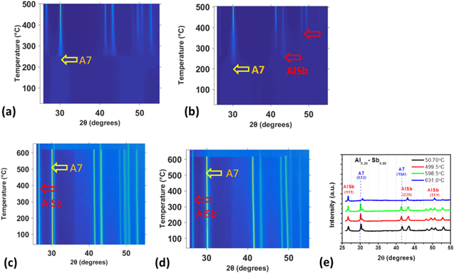
Figure 3. In-situ Synchrotron XRD patterns of Al-Sb films with variable Al concentration. (a) In-situ XRD pattern for Al0.2 Sb0.8 film annealed to 650 °C. (b) In-situ XRD pattern for Al0.3Sb0.7 film annealed to 650 °C. (c), (d) XRD pattern showing recrystallization after melting for Al0.2 Sb0.8 and Al0.3Sb0.7 respectively. (e) Intensity profile of the Al0.2Sb0.8 film for different temperatures after the high temperature anneal, this is the same film as shown in Fig. 3c.
Download figure:
Standard image High-resolution imagePulse measurements
Al-Sb alloy was used as a phase change layer in PCM mushroom cells to evaluate its electrical properties. Figure 4a presents the fixed pulse width programming R-V characteristics from reset state of 20 nm thick Al0.3Sb0.7 film deposited in amorphous state on a 120 nm TiN heater and capped with in situ deposited TaN electrode. With the increase of pulse amplitude the low resistance set state appears for pulse voltage as small as ∼1.2 V for different pulse widths. With further increase in pulse amplitude the resistance returns to the high resistance reset state. Al0.3Sb0.7 shows larger resistance contrast with similar pulse parameters compared to other Al doped Sb-rich PCM materials. 10,13,15 The set and reset operation of Al-Sb based device requires pulses with lower amplitude than what has been shown for conventional GST 18,19 which can lead to lower power consumption in Al-Sb cells. Higher reset resistance of Al-Sb alloy plays an important role in reducing the energy for set and read operation and also leading to low power consumption. It should be noted, that the over half of the volume of the Al0.3Sb0.7 alloy consists of cubic AlSb phase which is semiconductor with a relatively wide bulk bandgap of 1.6 eV that can be larger due to the effect of crystalline confinement. Due to the large AlSb bandgap the Al-Sb alloy may be expected to constitute a highly resistive matrix. Figure 4b presents reversible switching properties of Al-Sb based mushroom cell. A very high reset/set resistance ratio of >1000 was observed on Al0.3Sb0.7 cells as compared to ∼100–500 for GST. 15,18,20 Te-poor PCM has also been shown to have low resistance contrast, 21 and this three orders of magnitude resistance change for Te-free Al-Sb alloy based PCM shows a great promise toward providing an adequate margin for programming multiple resistance states for multileveled storage devices. The randomness in the set and the reset state can be reduced by better pulse programming and by introducing a metal nitride liner as a drift stabilizer. 22 This large resistance contrast and potential for lower power consumption makes Al-Sb alloys a promising candidate for analog memory application devices.
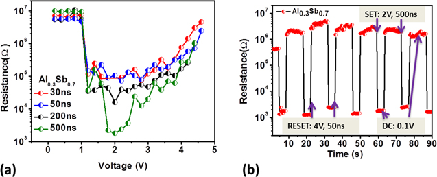
Figure 4. (a) R-V performance of 20 nm thick Al0.3Sb0.7 PCM mushroom cell with TaN top electrode for different pulse widths with rising and trailing edge width of 10 ns. (b) Reversible switching characteristics of Al0.3Sb0.7 mushroom cell device demonstrating resistance contrast over 3 orders of magnitude.
Download figure:
Standard image High-resolution imageChanges of the PCM alloy microstructure and chemical stability after switching
Dark-field cross section TEM of a confined cell (Fig. 5a) shows fine crystalline grains in the device region where the switching occurred after ∼100 reversible switching cycles when the device was left in the low resistance set state. It should be noted, that the cell with Al top electrode typically failed after a few hundred cycles likely due to low chemical stability of Al/Al-Sb interfaces and/or Al electromigration. Replacement of the top electrode with TaN improved endurance to at least 106 cycles which will be discussed elsewhere. However, even with the relatively unstable Al electrode the microstructure and chemistry are not affected significantly by Al mass transport as shown below. The polycrystalline granular structure is also visible in Al0.3Sb0.7 layer over the Si3N4 film which extends up to ∼0.5 μm from the active device region, presumably due to excess heating during the switching. A histogram of grain sizes is shown in Fig. 5c with an average grain size of ∼ 8 nm.
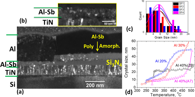
Figure 5. (a) A cross-sectional dark field (DF) TEM image of a 40 nm Al0.3Sb0.7 PCM layer in a 1 μm confined cell in set state after ∼100 cycles switching. (b) Magnified DF image showing grains in Al-Sb and TiN. (c) Histograms of grain sizes obtained from four DF images. (d) Crystal size evolution with temperature from in situ synchrotron measurements of XRD FWHM reflections using Scherrer method: (012) for A7 phase and (111) for zinc-blende AlSb phase.
Download figure:
Standard image High-resolution imageThe evolution of the crystalline grain size in blanket films of Al20%, 30%, and 40% during annealing from 200 °C–500 °C was also obtained by in situ synchrotron XRD measurements (Fig. 5d). Figure 5d reveals two distinct onsets: Firstly corresponding to nucleation with relatively wide temperature range of unchanged grain size and secondly implying grain growth. The grain growth of both Sb A7 and cubic AlSb phases were obtained for Al0.4Sb0.6. There is very little change in the grain size of the Sb A7 phase crystallites up to 450 °C (from 5–10 nm) but the grain size increases sharply by a factor of 4–5 in the temperature range of 450 °C–500 °C. Crystallites composed of cubic zinc blende (ZB) AlSb phase, however, do not show any appreciable grain growth even up to 500 °C. This is attributed to the high 1065 °C melting point of cubic AlSb. Since the AlSb grain stays stable upon annealing, this suggests that grain growth is due to agglomeration of A7 Sb grains. The resistance change during switching is therefore dominated by the Sb A7 phase crystallites rather than cubic AlSb crystallites.
Figure 6 illustrates redistribution of Al and Sb in the Al0.3Sb0.7 confined cell after ∼100 cycles switching. Al Kα and Sb Lα line intensity profiles were obtained by energy dispersive X-ray spectroscopy (EDX) from a cross-section TEM sample of a PCM device (Figs. 6a and 6b). The profiles across the Al-Sb layer on TiN (inside the cell) and Si3N4 (1 μm away from the cell) show a change of Al profile across the PCM layer thickness (Fig. 6c). The 2x change of Al fraction slope across the layer thickness is quiet prominent and could likely be an influence of thick Al contact. The change in Al-Sb composition is significantly less than in typical Te-containing GST alloys2, indicating higher chemical stability of Al-Sb PCM materials.

Figure 6. STEM high angle annular dark field images of 40 nm thick Al0.3Sb0.7 layer (a) on a TiN heater contact inside PCM cell switched multiple times, and (b) on Si3N4 dielectric about 1 μm away from the cell. (c) Al Kα and Sb Lα EDX line intensity profiles across the Al-Sb layer on TiN and Si3N4 (in the centers of the images) showing a visible change of Al content across the PCM layer thickness.
Download figure:
Standard image High-resolution image
Conclusions
The Al-Sb binary alloy material system shows potential for analog phase change memory applications and was demonstrated to undergo phase change resistive switching. The controllable high crystallization temperature ranges from 180 °C–280 °C and high activation energy up to 2.8 eV, and retention up to 169 °C for 10 years for these films, indicates thermal stability and potential for reliability. XRD studies showed crystallization into two phases, Al-doped A7 antimony and cubic AlSb. Further in situ XRD studies show that the resistive switching of these alloys is possibly due to recrystallization of the A7 phase since the cubic phase stays crystalline even after high temperature anneal. Reversible switching was also shown with reset/set resistance ratio of >1000 with reset switching times as low as 50 ns. The TEM, EDS and in situ synchrotron XRD data showed fine grain sizes of 8–10 nm corresponding to nucleation rather than growth phases, and low elemental redistribution that is useful for improving reliability of the devices. These results indicate that Te-free Al-Sb binary alloys with simple chemistry are possible candidates for high speed, analog PCM applications.
Acknowledgments
This work was supported by the Semiconductor Research Corporation (Task 2960) and the SUNY-IBM AI Collaborative Research Alliance.