
Abstract
This paper reviews the topic of the device parameter variations using semiconductor-based manufacturing of micro- and nano-devices. There is considerable misunderstanding about the precision of these types of manufacturing methods and that smaller does not always mean more precise. This issue is very important to many types of devices made using semiconductor manufacturing, particularly those having analog functionality including MEMS, NEMS, photonics, analog ICs, and nanotechnologies. It also is getting increased attention in digital ICs as the gate lengths have decreased. It is shown that the relative variations using these manufacturing methods are generally larger in magnitude compared to more conventional methods of production such as traditional machining operations. Moreover, since many of the devices made using semiconductor-based manufacturing methods have analog-functionality, device parameter variations can have a magnified impact on the variations exhibited in the device output behavior. Methods to estimate the impact of device parameter variations on the device output behavior are given, including an analytical method and Monte Carlo analysis. The impact of these variations on the manufacturing yield is explained and demonstrated. Lastly, a number of techniques that can be used to manage these device parameter variations so as to improve the manufacturing yield are given.
Export citation and abstract BibTeX RIS

This is an open access article distributed under the terms of the Creative Commons Attribution Non-Commercial No Derivatives 4.0 License (CC BY-NC-ND, http://creativecommons.org/licenses/by-nc-nd/4.0/), which permits non-commercial reuse, distribution, and reproduction in any medium, provided the original work is not changed in any way and is properly cited. For permission for commercial reuse, please email: permissions@ioppublishing.org.
From the discovery of the transistor in 1947 to the present day, semiconductor-based manufacturing has advanced at an amazing rapid pace resulting in tremendous societal benefits for the world's population. Early progress was driven by the recognition that discrete electronic devices made from semiconductor materials significantly outperformed the existing vacuum tubes. Subsequently, it was realized that printed boards wired with discrete components could be replaced by integrated circuits (ICs) wherein various electronic devices, including transistors, resistors and capacitors, could be fabricated directly into semiconductor substrates made from silicon, thereby resulting in much lower costs, smaller sizes and weights, better performance, and higher reliability. IC manufacturing is now an extremely sophisticated technology used to implement tens of billions of transistors on each die (i.e., microchip) for the production of highly advanced systems. IC devices are now used in almost every type of industry and product that processes, communicates and/or stores information.
The technological, economic, and societal impact of semiconductor manufacturing continues to grow and has become increasingly more diverse, resulting in significant successes in other types of micro- and nano-fabricated device technologies. 1 Specifically, semiconductor manufacturing is now being used to implement a broad spectrum of different technologies, including: integrated circuits made in non-silicon substrates (e.g., Gallium Arsenide (GaAs), Gallium Nitride (GaN), Silicon Carbide (SiC)); micro-electro-mechanical systems (MEMS) and nano-electro-mechanical systems (NEMS); photonics; vacuum electronics; microfluidics; lab-on-a-chip; and a multiplicity of nanotechnologies. Sometimes, these technologies are differentiated into the category of micro- or nano-systems, depending on the dimensional size scale of the critical features. Nevertheless, all of these technologies share many of the same semiconductor-based fabrication techniques including: deposition, lithography, etching, and metrology.
One issue in semiconductor manufacturing that has received relatively little attention in most non-IC technologies relates to the device parameter variations that result from the use of these fabrication methods. Device parameter variations are the differences in the device parameter values (i.e., the dimensions and material properties) of the critical elements of the devices from the desired values of these same parameters. The desired values of the device parameters are usually established during the device design in order to meet the application requirements. A major reason why this issue has not received much attention is partly due to the fact that semiconductor-based manufacturing has been dominated by digital ICs that are comparatively far less sensitive to device parameter variations compared to other technologies, such as MEMS, NEMS, analog-circuits, photonics, etc., that use analog-based functionality. However, as the sizes of the gates in ICs have steadily decreased, parameter variations in digital circuits are increasingly becoming an important issue. 2 Furthermore, the continued growth of other technologies, such MEMS, NEMS, photonics, and radio-frequency (RF) ICs, has made it essential for designers and fabricators to address parameter variations resulting from the use of semiconductor-based manufacturing methods in order to obtain adequate performance and/or yields.
There is considerable misunderstanding about this topic. It is often stated that the semiconductor-based manufacturing methods provide for high levels of dimensional "precision" compared to macro-scale production methods, such as conventional machining. This is not true in most circumstances. While semiconductor-based manufacturing can enable the dimensions to be made very small, that is not the same as fabricating them with a high degree of precision. Additionally, it is useful to note that accuracy and precision are both important with respect to parameter variations in these technologies. The topic of manufacturing parameter variations is relevant to the dimensional parameters of devices and systems, and it is also relevant to the material properties since they both have an impact on the resultant device behavior. Therefore, the resultant variations of both the dimensions and material properties should be considered during design. Given the relatively large variations in device parameters involved in semiconductor-based manufacturing, this issue has a significant impact on yield.
It is important to consider the physical equations describing the device's behavior since these often involve one or more of the device's dimensional parameters raised to higher powers (e.g., squared, cubed, quartic). This significantly increases the impact on the device behavior for analog-functioning devices.
The topic of this paper is to highlight the importance of parameter variations in semiconductor manufacturing, followed by an explanation of the techniques that can be used to estimate and manage the device parameter variations resulting from the use of these fabrication methods. The material in this review paper is covered in far more detail in a recently released volume entitled: "Process Variations in Microsystems Manufacturing." 3
Prior Work on Process-Induced Parameter Variations:
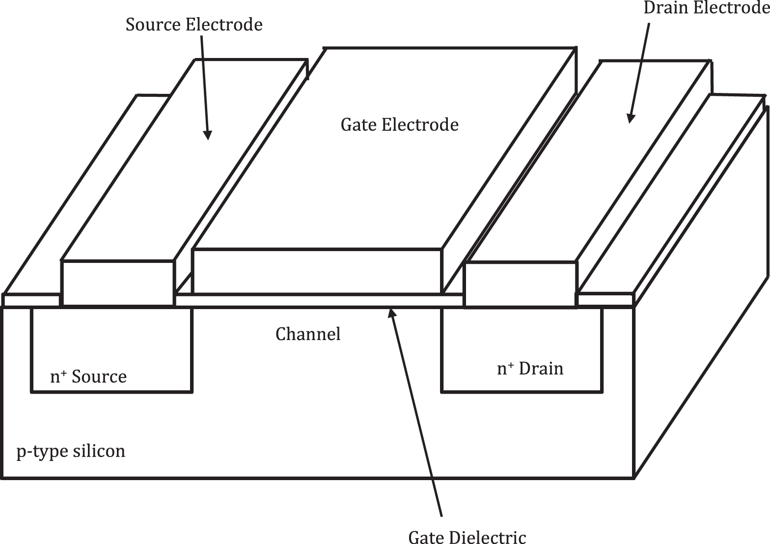
By far, the most common semiconductor-based device made is the metal-oxide semiconductor field effect transistor (MOSFET) 4 and the most widely used configuration combines n-channel and p-channel MOSFET devices together to form complementary metal-oxide semiconductor or CMOS integrated circuits. The three electrode terminals of the MOSFET are the source, drain, and gate (Fig. 1). A voltage potential across the source and drain regions can cause current to flow through the device channel depending on the applied voltage on the gate, which is electrically isolated from the channel by a gate dielectric. Voltages applied to the gate can close, open or partly open the flow of current through the channel.
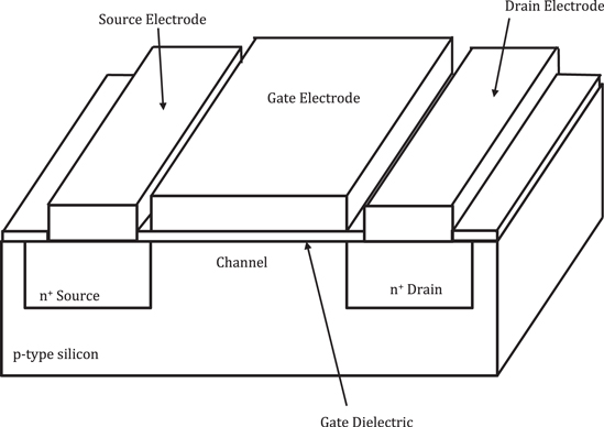
Figure 1. Cross-section of a n-channel MOSFET device. 4
Download figure:
Standard image High-resolution imageThe three regions of operation are: the cut-off region where device is "off"; the linear region where drain current is proportional to the channel resistance; and the saturation region where drain current is almost constant. The current through a MOSFET transistor, ID (units Amps), in the linear active region is given by: 4

where μ is the charge carrier mobility (m/V sec), Cox is the capacitance of the gate (F/m), W is the gate width (m), L is the gate length (m), VGS is the gate to source voltage potential (V), VT is the threshold voltage (V), and VDS is the drain to source voltage potential (V). In analog applications, the MOS transistor is usually operated in the linear region. In digital applications, the transistor is turned "on" and "off" with the device being in the cut-off region, "off," or the linear region "on."
Process-induced device parameter variations using semiconductor-based manufacturing have been a research interest in integrated circuits (ICs) since the early days of the technology. One of the first articles on this subject was in 1961 by Shockley who reported the fluctuations in the junction breakdown voltages of diodes. 5 The effects of systematic variations in MOSFETS were first reported in 1974 in a study of the sensitivity of the threshold voltages as a function of implant energies and gate oxide thicknesses. 6 This work was later expanded and applied to MOSFET devices to model the effects of random variations in the number of dopant atoms in the depletion region of the device. 7
Much of this early work was directed at ICs having analog functionality where the physics make the behavior of the transistors much more sensitive to process variations. Digital CMOS rapidly replaced most analog ICs partly due to the fact that switches are either "on" or "off," and therefore, are far less susceptible to parameter variations. Nevertheless, as the integrated circuit industry has rapidly grown and developed more advanced production methods to enable the continuous shrinking of devices and their critical dimensions, process variations are increasingly becoming a very important topic in advanced digital ICs (See Fig. 2). Borkar and Springer provided general overviews of this subject as it relates to planar bulk silicon CMOS integrated circuits. 8,9 Kuhn also provided a review on the topic process variations for CMOS technologies using the standard CMOS device layouts at the 45 nm node 10 and Champac gave a through review of effects of process variations on nanometer digital circuits. 2
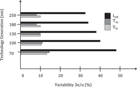
Figure 2. Variations in channel length, Leff; gate oxide thickness, Tox; and threshold voltage, Vth; for several generations of IC technologies. 11
Download figure:
Standard image High-resolution imageThe main sources of process variations of planar MOSFETS are in the channel lengths and are usually considered to be due to the photolithography and etching steps, 12,13 specifically resulting in line edge roughness 14 and optical proximity effects. 15 Line edge roughness is self-explanatory and refers to the roughness of the edges of the gate in the MOSFET device. 2,16–20 Optical proximity effects are the changes in the sizes and shapes of patterns being transferred in photolithography based on the proximity of these patterns and are due to diffraction effects when using exposure wavelengths that are multiples of the features being transferred. 13,15,16 These effects result in features that are closely bunched together having different sizes and shapes compared to the same sized features that are isolated. Optical proximity correction is used to partly mitigate the effects of OPE. 16,21 The variation in the channel width usually has a lesser impact on the device behavior than the length due to the fact that the width is considerably larger in dimension. The dimensional variations in the channel width are mostly due to the same reasons as the length, namely edge line roughness and optical proximity effects. Additionally, photolithographic mis-alignment is also a source for variation of the channel width. 22,23 The gate dielectric thickness variations can also be impactful, 24–28 as the gate dielectric thicknesses have decreased with the scaling of MOSFET devices to only about 16 nm in 22 nm devices. 2
Additionally, as the device size has decreased along with an accompanying decrease in gate dielectric thickness, leakage currents have caused manufacturers to replace silicon-dioxide as the preferred gate dielectric material with materials having higher dielectric constants. 29,30 While the thickness control and uniformity of gate dielectric deposition processes have not degraded, since the thicknesses are now so small, on a relative basis the variations have increased. 2,31 Variations in the threshold voltages of MOSFET devices are due to the gate material, gate thickness, and dopant concentrations, with the variations in the dopant concentrations reported as the largest contributing factor. This is often termed as random dopant fluctuations and it increases as the channel length decreases. 32–40 Other sources of variations in MOSFETs include: fixed and trapped charges; 41–47 chemical-mechanical polishing; 48–54 strain levels; 55–61 as well as due to the specific processing steps used in manufacturing. 62–67
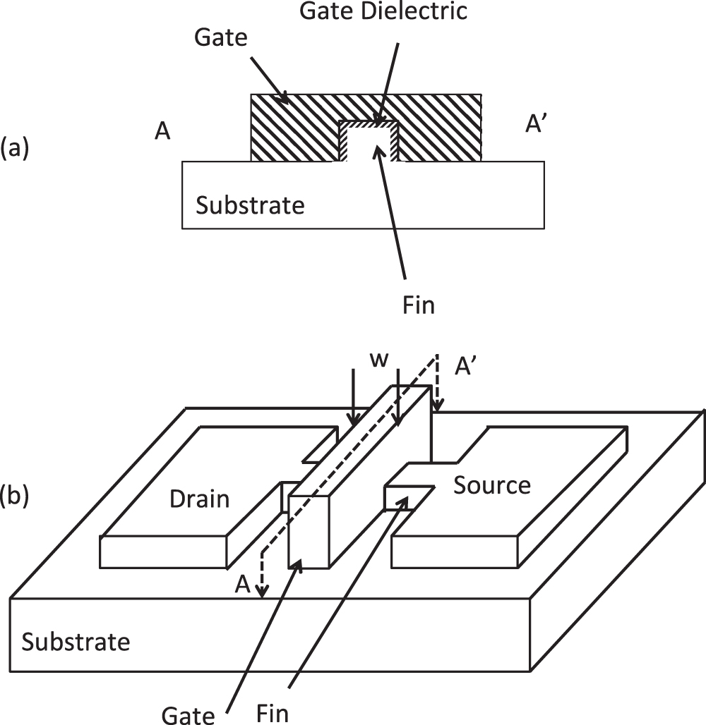
While planar CMOS has been the standard device configuration for a number of generators of IC technologies, once the gate sizes decreased to the 22 nm technology node the planar structure was replaced by the FinFET technology illustrated in Fig. 3. 2,68–70 FinFET transistor technology is now exclusively used in the manufacturing of state-of-the-art integrated circuits from 22 nm down to 10 nm and 5 nm, and 3 nm preliminary devices have been reported. 70

Figure 3. An illustration of the FinFET transistor. Shown in (b) is a 3-D representation of an individual FinFET transistor with a single fin. The source, drain and fin are all made from single crystal silicon. The fin is a high-aspect ratio channel connecting the source and drain where the charge carriers can flow. As shown in (a), the fin is coated in the thin dielectric layer and then with the gate material layer, which is an electrically conductive material. Since the voltage on the gate creates and electrical field on both sides and the top, this configuration is also called the "tri-gate" transistor.
Download figure:
Standard image High-resolution imageA FinFET is a non-planar metal-oxide semiconductor (MOS) transistor technology having the notable attribute of a fin of single crystal silicon semiconductor material that has a relatively high aspect ratio that protrudes from the substrate surface. 2 Like a conventional MOS transistor there is a source, drain and gate. However, unlike a conventional MOS device, the source and drain are connected by a thin, high-aspect ratio (height is larger than the width), fin of silicon. The fin acts as the channel for the flow of charge carriers from the source to the drain that is modulated by the gate voltage potential. The gate overlaps the fin and has a very thin dielectric to insulate the gate electrode from the fin. The gate overlaps the fin on three-sides, the top and the two sides. Consequently, this structure is also called a "tri-gate" structure. This tri-gate configuration allows the gate voltage to have improved control capability over charge carriers in the channel. 2
There are also sources of process-induced parameter variations in FinFETs. 2,14,71–73 One source is the gate work function variation, which is the difference between the work function of the gate and the semiconductor materials and is due to the use of metal gates that have variable work functions depending on the random occurring grain orientations. 71,74,75 Another source of process variation is line edge roughness, which is due to many of the same reasons as planar devices including: photolithography and etching variations across the wafers. 76–80 Both effects increase on a relative basis as the gate lengths have decreased. 2 Random dopant fluctuations are another source of variation and has been minimized by using un-doped or slightly doped regions. 76 The height of the fins is another source of variation. 77
As can be appreciated by a review of the prior work above, there have been a number of investigations of the process-induced device parameter variations involved in IC manufacturing. One reason is that IC manufacturing is very large and mature. Another reason is that IC manufacturing essentially makes only three types of components, namely transistors; capacitors; and resistors. Therefore, the research has been able to remain focused on a relatively small number of issues related to process variations, such as line edge roughness, gate oxide thickness, and random dopant fluctuations; even as the industry has progressed with each new generation of IC technology.
The situation for other types of devices made using semiconductor-based manufacturing methods is very different. These industries tend to be vastly smaller than the IC industry and also far less mature since they are based on more recent developments. Moreover, the configuration, process sequences used for implementation, and physics tend to vary greatly from device to device. For example, MEMS and NEMS technologies span an enormously vast array of different and diverse device technologies including: pressure sensors; inertial sensors; magnetic sensors; light sensors; infrared sensors; microfluidic; micropumps; microvalves; lab-on-a-chip; digital light displays, and many more. 3 Each of these device types will usually have its own unique process sequence. Additionally, many of these technologies, such as MEMS and NEMS, have mechanical and/or electromechanical functionality and therefore have behavior that is more susceptible to process-induced parameter variations and generally require higher levels of manufacturing precision. 81 As a consequence, there has been a very sparse amount of reported research on process variations for non-IC device technologies and the work reported to date is focused on dimensional process variation for a specific device type, such as surface micromachined resonators. 82 More useful generalized methods of analysis and methods for managing these process-induced device parameter variations are needed. 3
Semiconductor-Based Manufacturing Methods
Semiconductor-based manufacturing entails performing a series of sequentially executed processing steps (See Fig. 4). There are hundreds of individual processing steps available for implementation. These processing steps can be organized into categories and placed into a hierarchy of relationships, such as thin-film depositions and growths; lithography; etching; wafer bonding; chemical mechanical polishing; substrate cleaning; impurity doping; and others. 3
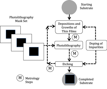
Figure 4. Flow chart illustrating semiconductor-based manufacturing composed of major processing step group types such as thin film depositions, lithography, etching, impurity doping and metrology (Metrology can also encompass inspection of the wafers during manufacturing). The major processing group types are often repeated several times in a process sequence using different sub-categories of processing steps and materials.
Download figure:
Standard image High-resolution imageEach of these broad categories can be further broken into sub-categories. For example, under thin-film depositions or growths can be listed: chemical-vapor deposition (CVD); physical-vapor deposition (PVD); oxidation; spin-casting; lamination; and others. These sub-categories can be further partitioned, as for example the sub-category of chemical-vapor deposition can be further differentiated as: low-pressure chemical vapor deposition (LPCVD); atmospheric pressure chemical vapor deposition (APCVD); plasma-enhanced chemical vapor deposition (PECVD); atomic layer deposition (ALD); and others. A hierarchical categorization is shown in Fig. 5. The individual processing steps are normally performed on specialized commercially-available process equipment.
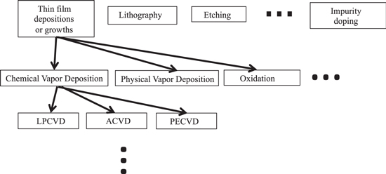
Figure 5. Illustration of the categorization of semiconductor-based processing steps used in manufacturing. Shown is a partial breakdown of the processing steps under the category of thin film deposition and growths.
Download figure:
Standard image High-resolution imageA multiplicity of processing steps is used to implement the devices. Individual processing steps arranged into an ordered array of sequentially performed steps that collectively result in functional devices is called a process sequence. 3 The selection and ordering of the processing steps is dependent on what is being implemented. Different types of devices commonly use different types of processing steps having unique ordering of the processing steps for their fabrication. If the process sequence is sufficiently developed and matured in a manufacturing environment, it may be referred to as a process technology. Process technologies often have design rules that facilitate successful design. The focus of this paper is not on the mechanisms or descriptions of processing steps or process sequences used in semiconductor manufacturing, but instead on the device parameter variations resulting from the use of these manufacturing methods. There are a number of excellent resources on the physics, chemistry and equipment used in performing processing steps available to interested readers. 3,83–87
The process-induced critical device parameters will vary from one device type to another since different device types will have different configurations, designs, and process sequences. Therefore, the designers need to be able to estimate the expected process variations depending on the process sequence and device design. There are sources available that provide useful guidance on the variations of individual processing steps. 3,84,85 However, it should be noted that estimating the amount of process-induced parameter variations resulting from the process sequence is a more challenging endeavor. The amount of variation of a photolithography processing step performed on a perfectly flat surface using a specific tool and technology is usually known. Likewise, information about the non-uniformity of a thin-film deposition or etch using a specific tool and technology is usually also known, at least for particular material systems. However, using that information to estimate the process variations when there are a large number (tens to hundreds) of individual processing steps is far more difficult since layers do not exactly align to one-another, there are overlaps where the thin-film layers have sloping profiles, the photolithography may be in or out of focus depending on the location on the substrate and the surface topography, etc. Highly experienced fabrication engineers are able to make reasonable estimates of the resulting process variations from a process sequence, but this must be validated with actual fabricated devices. But it is important to note that many non-IC micro- and nanodevices are made using customized process sequences and therefore a priori knowledge of the process variations is usually not available. 3
Most semiconductor manufacturing is based on the important production concept called batch fabrication whereby the processing steps are simultaneously performed on a batch (also sometimes called a "lot") of substrates. Each of the substrates usually contains hundreds to thousands of individual die depending on the diameter of the substrates and the area of the die. Using the batch fabrication model, multiple batches of substrates can be concurrently involved in manufacturing, with different batches located at different processing steps (i.e., work stations) in the process sequence. The substrates (also called "wafers") typically have standardized diameters and thicknesses. This standardization is important since the equipment used is sized according to these standards. Batch fabrication is an extremely important manufacturing advantage since it allows a large number of die to be simultaneously produced, thereby, resulting in relatively low per die production costs.
The dimensions of the critical features of semiconductor-based devices are often of primary interest and used as a means of comparing different technologies. Smaller critical feature sizes usually imply the use of more advanced fabrication techniques as well as the ability to place more devices on each die, and more die on each substrate. What is deemed as the critical feature of a device depends on the type of device being made. In IC technologies, it is usually the gate length of the transistors that is considered the most important feature size. 2 The digital IC industry has been reducing the size of gate lengths of transistors and increasing the number of transistors on each die steadily over several decades (i.e., the so-called "Moore's Law"). Current state-of-the-art IC manufacturing processes are now able to make gate lengths below 10 nm and hundreds of millions of transistors on each die. 8,70
While the reduction in minimum feature sizes is a key driver in most digital IC manufacturing environments, the situation is more complex for other technologies. The physics of many of these devices may dictate that larger sizes are preferable. For example, an inertial microsensor may need a specific amount of mass and sidewall capacitance in order to be able to be sufficiently sensitive to acceleration changes, and this may require that the dimensions are relatively large compared to what is state-of-the-art in IC manufacturing. For this reason and others, many of the non-IC and non-silicon-based semiconductor technologies often have considerably larger dimensions than advanced digital ICs.
The Importance of Parameter Variations
No manufacturing process is perfectly repeatable where each item made is an exact copy of the others, or can absolutely replicate the parameter values (i.e., dimensions and material properties) specified in the design. A device parameter variation is defined as the difference between the desired value of the parameter and the resultant value of the parameter after the manufacturing has been performed. The desired value is usually established during the device design. The consequence of these device parameter variations is that when they deviate from their "as-designed" values the output of the device will also exhibit a variation in its behavior. Further, these variations in the device output may result in the device not working or not meeting the required application requirements. The consequences are wastage of manufactured devices, higher production cost levels, and lowered performance levels.
A useful term called the "relative variation" is based on the normalized value of the parameter variation with respect to the design value and given as a percentage as follows: 3

where xr is the measured value of a parameter such as a dimension, and xa is the desired design value of that parameter. This expression is useful since it allows different manufacturing methods at different dimensional scales to be easily compared.
It should be noted that in order to determine the magnitude of a parameter variation there is some type of measurement involved. In general, it is preferable that the method used to measure the device parameters has a precision that is significantly less than the smallest expected variation being measured. This is typically expressed as the ratio of the precision of the metrology measurement apparatus used to the amount of variation involved as the ratio P/V × 100%. 88 A P/V ratio of 10% or less is considered good, while a P/V ratio of less than 30% is often considered as sufficient. In this paper, the P/V ratio will be assumed to be 10% or less.
Systematic and random device parameter variations
In manufacturing operations there are two basic types of device parameter variations that are of concern: systematic variations and random variations. In most manufacturing processes, both are present and need to be analyzed and managed. 3,81
A systematic variation is an offset of a fixed amount occurring consistently in the values of the parameter across a multiplicity of devices. This offset is often due to something in the manufacturing process that results in a consistent variation of the parameter. These types of variations are repetitive, meaning that the same amount of offset occurs in every device made and it is observed over and over again in the manufacturing process. This type of device parameter variation is not suited for statistical analysis.
Random variations are inconsistent differences of the device parameter value. These display randomly varying values from one sample to the next. These types of variations are due to chance deviations in the manufacturing process conditions. For example, none of the recipe settings can be replicated with complete exactness and there is always a small amount of randomness of the temperature, gas uniformity, plasma density, etc. in the performance of any processing step performed. This likewise results in some amount of randomness in the resultant device parameter value. If a sufficient number of measurements of these random parameters are performed (i.e., more than 30 samples), statistical techniques can be applied to analyze various important attributes about them.
Comparison of device parameter variations using different manufacturing technologies
It was asserted above that the device dimensional parameter variations using semiconductor-based manufacturing methods are large relative to macro-scale manufacturing methods. This section compares manufacturing at two different dimensional scales in order to provide a justification for this assertion.
Consider a representative simple device example of the microsystems dimensional domain, specifically a free-standing micro-beam made from polysilicon that is clamped on both sides as shown in Fig. 6. Such a structure is commonly used as a resonator structure for various MEMS applications. The micro-scale beam has dimensions given by a width of "W," a length of "L," and a thickness of "t." It is assumed that the polysilicon has been deposited and patterned using standardly available fabrication equipment and has a nominal thickness of 1.0 micron. It is further assumed that the desired nominal design width of the polysilicon beam is 5.0 microns. This is the desired value of the device parameter width established during design to meet the application requirement.
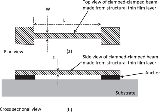
Figure 6. An illustration of a clamped beam micro-scale beam that could be used in a number of different important MEMS applications having width "W," length "L," and thickness "t."
Download figure:
Standard image High-resolution imageA typical resultant random variation of the micro-beam width made using a standard fabrication process sequence having the above dimensions likely will be at least +/− 0.50 micron. 3 In terms of relative variation, this equates to the following:
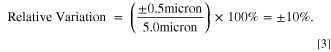
What is immediately noticeable about the relative variation of the micro-beam width is its relatively large magnitude. This example is representative of many semiconductor-based manufacturing methods.
It is useful to compare this to a more traditional macro-scale manufacturing method. An example of a commonly used method of making mechanical components at the macro-dimensional scale in a machine shop is the lathe. Assume that a cylindrical steel shaft having a nominal dimensional diameter of 100.00 millimeters is made using a lathe. A modestly capable machinist operating a lathe would be able to make the shaft with a variation of the diameter to within ±1 mil (±25.4 microns) or better. 81 The resultant relative error in this case equates to:
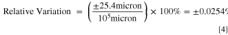
A common lathe is not the most precise machine tool available. Ultra-high-precision computer numerical control (CNC) machine tools have demonstrated dimensional variations down to a few microns or less thereby translating into a relative variation of around 0.002% for the shaft size in this example. 81
Taking the ratio of the relative variation of the shaft fabrication to that of the width of the micro-beam made using semiconductor manufacturing methods, reveals that the macroscale machining has nearly 400 times lower variation, and as much as 5,000 times lower variation for the ultra-high-precision machining tool. This example demonstrates that the relative variations of the device dimensional parameters using semiconductor manufacturing methods are significantly larger compared to those obtained using macro-scale methods.
It is worth noting that the relative variations of the dimensions made with semiconductor manufacturing methods also tend to get larger as the dimensions are reduced. Figure 7 shows the relative variations (in percentages) along the y-axis plotted against the critical feature sizes (in nm) along the x-axis for a number of manufacturing methods starting at more conventional macroscale machining techniques on the left and moving to progressively more advanced semiconductor fabrication techniques from left to right. A dotted-line is drawn approximately through the points representing these manufacturing methods showing that the relative parameter variations increase as the dimensions of the features being manufactured decrease.

Figure 7. A plot of the relative variations vs crtical minimum feature size for various methods of manufacturing. Macroscale machining is shown at the left and increasingly advanced semiconductor-based manufacturing is shown toward the right. The materials being patterned are shown for the ones using semiconductor-based manufacturing methods.
Download figure:
Standard image High-resolution imageImpact of device physics on parameter variations
The above example demonstrates that the relative variations of device parameters when using semiconductor-based manufacturing methods are comparatively large. However, this is not the whole story. The physical equations used to describe the device's output behavior often raise the values of the device dimensional parameters to higher powers. This significantly increases the impact of the parameter variations on the device output behavior. As one example, consider the volumetric fluid flow rate in a micro-channel made using semiconductor-manufacturing methods. Such a micro-channel would be common in many microfluidic devices. The Hagen-Poiseuille equation is used to describe the volumetric flow rate, Q, is given as follows: 89

where ΔP is the differential pressure across the microchannel, μ is the fluid dynamic viscosity, and L and r are the length and the radius of the microchannel, respectively. This equation assumes that the fluid is incompressible, Newtonian, and has laminar flow characteristics, which is usually applicable for microfluidic elements.
As can be observed in this relationship, any variation in the radius r of the microchannel has a magnified impact on the flow rate since this parameter is raised to the fourth power. The flow rate of the microchannel device is also proportional to one over the length of the channel, L, and this parameter may have some amount of variation as well that will also impact the flow rate. The important point that this example demonstrates is that random variations present in the device parameters of manufactured elements can have an amplified impact on the device behavior.
This is not an atypical example. Most devices with analog functionality have physical equations describing their output behavior where one or more device parameters are raised to higher powers. As another example, a pressure sensor device commonly employs a square diaphragm as the mechanical sensor element. Under uniform pressure loading, the maximum deflection, w, of a square membrane, with an edge length of 2a is at the center and is approximately given by: 90

where P is the applied uniform pressure loading and D is the flexural rigidity of the membrane given by:

In the expression above, E is the Young's modulus of the material that the diaphragm is made, t is the thickness of the diaphragm, and ν is the Poisson's ratio of the diaphragm material.
As can be seen from these equations, the deflection of the diaphragm is proportional to the diaphragm edge length to the fourth power, and inversely proportional to the thickness of the diaphragm cubed. Consequently, it would be expected that the behavior of the diaphragm would be highly dependent on the amount of variation present in both of these device dimensional parameters. Many mechanical and electromechanical functioning devices such as MEMS and NEMS, exhibit these types of device parameter-raised to higher power relationships and consequently have behavior strongly impacted by the device parameter variations resulting from the use of semiconductor-based manufacturing methods.
Combination of both bias and random manufacturing parameter variations
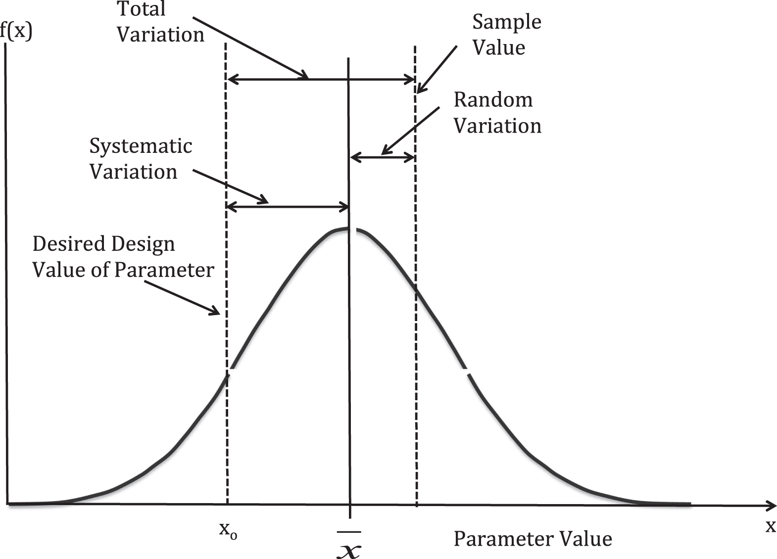
In semiconductor-based manufacturing both systematic and random device parameter variations are both present. 3 These are represented in Fig. 8 below. The normal-Gaussian-shaped curve represents the distribution of the random variations related to a parameter of the device. It is assumed that a sufficiently large number of samples have been taken of this parameter to generate this distribution. This distribution could be representative, for example, the width of a micro-beam resonator, radius of a microfluidic flow channel, or any other device parameter. Since these variations are random, they can be statistically analyzed. Further, if they are random, independent, and have equal probabilities, any sufficient number of samples of the parameter variations would be expected to exhibit a normal-Gaussian type of distribution as shown in Fig. 8. 91,92 The two defining characteristics of the normal-Gaussian distribution are the mean and the standard deviation (or variance), wherein the mean is the location of the maximum of the distribution curve and the standard deviation is representative of the amount of spread in the distribution. Therefore, if the random variations of a device parameter exhibit a large magnitude of variations, then the spread of the distribution from the mean will be larger. Due to the presence of a systematic parameter variation, the entire normal distribution will be shifted to the right or left from the "desired" design value of the device parameter by the magnitude of the systematic parameter variation.
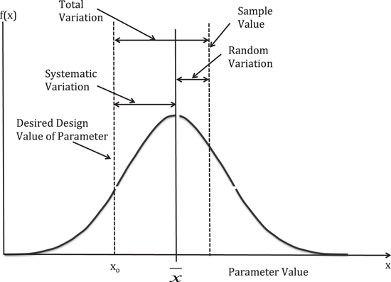
Figure 8. An illustration of the two types of variations that are typically found in manufacturing processes. The random parameter variations can usually be represented as a normal bell-shaped distribution (assuming sufficient samples are taken). The systematic parameter variations cause the resultant shift of the normal distribution from the desired value of xo. The total parameter variation for a single sample point is shown as the sum of the bias and random variations.
Download figure:
Standard image High-resolution imageEstimating Device Behavior Due to Parameter Variations
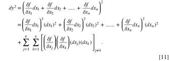
A method to estimate the variations in the output behavior of a device based on the combined random and systematic variations in the device's parameters is provided in this section. Assume there is one or more equations that describes the output behavior of a device that is a function of n independent parameters given by the variables, x1, x2, x3, ....xn, can be written as: 3,91–93

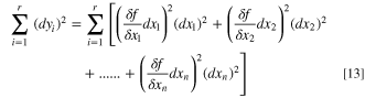
It is desired to calculate the total standard deviation of the function y = f(x1, x2, x3,....., xn )., given by σy, when the only information available is the standard deviations of each of the independent variables, x1, x2, x3, ....xn,. The equation for σy can be written as:

where μy is the mean of y, and r is the number of measurements of the population of y. Let Δy = yi—μy . Assuming Δy is small, then Δy can be approximated by: 3,91–93

Equation 9 can be rewritten as  and using Eq. 10, the following can be expressed:
3
and using Eq. 10, the following can be expressed:
3
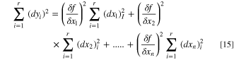
Since the variables xi are independent, then:

This same result can be shown to be true for similar terms, allowing the following to be expressed 3 :
Each of the partial derivatives can be evaluated at its respective mean value, allowing: 3

where Ci is a constant for each of the xi . Therefore, Eq. 13 can now be expressed as: 3,93
Using Eq. 15 and inserting into Eq. 9, results in the following for the variance of function y:
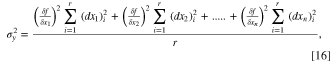
that can be re-written as:
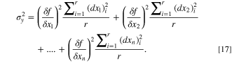
Recognizing that the  terms are variances of each of the xi
, the following can be written for the variance of function y:
3,93
terms are variances of each of the xi
, the following can be written for the variance of function y:
3,93
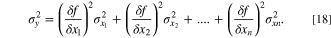
This can be re-written in terms of the standard deviation as follows: 3,93
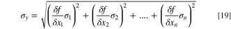
The same technique can be used to develop a similar relationship for the total amount of systematic offset in the output behavior of a device given by ey. Again, it is assumed that the output function, given by y = f(x1, x2, x3, .....,xn ), is a function of n independent variables and the total offset is due to the individual offsets in each parameter. This results in the following: 3,91,93,94
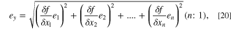
where (n:1) is the probabilities of the variables x1, x2, ...xn. Equation 19 can be used to estimate the total random parameter variation in the device output behavior when there are multiple device parameters involved, some which may be raised to higher powers. Similarly, Eq. 20 can be used to estimate the total systematic parameter variation in the equation describing the device behavior when each of the device parameters has an offset.
One remaining issue is how to combine the effects of total random and systematic device output variations to determine the total variation in the device output. If these total output variations are independent of one another then the total random and systematic variations can be combined to find the total output variation using the root sums of squares function. If the systematic and random total output variations are not independent, then they are added to estimate the total output variation. 93
Example of device output behavior variation analysis
Analysis of the total parameter variation of the microchannel will be demonstrated. The Hagen-Poiseuille equation given above relates the volumetric flow rate in the microchannel to the pressure differential, channel dimensions, and fluid properties. The Hagen-Poiseuille equation can be written in the form of a transfer function as follows:

where R is the fluidic resistance of the microchannel. The reason for expressing the Hagen-Poiseuille equation in this form is because it allows the input and output variables to be placed on one side of the equation and the device parameters (e.g., device dimensions and material property) to be placed on the other side thereby putting the relationship into a form of a transfer function that can be analyzed using the method outlined above. The estimated total normalized systematic variation in the microchannel device flow resistance can be written as:

where the individual systematic variations in the independent variables, μ, L and r are given by eμ, eL , and er , respectively. Additionally, the following can be written for the estimated total normalized standard deviation of the random variations in the microchannel device flow resistance as:

where σμ, σL , and σr are the standard deviations of the random variations of the fluid viscosity, microchannel length and microchannel radius, respectively. As can be seen in Eqs. 22 and 23, the magnitude of the estimated total systematic and random variations can be dramatically increased when the parameters are raised to higher powers, such as the microchannel radius raised to the fourth power. Each of the estimated total systematic and random variations can be combined using the root sums of squares to estimate the total output variation.
If the random parameter variation of the microchannel radius were equivalent to that of the example of the polysilicon micro-beam given above, that is +/−10%, then the impact on the flow resistance R of the device from only the microchannel radius would be +/−40%. This is a huge amount of output variation due only to this parameter alone.
The root mean of square combination of Eqs. 22 and 32 gives an estimate of the total variation of the device transfer function. However, what is needed is the interval that covers a defined proportion of the population distribution with a certain level of confidence. This is termed a tolerance interval. The issue is that the above analyses are based on the means and standard deviations of samples and not the populations. As such, there is uncertainty on the exact location of the mean due to it being determined from a sample. A tolerance interval is used to estimate the location of the manufacturing function based on the sample size. The net effect of the tolerance interval will be to increase the number of sample standard deviations used to define a region covering the proportion of the population distribution desired with a given level of confidence. The two-sided tolerance interval is calculated using the following equations: 3,91

where  is the sample mean, Sx is the sample standard deviation, and k2 is a factor that is determined so that the interval includes at least a proportion p of the population with a specified level of confidence. The k2 factors are tabularized in ISO 16269–6
95,96
and available in many references on statistics.
91
The net effect of the tolerance interval is that it increases the estimated parameter variation.
is the sample mean, Sx is the sample standard deviation, and k2 is a factor that is determined so that the interval includes at least a proportion p of the population with a specified level of confidence. The k2 factors are tabularized in ISO 16269–6
95,96
and available in many references on statistics.
91
The net effect of the tolerance interval is that it increases the estimated parameter variation.
Monte carlo variation analysis
In addition to the analytical technique reviewed above, another method called "Monte Carlo" analysis is also useful for estimating the impact of the device parameter variations on the device output variation. In fact, both methods are useful in their own way. The analytical method is extremely helpful in early semiconductor-based design and development efforts, particularly in situations where the development requires a new device design, a customized process sequence, or major changes in processing steps in the process sequence. 3 This is often the case for MEMS, microsystems, NEMS, and many kinds of non-digital IC technologies. The analytical technique allows the device designer to quickly develop reasonably good estimates of the impact of the variations on the output behavior and the yields without devoting the significant time and effort needed for a more intensive and thorough analysis using Monte Carlo. In these types of situations there are numerous complex issues involved in the design that require many changes and revisions over a number of times in order to come up with a draft device design and process sequence that appears to meet the application requirements. Performing detailed analysis using Monte Carlo at an early stage would be cumbersome and wasteful until many of the design issues were settled. Once a device design and process sequence appear to be workable using analytical methods, then Monte Carlo will enable a more detailed and accurate analysis to be performed.
The Monte Carlo method uses the device parameters described by their probability density functions and performs iterative calculations using pseudo-randomly selected values from each of the variable's probability distributions to calculate the output behavior of the device at those device parameter points. Assuming an adequate number of iterations are conducted, the result will be an accurate representation of the device output probability distribution. The measured values of the parameter variances can be used in the analysis and consequently their impact can be accurately represented in the result. Additionally, the device output is a probability distribution and it is relatively simple to determine the yield. Monte Carlo analysis can be performed on normal distributions and many other types of probability distributions with a good level of accuracy.
Figure 9 illustrates Monte Carlo. A pseudo-random number generator is used to conduct sampling from the probability distribution functions of the device parameters. The randomly selected parameters are labeled, x1i, x2i, ...xni. These device parameters combined with the device physical equations are used in the analysis. The result is a device output value that is labeled "D1i" in plot "analysis 1" in Fig. 9. This procedure of randomly choosing new device parameter values and then using the device equations to calculate the output is repeated many times. The results of these analyses can then be summed to compose a histogram of the device output. The output behavior will also be a probability distribution function with a mean indicating its most likely value and a standard deviation indicative of the amount of spread in the device output behavior. The accuracy of the calculated device output increases as the number of calculations increases in the analyses. If large numbers of iterations are performed, the histogram begins to resemble a continuous device output probability distribution function. 3,97
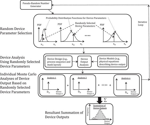
Figure 9. An illustration of the use of Monte Carlo analysis to calculate the probability distribution function of the device output.
Download figure:
Standard image High-resolution imageIt is not uncommon for devices made using semiconductor-based manufacturing methods to have correlations among some of the device parameters. Correlations can be easily included into the Monte Carlo analysis using joint probability distribution functions of the device parameters. 3,91,97
If the physical equations describing the device behavior and device parameter probability distribution functions are accurately represented in the Monte Carlo analysis, the result of a sufficient number of iterations will be an accurate representation of the actual output behavior of manufactured devices. Monte Carlo is considered an accurate representation of the results of actual manufactured devices, at a far lower cost. Monte Carlo method is also a very useful for estimation of the manufacturing yield. 3,97
Monte Carlo analysis does require that the probability distribution functions of the device parameters be known. This may not always be the case; particularly before fabrication development or manufacturing has begun. In many cases, it is possible to develop a reasonable estimate of the mean and standard deviation of the device parameters, and if these estimates are available, reasonable estimates of the probability distribution functions for the device parameters can be developed. In any case, actual measured values of the device parameter probability distribution functions should be used to replace estimates as soon as they are available. 3
Relationship Between Process Variations and Yield
The percentage of die that work and meet the requirements is called the yield. It is desired that the yield be as high as possible since this lowers the manufacturing cost. The manufacturing of most products involves the implementation of components, the assembling of sub-systems from these components, the assembling of higher-level systems from these sub-systems, and so on, eventually resulting in completed products. During production, some amount of the components, sub-systems, and systems will be rejected for not meeting the requirements. Nevertheless, the production methods employed enable any defective items to be detected before assembly, and replaced so that they do not lower the yield of sub-systems or systems in later stages of manufacturing. These manufacturing practices are very common in production of most assembled products including cars, cell phones, appliances, tools, etc.
Semiconductor-based manufacturing is unique compared to these familiar modes of production. It involves performing a series of processing steps on substrates. The processing steps often involve chemical, electro-chemical, plasma, thermal, etc., treatments where the effects of these treatments on the substrates are not reversible. If a processing step has a poor result, the entire batch of substrates, as well as all of the fabrication work up to that point in the process sequence can be lost. Die that do not work or do not meet the requirements cannot be re-worked. Additionally, non-working die on the substrate cannot be swapped out and replaced during manufacturing. Non-functional die remain on the substrates to the end of the manufacturing and thereby represent a wasted cost.
There are two general types of yield of interest. The first is functional yield, which is the percentage of the manufactured die that are operational. Functional yield models are usually based on defects, commonly called "killer defects" that render the die inoperable. There are a number of models developed mostly by the IC industry for estimating functional yields. 98–101 The second is parametric yield, which is the percentage of functional die that meets specific pre-defined application requirements. Parametric yield is more important since it provides the metric of die that can be used in the intended application and is more relevant to the discussion of device parameter variations. 3,97
As explained above, the random variations exhibited in the device parameters, such as the dimensions and material properties, can be represented by probability distribution functions. Further, the systematic offset in the parameters can be represented by a shift of the probability distribution functions. The device output can also be represented by a probability distribution function derived from the probability distribution functions of the parameters and the transfer function defining the relationship between the device input and output, and the device parameters. The systematic variation in the device output is represented by the shift in the output probability distribution function. The probability distribution function of the device output is also commonly called the manufacturing function. The manufacturing function can be used to estimate the parametric yield. 3
The device output can usually be represented by a normal distribution function. In one dimension, represented by the variable x, this would be written as follows: 3,91,92,97

where μ is the mean and σ is the standard deviation of the population.
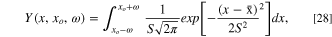
The probability of a specific value of some device output is represented by integrating over the area from x1 to x2 as follows: 92

An adequate sample size (e.g., more than 30 samples) of the individual measurements of the variations of the population of device output can be represented by a normal distribution having a mean value,  and standard deviation, S.
The mean value provides information about the location (along a defined parameter axis) of the maximum probability of the device output and the standard deviation provides information on how much spread there is in the device output sample data. An example of the probability distribution function of a device output is shown in Fig. 10. The number of standard deviations on each side of the mean is shown wherein about 68.2% of the population resides within one standard deviation, 95.4% of the population resides within two standard deviations, and 99.7% of the population resides within three standard deviations. The mean of the manufacturing function is 
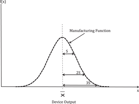
Figure 10. An illustration of a device manufacturing function.
Download figure:
Standard image High-resolution imageThere is usually a range of output values where the device performs adequately to meet or exceed the performance requirements for the intended application. This is usually called the acceptance range and can be represented by the function, Af(x), having a value of 1 when x is between the two limits given by xo ± ω of a mid-point of the range, xo, and 0 outside of this range as shown in Fig. 11. The acceptance range is expressed as: 3

It is usually desired that the value of xo is equal to the mean value of the manufacturing function so as to align the centers of the manufacturing function and acceptance range.

Figure 11. The acceptance range.
Download figure:
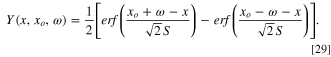
Standard image High-resolution imageUsing the manufacturing function from above, where the sample mean,  and standard deviation, S, are substituted for the population mean, μ, and standard deviation, σ, and combining with Eqs. 25 and 26 allows the expression for the parametric yield to be written as:
3
and standard deviation, S, are substituted for the population mean, μ, and standard deviation, σ, and combining with Eqs. 25 and 26 allows the expression for the parametric yield to be written as:
3
that can be re-expressed as follows: 3
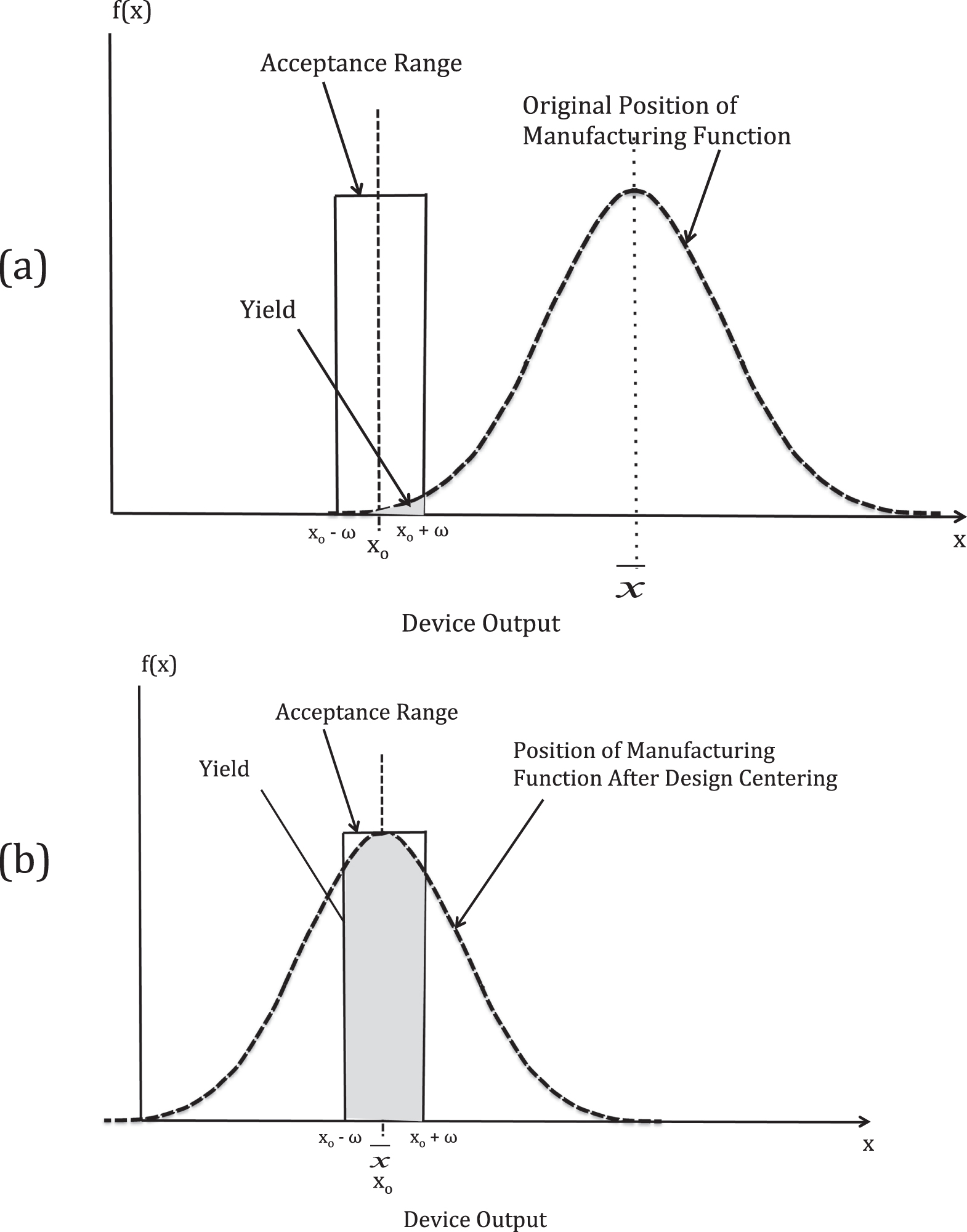
The overlay of the manufacturing function and acceptance range is shown in Fig. 12. The yield is given by the number die included within the overlap of the manufacturing function and the acceptance range (shown as shaded region in Fig. 12). 3 Since the acceptance range only covers less than half of the entire manufacturing function, the yield will be below 50%. This would be considered a low value of yield.
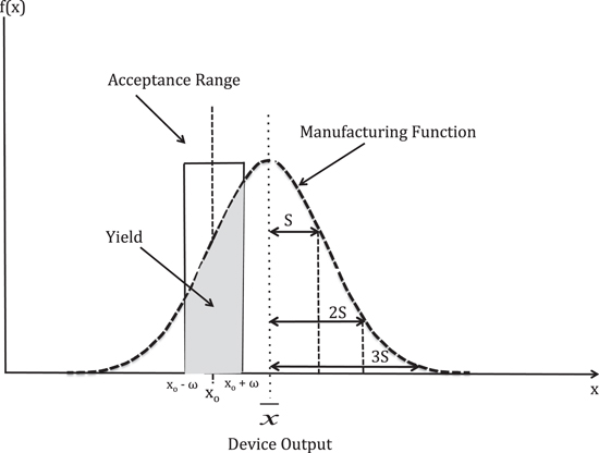
Figure 12. Overlay of the manufacturing function and the acceptance range for the device output behavior. The yield is the overlap of these two functions.
Download figure:
Standard image High-resolution imageThere are two reasons that the yield is low. The first is that the acceptable range is shifted from the center of the manufacturing function. This is due to a systematic offset in the output of the device due to one or more systematic offsets in the device parameters. The second is that the manufacturing function has a spread that far exceeds the width of the acceptance range. Recall that the amount of spread in the manufacturing function is indicative of large random variations in the device parameters. Even if the acceptance range were perfectly aligned with the center of the manufacturing function by elimination of the systematic offsets, the yield would still be below 50% due to the amount of spread in the manufacturing function.
In most practical scenarios, the device parameter space will have a multiplicity of parameters. In such cases, the parameter space can be represented by a dimensional space equivalent to the number of device parameters. Likewise, the output parameter space may also be multidimensional. If the performance parameter space is multi-dimensional, the yield can be written as follows:

where Ω(x1, x2, ....., xn ) is the n-dimensional Gaussian probability distribution manufacturing function and the integration limits are the boundaries of the acceptance ranges for each of the parameters.
While the acceptance range boundaries are known in the device output parameter space, this is not true for the device parameter space. The device output appplication requirements must be transformed into boundaries within the input parameter space in order to determine the relationship between the acceptance region and the parameter variation limits. This can be difficult when the device output is dependent on a number of different device parameters. In general, computer algorithms are often used to determine the boundaries of the acceptance range in the device parameter space. 3
Monte Carlo yield estimation
Monte Carlo can be used for estimating the manufacturing yield. 3,97 The probability distribution functions of the device parameters are used for pseudo-randomly selecting samples for the analysis of the output behavior of the device. With each of the pseudo-randomly selected samples the output behavior of the device is evaluated using the physical equations describing the device. The output behavior is described by a manufacturing function that is a probability distribution function. Depending on the values of the device outputs, the device at each sample point is declared as either a "pass" or "fail" depending on whether it meets or does not meet the device output application requirements set by the acceptance range. The yield is estimated by counting the number of passing points, given by N, divided by the total number of samples, N, or:

An important item to note with using Monte Carlo methods to estimate the yield is that the location and boundaries of the acceptance range is not required.
An advantage of Monte Carlo analysis is that it enables an accurate yield estimate to be calculated. Assuming a sufficient number of Monte Carlo analyses are performed (i.e., usually more than 30), the central-limit theorem asserts that probability distribution function of the yield will have a normal distribution thereby allowing the following to be expressed: 3,92

where  is the z-variable for the normal distribution,
  is the distribution of the sample mean of yields derived from averaging random samples of size n drawn (with replacement), μ is the mean, σ is the standard deviation, and n is the number of samples. If there are multiple random samples of the yield, given by Y1, Y2,....Yn that have a mean m and standard deviation σ, if n is sufficiently large, then
  has a normal distribution with a mean given by μ and a standard deviation given by
  The relationship for μ can be expressed in terms of the confidence interval for μ with a confidence level of 100(1 − α)% as:
3,91,92
The relationship for μ can be expressed in terms of the confidence interval for μ with a confidence level of 100(1 − α)% as:
3,91,92

 and σ are commonly estimated with a yield sample mean YAverage and a yield sample standard deviation s, respectively, thereby allowing the following to be written for the confidence interval:

If the number of samples is small (i.e., less than 30) with a normal distribution, the confidence interval for the yield mean can be estimated using the t-distribution resulting in the following for the confidence interval for μ with a confidence level of 100(1 − α)%: 3,91,92

In cases where it is not known if the distribution is normal, the distribution should be tested for normalcy.
The number of iterations of Monte Carlo analysis, given by n, required to obtain a desired confidence interval given by 100(1 − α) can be written as: 3,91

and solving for n.
Managing Device Parameter Variations in Device Design
The methods used in device design implemented using semiconductor-based manufacturing includes the following: 3
- (1)Design centering . Design centering adjusts the nominal values of one or more device parameters so that the middle of the manufacturing function and the acceptance range align. Design centering often consists of adjusting the nominal values by removing systematic offsets in the device parameter values. This is usually the easiest and most cost-effective method to increase the yield. It is almost always performed before any of the other methods are attempted.
- (2)Reduction of random parameter variation . This method focuses on reduction of the amount of random variation in one or more device parameters. This is done by decreasing the standard deviations (or variances) of the device parameters. Reducing the random variation can be difficult using standardized semiconductor-based manufacturing equipment, and therefore, this method usually involves employing different processing steps or tool technologies that have lower random variations. This method often results in an increase in the manufacturing cost.
- (3)Device size scaling . This method is aimed at reducing the amount of relative variation in one or more parameters. Many of the random variations in lateral dimensions of devices are not percentages of the dimension of a critical feature, but instead have a fixed or constant value. As noted above, the random variations of features using contact photolithography are commonly expressed as ±0.5 microns. Therefore, if the overall dimensions of the device critical features are increased, it will result in a reduction of the relative variations. Note that since the device features are made larger and, therefore, consume more substrate area, this results in increased die costs.
- (4)Acceptance range increase . This method enlarges the acceptance range boundaries of the acceptable device output. In most circumstances, this will not be a desirable choice since it lowers the performance of the device.
- (5)Best practices on mask layout design . The mask layout of devices has an impact on how sensitive the design is to manufacturing variations and, therefore, there are several methods that can be used to reduce this sensitivity. These include: matching; minimizing orientation effects; symmetry; inter-digitation; common centroid; and others. 3
Each of these is explained in further detail below.
Design centering
Design centering is achieved by adjusting the nominal values of one or more device parameters in order to shift the manufacturing function so that its center aligns with the mid-point of the acceptance range. 3 In short, this effectively removes the systematic (offset) variations in the device parameter(s). These systematic variations are the result of the processing steps used to manufacture the device. For example, systematic variation can be caused in photolithography by a small amount of difference from the as-drawn mask dimensions and the features made in the photoresist that can result from over- or under-exposure of the photoresist. Likewise, there may be a small difference in the dimensions of the design and the etched features due to some small amount of lateral etching, since no etch process is perfectly anisotropic. These variations are usually not difficult or expensive to remove, and most often can be addressed by a biasing of the mask dimensions to account for the offset.
Figure 13 illustrates design centering. In Fig. 13a, the manufacturing function for the device output is shown with the acceptance range. Due to a significantly amount of systematic variation, there is an offset between the center value of the manufacturing function and the acceptance range. Consequently, the yield for Fig. 13a given by the overlap of these two functions is very low.
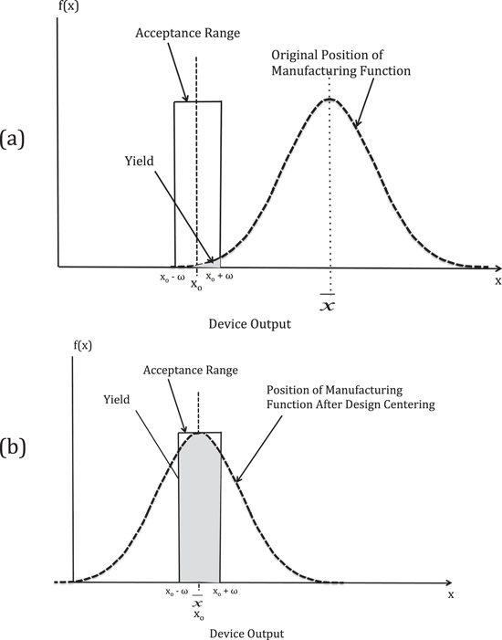
Figure 13. Illustration of design centering wherein the manufacturing function is shifted from an original position (shown in (a)) to a new position (shown in (b)) after the systematic variations have been removed. In the new location, the center of the manufacturing function and acceptance range align.
Download figure:
Standard image High-resolution imageIn Fig. 13b is shown after the manufacturing function after having undergone design centering. As a result of this procedure, the manufacturing function is shifted towards the left such that its mid-point, given by  aligns with the mid-point of the acceptance range, given by xo. The yield of the manufacturing process given by the overlap of the two functions has been significantly improved. Having said that, the resultant yield is still below 50% due to the large amount of random variation in the device output behavior, and this is caused by the large amount of random variation in the device parameters.
It should be noted that it is implied in the discussion of design centering that the device critical features can be inspected and measured during and after manufacturing. This is usually the case. However, in some situations it may be difficult to measure the critical features. In those cases, methods to indirectly measure these critical features may be needed. Additionally, adjusting the nominal value of device parameters could also affect the manufacturing function. Therefore, it is advisable to re-perform the device analysis based on the biasing changes made.
Device parameter random variation reduction
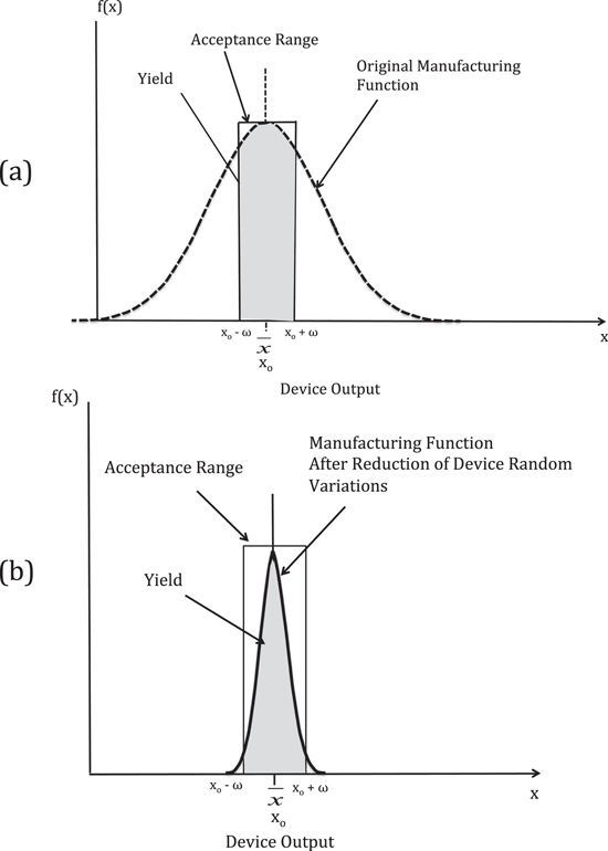
As shown in Fig. 13, even after performing design centering the manufacturing function may extend well beyond the acceptance range, thereby resulting in an improved, but still low yield. If the standard deviation in the manufacturing function of the device can be sufficiently reduced this would significantly improve the yield. 3
For example, the polysilicon micro-beam resonator in the example above had a specified random variation of 5.0 ± 0.5 microns in the width using contact lithography and standard reactive ion etching (RIE). If the contact lithography were replaced with the use of a deep-ultra-violet (Deep UV) exposure tool, and the standard reactive ion etch were replaced with a more anisotropic inductively-coupled plasma (ICP) etch, the random variation in the width of the beam could be reduced to 5.0 ± 0.1 microns resulting in a 5X reduction in the magnitude of the random variation of the width. The device physics will also play a role in the total output variation due to the device parameter variations. However, if we assume the width is the only important device parameter and it is raised to only the first power in the device transfer function, then we would expect the manufacturing standard deviation to decrease also by a factor of five. The result is shown in Fig. 14. It should be noted that the design centering from above was retained, and therefore, Fig. 14 shows the result of design centering and device parameter random variation reduction.
Figure 14. The manufacturing function using more advanced semiconductor-based processing steps that decrease the random variations in the device parameter from their original values (shown in (a)) to the new values (shown in (b)), thereby also resulting in a decrease in the standard deviation of the manufacturing function. The manufacturing function has also been design centered.
Download figure:
Standard image High-resolution image
As can be seen in Fig. 14, reduction of the random variation in the polysilicon micro-beam resonator width significantly reduced the standard deviation of the manufacturing function such that the entre function is almost completely enclosed by the acceptance range. This will result in an improved yeild. Therefore, the reduction of the random variations of the device parameter (combined with design centering) resulted in a significantly improved yield. Neverthelsss, it is important to point out that the Deep UV lithography and ICP etch are considerably more expensive than contact photolithography and standard RIE. Therefore, the device designer must always evaluate if the improved yield compensates for the increased manufacturing cost.
Device size scaling
The scaling of the device size is another method to reduce random device parameter variations. The concept of device size scaling is that many semiconductor-based manufacturing methods have variations that are fixed, regardless of the absolute value of the feature. 3
An example of this is the polysilicon micro-beam examined above wherein if contact photolithography and standard RIE are used to implement this structure there will be a variation of ±0.5 micron no matter the size of the feature. As seen above, if the width of the micro-beam is 5.0 microns, the variation in the feature results in a ±10% relative variation. However, if the dimension of the width is increased, say to 50.0 microns, the relative random variation will drop to ± 1%. Therefore, the standard deviation of the manufacturing function will be reduced by a factor of ten, assuming that the width dimension is the only device parameter of importance, and the width is only raised to the first power in the device physical behvior equation. Therefore, increasing the width by a factor of ten will result in a ten-fold reduction of the spread of the manufacturing function compared to the orginial manufacturing function.
Device size scaling can be used to increase the yields using semiconductor-based manufacturing methods. However, it should be noted that the cost of device size scaling is the consumption of additional substrate area. Consequently, the device designer must weigh the yield improvement gained by device size scaling against the increased cost of the die. The designer will also need to consider any effects to the device operation based on the size scaling.
An issue of device size scaling is that it is only useful if the random parameter variations are absolute in magnitude. Consequently, this technique will not be appropriate for reducing the random variations in the thicknesses of deposited thin-film layers. Since the random variations in these layers is a percentage of the thin-film thickness, increasing the thickness of the layer does not result in a reduction in the amount of random variation.
Acceptance range increase
The acceptance range is ususally determined by the application requirements, and, therefore, increasing it is usually not an acceptable avenue to increase the yield. Nevertheless, it is important to point out that the designer can examine the acceptance ranges of individual device parameters. Often the acceptance ranges of individual parameters can be individually adjusted so as to obtain a higher overall yield. In these situations, some of the individual parameters can be made more or less restrictive in order to result in a higher overall manufacturing yield. Therefore, the device designer must carefully examine each of the device parameters involved in the output behavior and understand their relative impact on the manufacturing yield. 3
As an example, consider a silicon pressure sensor that employs a square-shaped diaphragm as the mechanically compliant sensing element. Under an applied uniform pressure loading the maximum deflection, w, of a square membrane with an edge length of 2a is at the center and is approximately given by: 90

where P is the applied uniform pressure loading, E is the Young's modulus of the material from which the diaphragm is made, t is the thickness of the membrane, and ν is the Poisson's ratio of the membrane material. The two important dimensional parameters in Eq. 37 are the edge length of the membrane, a, which is raised to the fourth power and the thickness, t, which is raised to the third power.
In semiconductor-based manufacturing, the thickness of the membrane will likely have the largest contribution to the total random variation of the output of the pressure sensor and, as noted above, the designer may not have any options on reducing the variation in this parameter. Nevertheless, the device designer can focus on reducing the random variation in the membrane edge length, perhaps sufficiently to compensate for any unavoidable random variation of the membrane thickness.
Best practices in layout design
The layout design of devices is important to ensure devices are not sensitive to the effects of random parameter variations. The matching of components is a commonly employed method. Matching refers to components or features that are specified to have identical values or values that are multiples of one another. Perhaps the most common example of a matched component design is the switched capacitor circuit. 102 The response of this configuration depends on the ratio of the capacitors and not their absolute values. The ratios of components, such as capacitors, are much more accurately defined using semiconductor-based manufacturing methods compared to the absolute values, due to the presence of correlated random parameter variations. Matching can be done with many different types of passive and active components. It is best to position matching elements close to one another. 3
The orientation of the design of components and features is also important. This is because it is common in semiconductor-based manufacturing methods for the resultant random variations in the dimensions to be dependent on the orientation of the substrate. Therefore, for components and features that are to have consistent parameter values, it is best to orient the features in the same direction on the substrate.
It is useful to attempt to layout the devices in the design so that the geometrical shapes are matched. Devices made with rectangular features should not be combined with circular features, if possible.
Additionally, when there are devices having large areas involved in a design, it can be advantageous to segment the devices into parts, and interweave these parts in order to better cancel out any device parameter random variations.
When attempting to match a number of components or features in their parameter values, it is prudent to use a middle value of the component or feature as the root value rather than the lowest common value.
Inter-digitation of the components or features is helpful in some design situations since it will allow the components and devices to be located in closer proximity to one another, thereby resulting in less sensitivity to parameter random variations.
Common centroid design techniques are designs where the elements or features are located around a common center. The result is that random parameter variations affect the components more or less equally.
It is always a good practice to use symmetry in the design of components and features. Asymmetric designs by definition create imbalances that can make the device more sensitive to parameter random variations.
It is advisable to use dummy devices in the design of devices and features in order to cancel out any end effects that result from the manufacturing methods. This is especially useful for etching arrays of features where the end features may have a different etch rate than those in the center.
Design features that are to be implemented using etching should attempt to make the width dimension of the etched features equivalent across the design. This is because features having larger widths etch faster than narrow features and therefore, over-etching will be needed in order to complete the etch on all of the features.
Signal conduction paths in the design should be kept as short as possible, and if there are parallel signal conduction paths, they should have the same length, geometry and orientation.
Material Property Variations
The discussion to present has mostly focused on the impact of dimensional device parameter variations. As noted above, the material properties are also often a variable component in the transfer functions of devices, such as the viscosity of fluids in the microchannel or Young's modulus of the mechanically compliant membrane in the pressure sensor. Semiconductor-based manufacturing has another unique characteristic compared to most all other manufacturing domains in that the material properties often depend on the processing steps used. Thin-film deposited material layers often exhibit material properties that strongly depend on the processing step recipe. 3,84,85,97,103 Therefore, it is not uncommon to find thin-film material layers with vastly different material property values for common processing steps such as chemical-vapor deposition, physical-vapor deposition, and others. Additionally, the values of the material properties can significantly change after subsequent processing steps are performed. 3 The residual stress value of a deposited layer after deposition can change drastically if the layer is exposed to a subsequent thermal process. 3 Therefore, the device designer must be prepared to perform measurements of the properties of materials used in the device design based on the processing step used and the process sequence for manufacturing the device.
It is very common that the property of a material is not equivalent to the design value of that property. In many situations, performing extensive processing step recipe development work to adjust the value of the material property is very time consuming and expensive with at best an uncertain outcome. 3 In most cases, it will be best to accept the value of the material property as it is, and make changes in the dimensions of the device parameter to compensate for the difference in the material property value from the desired ideal value.
Conclusions
This review paper has discussed the issue of device parameter variations in devices implemented using semiconductor-based manufacturing methods. This topic is important to devices and systems implemented using semiconductor-based manufacturing, namely micro- and nano-devices and –systems. It is especially important for any non-digital IC technologies, such as analog circuits, microsensors, MEMS, NEMS, photonics, and others, as well as nanometer scale digital devices. A comparison of the relative variations in the dimensions of features made using semiconductor-based manufacturing methods was compared to macro-scale machining, wherein it was shown that micro- and nano-fabrication methods usually have relatively large relative variations compared to conventional machining operations. Additionally, it was shown that the physics describing the device behavior, particularly those with analog functionality, often raises one or more of the device parameters to higher powers, and thereby amplifies the effects of the large relative variations even more on the device output. Methods to estimate the effects of both systematic and random variation device parameter variations on the device output behavior were explained, as well as methods to combine these two sources of variation into a total estimated output variation. The impact of these variations on the manufacturing yield was explained. Finally, methods available to device designers to manage the device parameter variations were provided.
While the methods outlines in this paper for handling process variations are applicable to any type of device or system made using semiconductor manufacturing methods, most of the software tools are standalone or ad hoc. That is, there are no existing fully integrated modeling and simulation tools available that perform all of the needed functions outlined here. A more challenging issue is the estimation of the device parameter variations for a customized process sequence. As noted above, an estimate can be generated by a highly experienced fabricator, but software tools for doing this are not yet available.