
Abstract
Nanoporous anodized tin oxide films have many potential applications in the fields of photocatalysis, sensors and electrode materials. In this paper, we found that potential played a dominant role in the morphological evolution of anodized tin oxide films in electrolyte containing F− and S2−. The critical potential for the formation of nanoporous structure was determined. Porous anodized tin oxide films with different nanostructure can be prepared by the application of low anodization potential and high anodization potential. The I–V curve analysis showed that the change of the nanoporous of tin oxide films at different potentials could be attributed to the oxygen which generated by the electronic current. The valence regulation of Sn element in anodized tin oxide film can be achieved by controlling the potential.
Export citation and abstract BibTeX RIS

This is an open access article distributed under the terms of the Creative Commons Attribution 4.0 License (CC BY, http://creativecommons.org/licenses/by/4.0/), which permits unrestricted reuse of the work in any medium, provided the original work is properly cited.
Over the past two decades, nanostructure tin oxide due to its unique optical and electrical properties has been widely used as catalysts, solid gas sensors, electrode materials, photovoltaic devices and so on.1–4 Meanwhile, several techniques which could prepare nanostructure tin oxide have been developed, including thermal template-assisted methods,5 electrospinning,6 solution-based synthesis,7 evaporation,8 anodization.9–15 In this regard, the electrochemical anodization has attracted great interest due to its extreme simplicity and low cost.
For metal tin, a simple one-step anodization was performed in acidic electrolytes,9–11 alkaline electrolytes,10–13 and organic electrolytes containing F− and S.2–15 An irregular and randomly distributed porous tin oxide layer is obtained, which is completely different from the hexagonal array of porous anodized aluminum oxide16 or nanotube titanium oxide.17–19 The formed oxide layer is amorphous and can be converted into crystalline SnO2 and SnO by annealing treatment. These crystals may be advantageous to its application for photocatalysis due to the self-doping effect of multivalent tin oxide.14,20–22
It should be mentioned that the morphology of nanoporous anodized tin oxide films have a great impact on further potential applications. For example, when nanoporous tin oxide films is applied in gas-sensing devices, its property entirely depends on whether they have well-defined open porous structures.9 In addition, the transverse cracks generated during tin anodization greatly reduce the mechanical stability of the tin oxide film and increase the total resistance of the oxide layer.15,23
It is generally believed that the morphology of anodized metal oxide films (e.g. Al,16 Ti,17 Fe,24 etc.) is regulated by the process parameters during anodization. However, in earlier studies, researchers12,25 believed that the morphology of nanoporous tin oxide films was less affected by the process parameters of anodization when an electrolyte system was determined. Only the thickness of the oxide film was changed when the electrolyte concentration, potential (including 5–15 V) and time of anodization were changed. The pore size and wall thickness of nanoporous tin oxide films were not affected by these parameters. Subsequently, a systematic study by Zaraska et al.9,23,26 found that the anodized tin oxide films consisted of the inner and outer layers. The pore size of the inner layer was independent of the parameters, while the pore size of the outer layer was varied with the parameters. It must be mentioned that the outer layer of tin oxide film was relatively thin. Prolonged anodization lead to the disappearance of the outer layer, which may be the reason why researchers believed that the morphology of nanoporous tin oxide films was not independent of process parameters in earlier studies.
Among the numerous parameters of anodization, the morphology of nanoporous tin oxide films is probably most affected by the potential, because the morphology of the anodized tin oxide films can be greatly changed at relatively low potential in different electrolyte systems. In the oxalic acid electrolyte, tin oxide with nanoporous structure could be existed only when the potential of anodization was higher than 3 V, otherwise tin oxalate particles were formed on the surface of tin anode.9 In the sodium hydroxide electrolyte, a tin oxide film with the pore size of about 10 nm was obtained at 2 V. After using a higher potential, the pore size of the inner layer of the porous oxide films remained around 42 nm and was independent of the anodization conditions.26 In addition, the transverse cracks were generated in tin oxide films and increased with the potential. Zaraska et al.26 obtained crack-free oxide films by low potential anodization in sodium hydroxide electrolyte, indicating that there was a certain critical potential for crack formation.
However, the research on the anodization of tin mainly focused on the electrolyte systems of oxalic acid and sodium hydroxide. The study of anodization of Sn in other electrolyte systems (e.g. organic electrolytes containing F− and S2−) has generally focused more on practical applications, such as photocatalytic and gas-sensitive properties.14,15 However, the critical potential for the formation of nanoporous anodized tin oxide films is not yet clear in containing F−and S2−. Furthermore, the mechanism of the effect of the potential (especially the relatively low potential) on the nanostructure formation of tin oxide films during the corresponding anodization process.
In this work, we have characterized and analyzed the morphology, crystal structure and valence state of the anodized tin films obtained by adjusting the potential in electrolytes containing F− and S2−. The results indicated that the morphology and valence state of the anodized tin film were affected by the potential. And the formation and morphological changes of potential-controlled nanoporous structures were closely related to oxygen. To the best of our knowledge, the effect of potential on the morphology and electrochemical behavior of anodized tin oxide films has not been systematically studied in the current electrolyte system. It should be emphasized that potentiodynamic anodization may contribute to the determination of the critical potential for the formation of nanoporous tin oxide layers in the electrolyte where porous tin oxide can be obtained (such as NH3). In particular, the combination of electrolyte erosion and oxygen overflow resulted in the anodized tin oxide films with a tunable pore size that could be obtained at 3 V, and the thickness of the tin oxide film was not affected by time.
Experimental
The Sn foil (99.9%) was cut into specimens with the dimensions of 1.5 cm × 2 cm and cleaned by immersing in ethanol and acetone. The samples were sealed by insulating glue and the active area which was exposed to the electrolyte solution was 1.5 cm2. All experiments were carried out in a two-electrode cell, with the Sn specimen serving as the anode and graphite as the cathode. Programmable DC power supply (SOYI-1502DM) was employed during the anodization experiments. The potentiodynamically sweep rate was 0.1 V s−1 and the applied potentiostatic were 2–6 V and 8 V. The time of potentiostatic anodization was 10 min and 5 min for 2–6 V and 8 V, respectively. The experimental temperature was maintained at 25 °C. The electrolyte solution consists of ethylene glycol and deionized water (40:60 volume ratio), which contains 0.2 M Na2S·xH2O and 0.1 M NH4F. After anodization, samples were rinsed several times with ethanol and deionized water, and dried. The morphology of the anodized tin film was investigated using a field emission scanning electron microscope (FE-SEM Zeiss-Supra 55). The average pore diameter of the porous structures was determined by analyzing the SEM micrographs using Image-Pro Plus software. The crystalline structure was analyzed by X-ray diffraction (XRD)-Empyrean (PANalytical B.V. Netherlands) with Cu Kα and analyzed by JADE software. Raman scattering analysis was carried out in DXR Raman microscope (Thermo Fisher Scientific, the U.S.) using the backscattering configuration and the 532 nm line of a solid-state laser acted as the excitation source. X-ray photoelectron spectroscopy (XPS) was conducted with a Thermo fisher ESCALAB250Xi XPS system with a monochromatic X-ray source (Al-Kα line of 1486.6 eV, 15 kV, 10 mA, 150 W).
Results and Discussion
Potentiodynamic polarization curve (I–V curve) and I–T curve
Potentiodynamic anodization at a constant potential rate of change (0.1 V s−1) was carried out to analyze the electrochemical reactions that might occur on the surface of Sn anode in the electrolyte containing F− and S2−. As shown in Fig. 1a, a linear polarization curve was recorded in the potential range from 0 to 8 V. Up to 2.4 V, a relatively low current was observed. And the current was continuously increased with potential. It is assumed that the anodized oxide film with conductivity mainly depends on the migration of metal cations and oxygen anions to produce uniform thickness.27 Then the growth of barrier oxide film can be described by Eq. 1.

where U is the applied potential, t is the anodizing time, E is the electric field across the oxide, and h is the thickness of anodized oxide film. Considering Faraday's law, the following equation can be described by Eq. 2.

where ƞ is the current efficiency for film growth, Mv is the molar volume, j is the anodizing current density, z is the equivalent number, and F is Faraday's constant. Eq. 2 indicates that the current density should have a constant value during potentiodynamic anodization. However, the current density was gradually increased when the potential was higher than 2.4 V in Fig. 1a, the Eq. 2 at this time can be described as


Figure 1. (a) Linear polarization curve recorded by a Sn electrode at a potential scanning rate of 0.1 V s−1; (b) Typical current density vs time recorded during Sn anodization at different potentials.
Download figure:
Standard image High-resolution imageIt is shown that there must be other currents to increase the total current density j in addition to the ionic currents passing through the oxide layer during the potentiodynamic anodization. In fact, the large amount of gas generated on the surface of the anode indicated that the proportion of the electronic current to the total current was quite high. Therefore, two main anode reactions are considered in this system: anodization of Sn (1a) and formation of gaseous oxygen (2a).9
Because the anode potential for reaction (1a) is significantly lower than the anode potential of reaction (2a), the anode metal will dissolve before releasing oxygen. It is indicated that tin oxide was first formed on the surface of the tin anode. As the anodization potential became higher, the oxygen at the anode was released and gradually stronger. According to literature reports,28–30 oxygen generated by electronic current play a crucial role for the formation of porous nanostructure. Therefore, for the linear polarization curve shown in Fig. 1a, there was no significant change in the current density below 2.4 V, suggesting a passive nature of the film produced on the surface of Sn electrode. However, when the potential was higher than 2.4 V, the continuous increase of current density might indicated breakdown of the passivation layer and formation of nanoporous. In other words, the critical potential for the formation of porous tin oxide films under the current electrolyte system may be 2.4 V. In fact, this result is consistent with the latter potentiostatic anodization.
Based on the results of potentiodynamically anodization, we performed constant potential anodization in the range of 2–6 V and 8 V. The current density vs time curve in the potential range of 3–6 V was recorded in Fig. 1b. Three classical stages were observed: (1) stage 1 where the current density rapidly decreases, indicating the rapid formation of dense anodized tin oxide film; (2) stage 2 where the current density slowly increases with time, indicating that the gradual formation of anodized tin oxides with the porous morphology; (3) stage 3 where the current density was in a steady-state when the anodization oxidation time were further extended, indicating that the anodized tin oxide film has entered the steady-state growth stage of the porous nanochannel. It is worth noting that the current density transition curve obtained at 6 V in Fig. 1b was gradually decreased after 400 s. It might be related to the dramatic release of oxygen at 6 V, which affected the transport of ions in the electrolyte near the anode.
Constant potential anodization at 2 V and 3 V
Figures 2a–2c shows the top view of tin oxide film obtained after different time of anodization at 2 V. As can be seen, even if the tin substrate was anodized for 60 min, no nanoporous structure were appeared on the anode (shown in Fig. 2c). In contrast, with the increase of the time of anodization, the noticeable dense oxide were found on the anodized samples. It is noteworthy that the potential at this point (2 V) is lower than that at which oxygen is produced (2.4 V). It is indicated that a lack of oxygen during the growth of tin oxide as a mold to obtain nanoporous structures.28
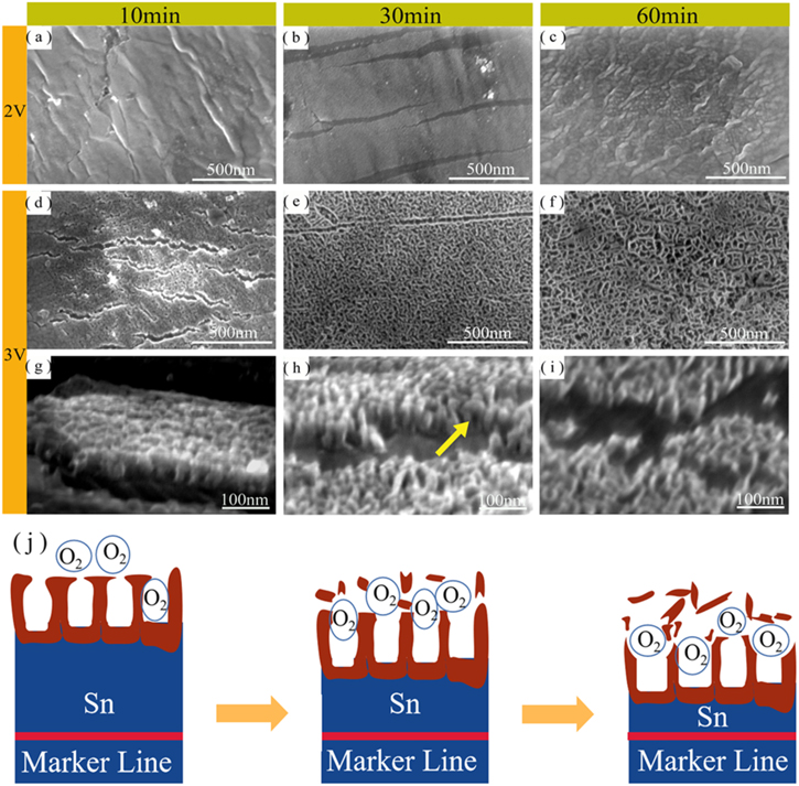
Figure 2. FE-SEM images of 2 V (a)–(c) and 3 V (d)–(i) anodized in electrolyte containing F− and S2− at different times.(a)–(f)are the top views and (g)–(i) are the cross sectional views. (j) a schematic diagram for explaining the relationship between the morphology of the anodized tin film and the oxidation time at 3 V.
Download figure:
Standard image High-resolution imageThe top and cross-section view of the tin oxide film after anodizing for different times at 3 V are shown in Figs. 2d–2i. As can be seen, the anodized tin oxide films on the surface of anode had nanoporous structure. When the potential of anodization was more than 2.4 V, the oxygen bubbles generated can be used as a mold to transform the growth behavior of tin oxide film from compact to porous.28 The yellow arrow in Fig. 2h suggests that the cavity surrounded by oxides may be caused by the oxygen mold.
Figure 3 shows the variation of pore size and tin oxide layer thickness of anodized tin oxide films with time at 3 V. With the extension of the oxidation time, the average pore diameter of the surface was increased from about 10 nm to about 23 nm. Meanwhile, the thickness of the tin oxide layer was maintained in the range of 54–60 nm. The schematic diagram in Fig. 2j is used to explain the morphology evolution of anodized tin film at 3 V. On the one hand, the pore size of the nanoporous tin oxide film was increased due to the continuous destruction of the surface of the porous tin oxide film by corrosive electrolytes and overflowing oxygen bubbles. On the other hand, the limited ionic current (for the generation of oxides) and the erosion environment of electrolytes at 3 V lead to the slower growth of porous anodized tin oxide film, which seriously hinders the increase of oxide film thickness.

Figure 3. Variation of pore diameter and oxide film thickness with time at 3 V.
Download figure:
Standard image High-resolution imageConstant potential anodization at 4–6 V
Figure 4 shows the top and the cross-sectional view of the tin oxide films obtained after anodization for 10 min in a range of 4–6 V. It can be seen that the obtained nanoporous anodized tin oxide films were disordered and randomly distributed. Meanwhile, the average oxide growth rate was increased exponentially from the potential (see Fig. 5a), which was consistent with the results obtained by Zaraska et al.26 in NaOH solution.
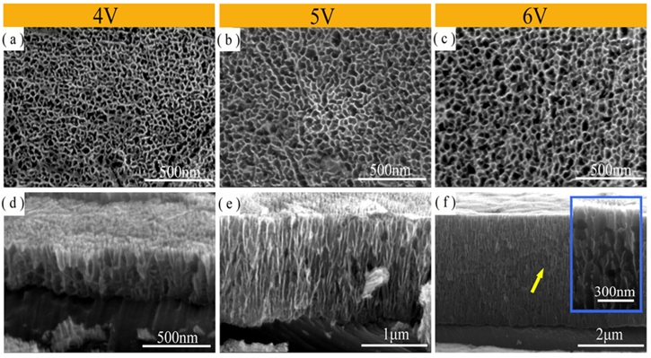
Figure 4. Top views (a)–(c) and cross-sectional views (d)–(f) of anodized tin oxide films on Sn substrates at different potentials, the illustration in (f) is a cross-sectional view at higher multiples.
Download figure:
Standard image High-resolution image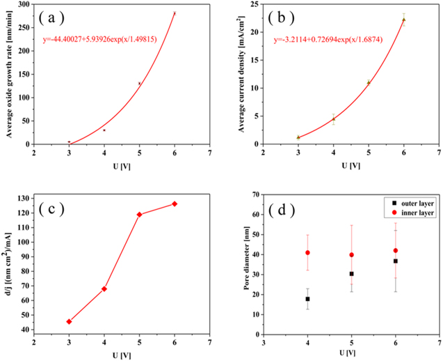
Figure 5. (a) and (b) represent the average oxide growth rate and average current density as a function of potential; (c) the ratio of the thickness of the oxide film on the Sn substrate to the average current density at steady state (d/j) as a function of the potential; (d) variation of pore diameter of porous oxide film with potential.
Download figure:
Standard image High-resolution imageIn addition, an exponential relationship was obtained between the average current density and the anodization potential in Fig. 5b. As mentioned above, the total current density of metal anodization can consist of an electron current density (for the generation of oxygen) and an ion current density (for the generation of oxides).30 In electrolyte systems containing ethylene glycol, the presence of organic substances affects the distribution of potential at the electrolyte/oxide interface, which results in affects the generation of oxygen (Reaction (2a)). If the efficiency of the electron current density was reduced after affecting oxygen, the total current density would be mainly contributed by the ionic current density used to generate the oxide. According to previous reported literature,30 the relationship between the ionic current and potential can be described as

where ji is ionic current density, A and B are temperature dependent constants, and E is the electric field. Ui is the potential drop across the barrier oxide and d is the thickness of barrier oxide. This indicates that the ion current density has an exponential relationship with the potential drop across the barrier oxide. Therefore, in organic electrolytes, an exponential relationship between the average current density and the potential of anodization is reasonable.
Moreover, the anodized tin oxide film obtained on the Sn substrate had a well-difined nanoporous structures (as shown in Figs. 4a–4c). When the potential was lower than 5 V, a crack-free oxide film could be obtained. Even if the potential reaches 6 V, the cracks in the tin oxide film were small (a yellow arrow in Fig. 4f). The formation of transverse cracks in the anodized tin oxide film was related to the generation of excess oxygen.25,31 Figure 5c shows the ratio of the thickness of the tin oxide film to the average current density at steady state (d/j) as a function of the potential after anodization for 10 min. It can be seen that when the potential was lower than 5 V, the growth rate of d/j was gradually increased, and higher than 5 V, the growth rate of d/j was significantly reduced. It is indicated that the proportion of the electronic current used to generate oxygen was significantly increased after the potential was higher than 5 V. The excessive oxygen caused transverse cracks in the oxide film, which is consistent with the result of Figs. 4d–4f.
The anodized tin oxide films with the inner and outer layer structure were also obtained in the range of 4–6 V. The relationship between the average pore diameter of the nanoporous tin oxide films and the potential for anodization was obtained in Fig. 5d. As can be seen, the average pore diameter of the outer layer was increased with the potential, while the pore diameter of the inner layer was independent of the potential of anodization. This fact was in agreement with the data obtained by Zaraska et al.,23 and can be explained as follows. On the one hand, in the initial stage of anodization, the current density increases with potential. The larger amount of charge was allocated for the pore initiation, the more open the porous structure formed. On the other hand, with the increase of the potential of anodization, the rate of oxygen evolution was significantly increased. The aggregation of oxygen bubbles made the nanochannel more open.
Constant potential anodization at 8 V
Figure 6 shows the top and cross-sectional view of the anodized tin film obtained after 5 min of anodization at 8 V. It can be seen that the anodized tin oxide film was still disordered and randomly distributed. Different from the situation of 4–6 V, when the potential was increased, a large number of transverse cracks and voids were found inside the oxide film (yellow arrow in Figs. 6d and 6e). These defects were related to the dramatic evolution of oxygen, which would lead to poor mechanical adhesion of tin oxide films.25 Therefore, the top view of the anodized tin oxide film can see the obvious layered structure (including the inner layer and the outer layer) at a low magnification, as shown in Fig. 6b. Moreover, Figs. 6a and 6c are top views of the inner and outer layers at high magnifications, respectively. The pore diameter of the inner layer was maintained within range of 42 ± 10 nm, and the pore diameter of the outer layer was maintained within a range of 29 ± 8 nm. It is shown that the nanoporous tin oxide films obtained at higher potential also had the morphologies of inner and outer layers. It is worth noting that the outer layer pore diameter of 8 V is lower than 6 V, which is related to the shorter anodizing time at high potential.31
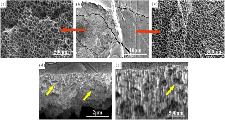
Figure 6. The top and cross-sectional morphology after anodizing 5 min on a tin substrate at 8 V.
Download figure:
Standard image High-resolution imageThe effect of water quality fluctuation on the morphology of the produced anodized tin oxide film was also studied at 8 V. When the volume ratio of ethylene glycol to H2O was changed from 40:60 to 30:70, the morphology of the obtained tin oxide film (as shown in Fig. S1 is available online at stacks.iop.org/JSS/9/104010/mmedia) changed slightly. The oxide film with a large number of transverse cracks was formed on the anode surface, and the inner and outer pore sizes were only slightly increased (as shown in Fig. S3). However, when the volume ratio was 50:50, a relatively uniform surface oxide film could be seen in a low magnification (as shown in Fig. S2a). Meanwhile, nanoporous structure with thicker wall thicknesses could be clearly observed at higher multiples of examination (as shown in Fig. S2b). What's more, the thickness of the oxide layer was only 324 ± 14 nm (as shown in Fig. S2c), which was much smaller than that obtained in the other two electrolytes. It is worthy noted that there were no transverse cracks in the anodized tin film, and the inner and outer pore diameters were also slightly reduced. These results indicate that if the proportion of ethylene glycol in the electrolyte is increased, the adsorption of a larger amount of ethylene glycol on the surface of the anode during the anodization may limit both the growth of oxides and the production of oxygen.
Crystal structure and valence state of anodized tin oxide films
As Padrs et al.14 had reported, although pure tin could be melted at 230 °C, the oxide film on the surface of the Sn substrate retained a porous morphology even at an annealing temperature of 400 °C. The XRD pattern of the as-anodized and annealed at 300 °C is shown in Fig. 7a. The as-anodized film did not show obvious oxide peak, indicating that the tin oxide film was a low-order, amorphous or poorly crystalline material. After annealing the sample at 300 °C, the XRD pattern showed three peaks of the SnO2 phases at 31.8°, 37.8°, and 63.9°, and the peaks of the SnO phase were found at 37.1° and 79.7°. It is indicated that two kinds of tin oxides (SnO and SnO2) could be obtained after annealing the anodized tin oxide film. In addition, a high-intensity Sn peak of the annealed tin oxide film samples was observed at 79.5°, which was caused by the decomposition of the amorphous SnO or SnOx domains in the samples in reactions (3a) and (4a). It has been described in the literature.32–34


Figure 7. XRD (a) and Raman (b) diagrams of anodized tin oxide film before and after annealing obtained at 5 V.
Download figure:
Standard image High-resolution imageInformation on the chemical speciation of the oxide films was obtained by Raman spectroscopy measurements (Fig. 7b). The as-anodized samples did not present strong Raman modes, as expected from their poorly crystalline nature.13 The samples annealed at 300 °C also showed two Raman bands related to SnO phase at 113 and 211 cm−1, and SnO2 phase was shown at 473 cm−1. The results were in agreement with the XRD data previously shown.
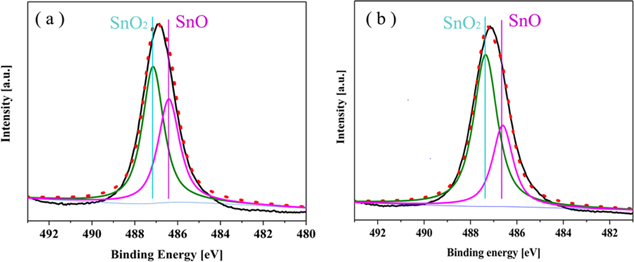
To determine the surface composition of the anodized tin oxide film, the XPS spectra of the as-anodized samples at 3 V and 5 V were recorded. The survey spectra of both sample (not shown here) indicated the presence of Sn and O as well as traces of C on the surface. The content of sulphur and fluorine in the oxide film (below 3 at.%) was relatively small. However, it may be crucial for the formation of porous oxide films. In fact, Hossain et al.35 obtained anodized tin oxide at 4 V in ethylene glycol electrolyte containing 0.1 M NaOH and 0.05 M NH4F, but the morphology of anodized tin oxide was nanoparticles instead of nanoporous structure. And Yang et al.36 have obtained a pompon-like and flower-like microspheres made of SnO nanoflakes via anodization of Sn in a strongly alkaline solution. These studies indicate that the formation of nanoporous anodized tin oxide films in this experiment may be affected by the doping of S2− and F− in the oxide films. However, the mechanism of these two ions on the formation of nanoporous structure of tin oxide film during anodization needs further study. Figures 8a and 8b show the high-resolution Sn3d5/2 spectra of the samples anodized at 3 V and 5 V, respectively. Whether it was 3 V or 5 V, the Sn element had two valence states in tin oxide, which also showed that the obtained anodized tin oxide film was a multivalent mixed oxide layer. And it was confirmed that the ratio of Sn2+ to Sn4+ of the sample formed after anodizing at 5 V for 10 min was 0.62, which was lower than that of the anode film formed at 3 V, which was 0.83. In addition, the content of Sn2+ in the composition of the oxides obtained at lower 2 V was higher (Sn2+/Sn4+ = 0.89), as shown in Fig. S4. Therefore, it can be concluded that the higher potential results in the higher the Sn4+ content in the oxide film. Interestingly, it is different from the results of Zaraska et al.,37 Which may be related to their longer oxidation time at 2 V. In fact, it has been demonstrated on Cu that different valence oxide films can be obtained after anodization at different potentials.38 Therefore, it seems that the valence of Sn in the anodized tin film can be adjusted by adjusting the potential to obtain satisfactory self-doping effect.
Figure 8. The high-resolution Sn3d5/2 spectra of nanoporous tin oxide layers formed by anodization in electrolyte containing F− and S2− at the potential of 3 V (a) and 5 V (b).
Download figure:
Standard image High-resolution image
Conclusions
The relationship between the nanoporous structure of anodized tin oxide films and potential in electrolytes containing F−and S2− were systematically studied in this paper. The critical potentials of the formation of nanoporous structure were analyzed by I–V curves. Combined with potentiostatic anodizing at low potentials (2 V and 3 V), it is shown that the formation of nanoporous tin oxide films was related to the increase of electronic current (for oxygen generation). Meanwhile, oxygen also plays an dominant role in the the change of nanoporous structures with potential. Due to the erosion of electrolyte and the overflow of oxygen, the anodized tin oxide film with constant thickness and adjustable pore size obtained at 3 V was obtained (independent of time). Then, a thick and crack-free anodized tin oxide film could be obtained with the increase of potential. When the potential was higher than 6 V, the transverse cracks related to the excessive oxygen release could be formed. In addition, the obtained tin oxide film with mixed valence states are amorphous, and the content of Sn4+ in the oxide film is increased with the potential.
Acknowledgments
This work was supported by the National key Research and Development Program of China (grant no. 2017YFA0403804).