
Abstract
The influence of morphology on the photoconductive properties of binary ionic porphyrin assemblies is examined. Micro-to millimeter sized crystalline rods and complex hyperbranched structures, or sheaves, were grown in a controlled manner by combining stoichiometric amounts of meso-tetra(4-aminophenyl)porphyrin, H2[H2TAPP]2+, and meso-tetra(4-sulfonatophenyl)porphyrin, [H4TSPP]2−, metal-free ionic tectons. The H2TAPP:H4TSPP structures were characterized by X-ray diffraction, microscopic methods, optical spectroscopy, conductivity and photoconductivity measurements. The two different H2TAPP:H4TSPP morphologies (rods and sheaves) exhibit similar molecular organization and crystal structure but possess different optoelectronic properties. The rods and sheaves exhibit weak dark conductivity and become more conducting upon illumination into the tetrapyroles Soret and Q bands. The primary charge carriers in these solids upon photoexcitation are electrons and the charge recombination mechanism follows monomolecular kinetics. The sheaves also display some persistent photoconductivity, as well as a long "grow in" period of the photoconductivity upon initial illumination. Both of these actions may be attributed to the presence of defects in the sheaves that form during their growth. The measured photoresponse of the H2TAPP:H4TSPP sheaves is higher than that of the rods. This work provides evidence that optoelectronic properties of organic semiconductors can be effectively tuned by controlling their molecular organization and growth morphology.
Export citation and abstract BibTeX RIS

This is an open access article distributed under the terms of the Creative Commons Attribution Non-Commercial No Derivatives 4.0 License (CC BY-NC-ND, http://creativecommons.org/licenses/by-nc-nd/4.0/), which permits non-commercial reuse, distribution, and reproduction in any medium, provided the original work is not changed in any way and is properly cited. For permission for commercial reuse, please email: permissions@ioppublishing.org.
Optoelectronic, chemical, and physical properties of reduced scale (micro and nano) functional materials are determined not only by their composition but also by their morphology.1–3 This morphology or topology is generally controlled during the growth process and is directed by the covalent or noncovalent interactions between the materials' atomic or molecular building blocks. The influence of different morphological forms of crystalline inorganic semiconductors (primarily metal oxides,4–7 and chalcogenides8–10 on their performance in photovoltaics,4,6,8,11,12 sensing,13,14 catalysis15,16 and batteries7,17 has been well documented. In particular, branched and hyperbranched 3D structures with their high aspect ratios were shown to have enhanced photoresponse compared to their 1D or 2D counterparts, where the three different topologies share the same organizational structure and chemical composition.,6,11,12,16,18 For example, ZnO hyperbranched nanostructure exhibited a photocurrent gain of 104 higher than that of a 1D nanorod when both samples were illuminated with a 350 nm laser light.4 Similarly, the hierarchical branched form of CdTe displayed strong photoluminescence that was almost 10-fold more intense than that detected from 1D CdTe nanowires.8
Studies that quantitatively compare optoelectronic properties of organic semiconductors with 3D morphologies and the photoresponse of their lower dimensionality topologies are not readily available.19–21 While 1D and 2D crystalline nanostructures fabricated from π-conjugated molecules are quite common,22–26 3D branched27–29 conductive materials typically assembled from polymers do not always possess well defined crystallinity and morphologies. Ionic porphyrins, a class of highly conjugated organics, are known for forming well-defined multidimensional crystalline structures via self-assembly.30–43 Moreover, recently it was demonstrated that millimeter to nanosized molecular crystalline porphyrin solids can be fabricated in a controlled and reproducible manner with tunable structures and morphology.44 This synthetic advancement has provided a more systematic approach for quantitatively evaluating and comparing optoelectronic behavior of porphyrin (and other organic) crystalline solids with similar structure but different topology.
In this work, we report a detailed comparison of the optoelectronic properties of two structurally identical but morphologically different forms of a binary porphyrin (BP) system composed of meso-tetrapyridyl porphyrin H2[H2TPyP]2+ and [H4TSPP]2− ionic tectons, H2TAPP:H4TSPP (Fig. 1). Micro- and nanostructures 1D rods and 3D hyperbranched sheaves of H2TAPP:H4TSPP were synthesized in a controlled manner using the growth algorithm reported earlier. Eskelsen and coworkers were the first to prepare a crystalline hyperbranched 3D H2TAPP:H4TSPP nanostructure with well-defined sheaf-like morphology39 that structurally emulate the hyperbranched structures made from inorganics.45 Eskelsen initially proposed a potential crystal structure for the H2TAPP:H4TSPP sheaves based on data from selected area electron diffraction (SAED) and X-ray powder diffraction.39,46 Later, Adenehnia et al.41,47 reported that the powder X-ray diffraction patterns obtained from H2TAPP:H4TSPP sheaves and rods indicate that both morphological types have the same molecular structural geometry.48–50 Here, we present combined conductivity and photoconductivity measurements of H2TAPP:H4TSPP rod and sheave structures and analyze the dynamics of photoexcitation. The results of our studies support an enhanced photoelectrical responsivity in 3D H2TAPP:H4TSPP compared to their 1D crystalline morphology.

Figure 1. Structures of the ionic tectons, H2[H2TPyP]2+ (left) and [H4TSPP]2− (right) present in the H2TAPP:H4TSPP crystals fabricated under controlled growth conditions in the pH 3.6 − 2.9 range.
Download figure:
Standard image High-resolution imageExperimental
Materials and synthesis
Porphyrin tectons, meso-tetra(4-aminophenyl)porphyrin and meso-tetra(4-sulfonatophenyl)porphyrin dichloride, both 99% pure, were purchased from Frontier Scientific and used without further purification.
The H2TAPP:H4TSPP crystals were prepared in an acidic aqueous media (pH 2.9 for sheaves and pH 3.6 for rods) from ionic tectons H2[H2TAPP]2+ and [H4TSPP]2- in a 1:1 ratio, respectively. Details of the synthetic and isolation procedures are described elsewhere.39,41,44 The product moniker, H2[H2TAPP]:[H4TSPP], reflects the numbers of protons associated with the core nitrogens and additional protons on the heterocycle substituents in the constituent porphyrin ions (Fig. 1). For brevity, the abbreviated name, H2TAPP:H4TSPP, will be used for the BP crystals in this work.
SEM
H2TAPP:H4TSPP samples were deposited from solution onto glass coverslips (10 mm diameter, Ted Pella Inc.) and allowed to dry in vacuum overnight. The glass pieces were attached to an aluminum SEM stub using double stick electrical conductive carbon tape and then were coated with a layer of gold (5–7 nm) using a Technics Hummer V sputter coater. Micrographs were obtained with a FEI Quanta 200 F SEM at 10 mm working distance and 30 kV beam energy. The instrument working pressure was 10−6 Torr.
AFM
Imaging specimen were prepared by depositing 1 or 2 drops of the H2TAPP:H4TSPP crystals solution onto freshly peeled HOPG for 1 min followed by a 30 s spin at 3900 rpm. This process was repeated several times to create a well dispersed sample for AFM imaging. H2TAPP:H4TSPP crystals were imaged with a Bruker Multimode 8 Atomic Force Microscope using TAP150 tips (antimony doped silicon cantilever with driving frequency of 150 MHz and force constant of 450 N/m purchased form Bruker). Images were collected in tapping mode.
X-ray diffraction
Powder X-ray diffraction (XRD) analysis was performed to evaluate the crystallinity of the H2TAPP:H4TSPP structures. The crystalline porphyrin samples were analyzed in a SmartLab (Rigaku) diffractometer (Cu Kα radiation—D/tex ultra linear position sensitive detector) in parallel beam configuration. Diffraction patterns were obtained in the range of 4–30 2θ degrees at a scan rate of 1.5° min−1.
UV–visible diffuse reflectance spectroscopy (DRS)
Samples were prepared by grinding small amount of TAPP, TSPP and H2TAPP:H4TSPP with KBr such that the final concentration of the porphyrin was about 0.2 wt% in each of the samples. The powders were loosely pressed in a metal anvil cell with a 1 cm quartz window. Reflectance spectra were collected using a ThermoFisher Bio 260 UV–vis Spectrophotometer equipped with an ISA-220 integrating sphere. All reflectance data was processed using the Kubelka-Munk transform.
Interdigitated electrodes (IDE) preparation and treatment
Gold IDEs with a spacing of 10 μm were used for the conductivity experiments were fabricated per specifications by the University of California at Santa Barbara Nanofabrication Facility. Two variations of the IDEs were used; the first were Au electrodes fabricated directly on glass, the second were fabricated on top of a 400 nm thick SiO2 layer supported on a p++ doped silicon chip. The glass IDEs were used for most conductivity experiments so samples could be illuminated from the side on which they made contacts with the Au electrodes while the IDEs on the silicon chips were used for performing field effect experiments. BP crystals of known concentration were deposited on the IDEs by placing a drop liquid suspension atop the IDE, allowing the solution to sit for an hour, and then wicking away any excess with a Kimwipe tissue. The IDE was then examined under an optical microscope to determine if a sufficient number of porphyrin crystals were present on the IDE. This process was repeated until an acceptable number of rods (averaging between 50 and 70) had been deposited. A more detailed procedure for IDE doping is described elsewhere.36,37,51
Photoconductivity measurements
Action spectra, time dependence, temperature dependence, and field effect experiments were measured in an in-house designed vacuum chamber with a base pressure <5 mTorr.51 Prior to all measurements, samples were heated to 373 K under vacuum for at least 12 h. Source-drain biases (VSD) were applied using a Data Translation DT9836 data acquisition system (DAQ). The current was measured using a Keithley 427 current amplifier and recorded by the DT9836 DAQ. A Keithley 246 high voltage supply was used to apply gate voltages (VG). Variable power 406, 445, 473, 671 nm, and 785 nm diode lasers and a 632.8 nm HeNe laser were used as excitation sources. These wavelengths were selected based on the measured absorbance spectra of the H2TAPP:H4TSPP crystals. The laser beams were focused to a 1 mm diameter spot size. A calibrated photodiode was used to monitor the laser power during all experiments. Illumination experiments were performed using a Measure Foundry (Data Translation, Inc.) program designed to control and record VSD and record the time, current, and photodiode signal.
Current-time (I-t) curves were collected by applying VSD = 5 V and VG = 0 V while recording the current. A baseline was measured for 1000 s in the dark, and then the sample was illuminated with 406, 445, or 785 nm irradiation until saturation current was reached. Illumination was then terminated, but measurement of the current continued for at least 30 min. These experiments were performed at 298, 323, 348, and 373 K.
Results and Discussion
Morphological control
H2TAPP:H4TSPP crystalline assemblies were prepared using a nucleation and growth model developed by us earlier.44 Parent TAPP and TSPP monomers were combined at pH 2.9 and pH 3.6 to produce rods and sheaves, respectively. Within this hydrogen ion concentration range the expected charges in solution on the TAPP are +2 and the TSPP ion −2.39,52,53 In the H2TAPP:H4TSPP crystal the porphyrin dication is in a free-base form while the dianion exists as a diacid.47
SEM micrographs revealed that the H2TAPP:H4TSPP rods have rectangular cross sections (Fig. 2a) and are about 1 mm in length. The AFM images specify typical rod's height as greater than 100 nm. The sheaf-like, or hyperbranched, H2TAPP:H4TSPP structures (Figs. 2b and 2c) are composed intercrossing ribbons 50 nm tall and 180 nm wide.39 The bundles are typically microns long and have no clear definition of the growth origin due to crystal splitting during the initial oriented attachment (OA) growth followed by Ostwald ripening.54 This type of growth process has been observed in other hyperbranched and sheaf-like systems.50
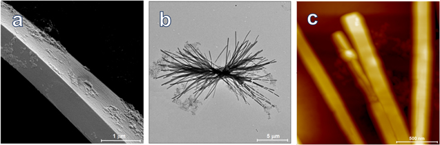
Figure 2. Micrographs of the H2TAPP:H4TSPP structures: (a) SEM image of a typical rod (Reproduced in part from Ref. 25. Copyright American Chemical Society.), (b) SEM of a sheaf bundle, and (c) tapping mode AFM image of sheaf ribbons, Ref. 47. The sheaf ribbons in (c) are 40–60 nm tall; sheaves were deposited on HOPG.
Download figure:
Standard image High-resolution imagePowder X-ray diffraction patterns obtained from H2TAPP:H4TSPP sheaves and rods were nearly identical, indicating that both morphologies share the same crystal structure (Fig. 3). The observed peak intensity differences are due to preferential orientation in the two types of H2TAPP:H4TSPP morphologies. Both crystal systems belong to orthorhombic Pnn2 space group with unit cell dimensions of a = 30.88 Å, b = 15.45 Å and c = 7.98 Å; α = β = γ = 90° (Fig. 4).39,41,47 Face-to-face arrangement of alternating oppositely charged tectons forms highly coherent columns.
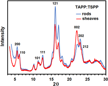
Figure 3. Comparison of powder X-ray diffraction patterns obtained from H2TAPP:H4TSPP crystalline rods and sheaves.
Download figure:
Standard image High-resolution image
Figure 4. Crystal structure of H2TAPP:H4TSPP in two different orientations: direction normal to the crystallographic c axis (top) and direction normal to the crystallographic b axis (bottom). Bottom view depicts the growth direction of the rods with alternating cationic and anionic porphyrin tectons within the columns. Molecular structures' color code: H2[H2TAPP]2+, blue and [H4TSPP]2−, red. Adopted in part from Ref. 46.
Download figure:
Standard image High-resolution imageOptical spectra, conductivity, and photoconductivity measurements
Figure 5a depicts the solid state UV–vis absorption spectra of TAPP and TSPP parent tectons (as purchased). The TSPP spectrum has two strong absorbances in the Soret region at 415 nm and 490 nm. The 415 nm transition is due to the non-aggregated porphyrin. Because the TSPP material was acquired as an HCl adduct the red shifted maximum is due to the presence of an aggregated (J-aggregate),55,56 form of the tecton.

Figure 5. Diffuse reflectance UV–vis spectra of TAPP and TSPP parent porphyrins (a) and H2TAPP:H4TSPP rods and sheaves (b).
Download figure:
Standard image High-resolution imageThe diffuse reflectance spectra (DRS) of the H2TAPP:H4TSPP rods and sheaves have similar profiles, including a sharp Soret absorption around 420 nm and a broad Q-band extending into the near IR (around 800 nm). This near IR band is due to a hyperporphyrin character of the TAPP ion.52,57 Small shoulders on both the Soret (right side) and Q-bands (left side) of the sheaves spectrum, may be due to possible traces of small clusters of TSPP J-aggregates55,56 and unreacted TAPP molecules,52,57 respectively. However, X-ray photoelectron spectroscopy and elemental analysis (both not shown here), support a 1:1 composition of H2TAPP:H4TSPP of both the rod and sheave structures.47 Thus, the amounts of unreacted parent porphyrins in these structures have to be negligible.
H2TAPP:H4TSPP crystals optoelectronic response measurements conducted on tens of different samples with each sample being measured in triplicate. The measurements were not significantly affected by size of the crystals investigated but were sensitive to the number of contacts the rods and sheaves made with the IDE electrodes and, therefore, sample preparation played a significant role in the overall signal observed. Great care was taken to prepare all IDE samples as reproducibly as possible. Each specimen was inspected under an optical microscope for uniformity before continuing with measurements. Although the magnitudes of the currents and photocurrents varied with the specimen coverage of the IDEs, the final calculated conductivities and photoconductivities were all similar.
Unlike other metal-free binary porphyrin materials we investigated earlier, which do not conduct in the absence of illumination,36–38,47 the H2TAPP:H4TSPP rods and sheaves both exhibit weak dark conductivity. The conductivity of these crystals was determined using the formula:

where σ is the conductivity; V is the voltage applied to the sample; I is the measured current and L is the length of the spacing for the interdigitated electrodes. The cross-sectional area, A, of a typical sample was about 300 square microns and was determined by multiplying the average height of the rods/branches by the average width of the rods/branches and finally by number the rods/branches on an IDE (estimated error is ±10%).The calculated conductivity of the rods and sheaves was 1.0 × 10⁻⁸ S·m−1 and 5.6 × 10⁻⁹ S·m−1, respectively. The conductivity of both morphological systems increases with increasing temperature (Fig. S1 is available online at stacks.iop.org/JSS/9/061010/mmedia in the Supplementary Material) according to an Arrhenius expression:
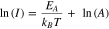
where EA is the activation energy of the conduction process, kB is Boltzmann's constant and A is the pre-exponential factor. Measurements of the conductivity at various temperatures were fit to Eq. 2 and the activation energies were extracted. For the sheaves, the activation energy (EA) is 525 meV while for the rods EA = 274 meV (Table I).
Table I. Comparison of the activation energies the dark conductivity and photoconductivity processes (at 406 nm and 785 nm laser illumination) for the H2TAPP:H4TSPP sheaves and rods.
| H2TAPP:H4TSPP morphology | Activation energy, EA (meV) | ||
|---|---|---|---|
| Dark conductivity | PC | ||
| 406 nm | 785 nm | ||
| rods | 274 | 313 | 318 |
| sheaves | 525 | 107 | 232 |
Quantifiable dark conductivity of the H2TAPP:H4TSPP sheaves and rods may be attributed to their strong absorbances in the near infrared. The relatively narrow 1.3 eV π−π* band gap (EG) of the H2TAPP:H4TSPP crystals support increased conductance and the observed dark current. Other BP materials studied in our laboratory had higher values of EG (∼1.7 eV)47 and did not conduct in the dark (Table II). The lower dark current density for the H2TAPP:H4TSPP sheaves (compared to the rods) can be related to the sheaf resistance caused by defects or impurities, which act as charge carrier traps. The number of these defects or traps is expected to be higher in the sheaves' morphology which is produced by a crystal splitting growth process.39,54 Crystal splitting is associated with fast crystal growth but can also result from defects and stresses.39,54
Table II. Comparison of optical, dark conductivity, and photoconductivity (NPC and PPC) of metal free binary porphyrins crystalline solids. Included are room temperature photoconductance values, σ (Ω−1 m−1). Laser intensity was 1.0 mW cm−2.
| Porphyrin System | Tecton separation (Å) | π−π*band gap (eV) | Dark conductivity (Ω−1 m−1) | NPC | PPC | PC (Ω−1 m−1) |
|---|---|---|---|---|---|---|
| H2TMPyP:H2TSPP rodsa) | 4.16 | 1.72 | no | yes | Soret | 4.0 × 10⁻⁸ |
| H2TPyP: H4TSPP rodsb) | 4.31 | 1.63 | no | yes | Q and Soret | 9.3 × 10⁻⁸ |
| H2TAPP: H4TSPP rods | 3.99 | 1.33 | 1.0 × 10⁻⁸ | yes | no | 1.6 × 10⁻⁷ |
| H2TAPP:H4TSPP sheaves | 3.99 | 1.33 | 5.6 × 10⁻⁹ | yes | Q and Soret | 2.2 × 10⁻⁷ |
A comparison of the photoconductivity action spectra with absorbance spectra of H2TAPP:H4TSPP rods and sheaves are shown in Figs. 6a and 6b. The similarities of the two sets of spectra suggest that the number of electrons contributing to the photocurrent is directly proportional to the number of photons absorbed by the H2TAPP:H4TSPP rod and sheaves, respectively. Additionally, the power dependences of the photoconductivity (Fig. S2 in Supplementary Material) of the rod and sheaves are linear, further supporting the hypothesis that the number of electrons contributing to the photocurrent of each morphological system is directly proportional to the number of photons absorbed by the H2TAPP:H4TSPP crystals.
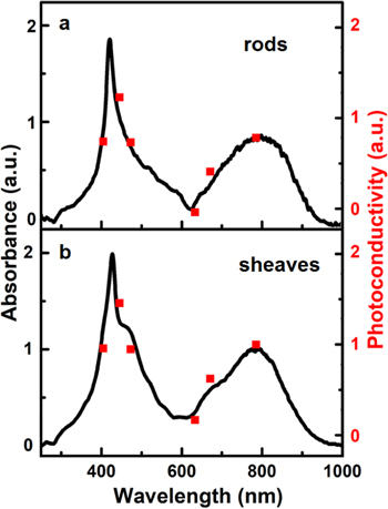
Figure 6. Photoconductivity action spectra of the H2TAPP:H4TSPP nanorods (a) and (b) sheaves.
Download figure:
Standard image High-resolution imageFigure 7 shows the current-voltage (I-V) dependence of the H2TAPP:H4TSPP rods and sheaves in the dark and under illumination. The I-V characters are symmetric for both types of morphologial samples, the nearly linear current-voltage dependence of the sheaves indicates a more ohmic behavior than that of rods under the same experimental conditions. Illumination of both the H2TAPP:H4TSPP rods and sheaves increases the population of electrons in their respective conduction bands, thereby increasing conductivity. This conduction mechanism is not related to the charge-transfer exciton pathway reported for porphyrin systems that only become conductive when exposed to a light source.36–38,47,58 Like every BP we have studied thus far the H2TAPP:H4TSPP system is also an n-type photoconductor.36–38,47 The recombination mechanism of the photogenerated charge carriers in the H2TAPP:H4TSPP was estimated from plots of photocurrent (I) variation with laser power (P) plots for these systems (Fig. S2 in the Supplementary Material). A power law dependence relationship of I ∝ Pa yielded a value of a ≈ 1 which is consistent with unimolecular (geminate) recombination mechanism.59–61 Unimolecular kinetics involve the recombination of one free carrier at a time (e.g. an electron captured by a recombination center and then recombined with a hole; carrier loss to electrodes or to a trap) primarily originating from trapping of charge.
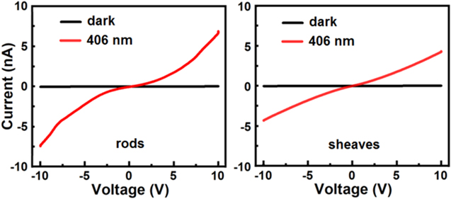
Figure 7. Current–voltage characteristics of the H2TAPP:H4TSPP rods and sheaves measured in the dark (black line) and under 8 mW 405 nm illumination (red line).
Download figure:
Standard image High-resolution imageThe conductivities of the H2TAPP:H4TSPP rods and sheaves under 406 nm excitation are collected in Table II. The calculated illuminated conductivity of the rods was 1.6 × 10⁻⁷ S·m−1 while that of the sheaves was at 2.2 × 10⁻⁷ S·m−1. The sheaves are ∼40% more conductive as the rods. Furthermore, PC values are much higher (order or two of magnitude) than the photoresponse of H2TMPyP:H2TSPP (and its metallated modifications) and H2TPyP:H4TSPP crystals (Table II). The higher conductivity and photoconductivity values of the H2TAPP:H4TSPP crystals can be related to their low bandgap (Table II) and reduced distance between the ionic tectons in the crystal structure compared to the same parameters for the other BPs studied (Table II). Smaller size of the cationic ring substituents (−HN2), facilitate smaller intermolecular separation of the ionic tectons and the direct face to face π−π overlap of the chromophores increases charge transport. Finally, the red shift in the absorption of [H2TAPP]2+ relative to the other cations ([H2TMPyP]2+ and [H2TPyP]2+) suggests a greater electron affinity which also lowers the band gap.
The measured conductivity values for the H2TPyP:H4TSPP crystals are higher or comparable to the amounts (ranging from ∼10−12 to ∼10−7 Ω−1 m−1) reported for many other ionic and neutral porphyrin-based solids (the actual structure for most of those materials has not been uniquely determined).43 There are, however, some exceptions. Nanorods composed of zwitterionic H2[H2TSPP] while insulating in the dark displayed a photoconductivity signal of 6.4 × 10⁻⁵ Ω−1 m−1 (on exposure to 488.0 nm laser light).30 A 2:1 ratio of SnTPyP4+ and H4TSPP2− of ionic tectons formed nanotubes with reported photoresponse of 3.1 × 10⁻⁴ S m−1.43 A filtered Xe arc lamp (390–630 nm) with illumination power of 29 mW cm−2 was used for photoexcitation. No crystal structures of H2[H2TSPP] or 2[SnTPyP]:[H4TSPP] have been reported.30,43
Temperature dependent photoconductance of H2TAPP:H4TSPP crystals (like their dark conductivity) follow an Arrhenius behavior that can be described by Eq. 2. Activation energies obtained for the rods and sheaves, for photoexcitation carried out with 785 nm and 406 nm laser lines are listed in Table I.
Figure 8 shows the photoconductive temporal responses of the H2TAPP:H4TSPP sheaves and rods under 406 nm and 785 nm photoexcitation. The rods exhibit a prompt response to both excitation wavelengths. The sheaves have a higher current density than the rods at least by a factor of two with both 785 nm and at 406 nm illumination but a non-linear time response. When the laser is first turned on, there is a sharp increase in current that accounts for only about 70% of the maximum current measured during illumination. After this initial jump, there is a gradual increase in current over several thousand seconds. When illumination stops, 90% of the current goes away immediately, but that last 10% persists for hundreds of seconds.
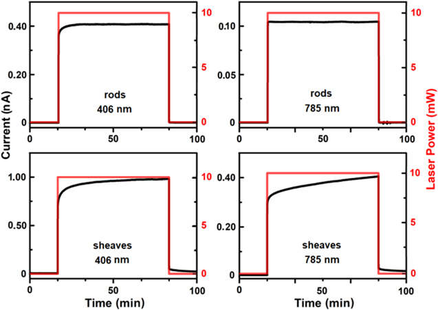
Figure 8. Comparison of the photoconductive response of H2TPyP:H4TSPP rods and sheaves in a vacuum environment (5 mTorr) and 406 nm 785 nm excitation.
Download figure:
Standard image High-resolution imageThis behavior, known as persistent photoconductivity (PPC), has been observed in H2[H2TSPP]30 and in H2TMPyP:H2TSPP and H2TPyP:H2TSPP systems by Borders and Van Zijll.36,37 As with the other porphyrin systems that exhibit PPC, the current decays can be fit with a stretched exponential fit:
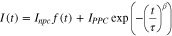
where Inpc is the non-persistent photocurrent; f(t) is a time dependent function describing the time dependence of the non-persistent current, which are primarily due to the response times of the electronics used to make the measurements; IPPC is the persistent photoconductivity; τ is a weighted average lifetime; and β is the stretching factor.38,62 Excitation at 406 nm yields τ = 278 s and β = 0.26 whereas excitation at 785 nm yields τ = 1927 s and β = 0.17. For semiconducting materials with PPC decay, some authors have associated the value of β with the dimensionality of the charge transport process.38,63,64 For a one-dimensional transport process, β < 0.5. For the H2TAPP:H4TSPP sheaves a suggesting a one-dimensional charge transfer process mechanism is consistent with the proposed face-to-face stacking of the [H2TAPP]2+ and [H4TSPP]2− ions along the length of the nanorods.
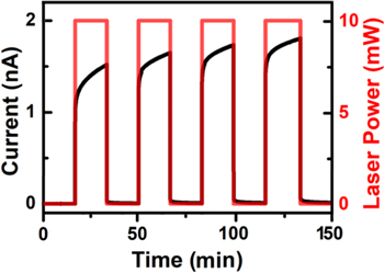
To further examine the nature of the time dependent increase in the photoconductivity of the H2TAPP:H4TSPP sheaves observed in Fig. 8, the photocurrent growth and decay times were evaluated by periodic turning on and off (1000 s for each action) of the 406 nm laser under a constant 5 V bias (VSD). The results are depicted in Fig. 9. Here, the sharp rise in the current increases with each cycle of illumination, while the amount of decay (PPC) after each cycle remains approximately the same. The difference between the initial current rise with each subsequent cycle of exposure to light was smaller, suggesting that conductivity is approaching a maximum value, which is consistent with eventual maximization of the current at ∼ 200 min), observed in Fig. 8 (also see Fig. S4 in Supplementary Material).
Figure 9. Time dependent photoconductivity of the H2TAPP:H4TSPP sheaves subjected to alternating 1000 s periods of dark/illumination (406 nm laser). The profile of each illumination cycle shows a similar initial upsurge in current following a dark current period before the next exposure to light.
Download figure:
Standard image High-resolution image
The difference in optoelectronic properties of H2TAPP:H4TSPP the rods and the sheaves, can be attributed directly to the difference in their morphology since their crystal structures are the same. By the nature of their fast growth mechanism (discussed earlier), the sheaves are expected to possess a greater number of defects and stresses, which act as charge carrier traps. In semiconductors, surface or near-surface defects or impurities may act as electron or hole traps. The photoexcited electrons or holes may be confined in these trap states and then recombine with holes usually at the top of the valence band and emit photons. The deeper trap states tend to recombine non-radiatively by emitting phonons.4,13,65,66 Thus, when the laser light is first turned on, the defect states in the H2TAPP:H4TSPP sheaves are mostly unoccupied. Many of the electrons that are excited into the conduction band fall into the low energy defect states and become immobilized. A high concentration of defects lowers the mean free path of the charge carries moving through the solid, resulting in a quenched photocurrent. As more of the defect states become populated populate, the mean free path of the charge carriers increases, resulting in increased current. When the illumination is removed shuts off, most of the current dissipates as electrons are no long being excited into the conduction band. The observed persistent conductivity is likely a result of the slow depopulation of the defect states via thermal excitation into the conduction band. A similar mechanism was used to describe the persistent photoconductivity in ZnO branched and 1D structures.4,67
The lower dark current of the H2TAPP:H4TSPP sheaves (compared to the dark conductance of the rods) is attributed to the same defects responsible for the difference in their photoconductive behavior. The dark conductivity of the sheaves has significantly higher activation energy than the dark conductivity of the rods. This is likely a result of the decreased mobility of the electrons within the sheaves due to the presence of the defects. The sheaves need not only energy to thermally excite electrons into the conduction band, but also to release electrons trapped within the defect states.
Conclusions
In this work we demonstrated that the morphology of a BP crystalline system, H2TAPP:H4TSPP influences their optoelectronic properties. Rods and sheaf-like structures of the BP were grown reproducibly under controlled conditions and share the molecular organization and the same crystal structure. This crystal structure consists of porphyrin macrocycles (alternating [H2TAPP]2+ free base species and [H4TSPP]2− diacid) aligned cofacially in columns along the c crystallographic axis via ionic bonding, hydrogen bonding, and π−π interaction.
The UV–vis spectra of the rods and sheaves are similar and exhibit broad Q-bands that extend well into the near IR. Optical band gap of H2TAPP:H4TSPP is narrower (1.3 eV) compared to EG (∼1.7 eV) in most of the other BP systems we have studied.47 Both H2TAPP:H4TSPP sheaves and rods conduct weakly in the dark and become photoconducting when exposed to laser light. The photoconductive response of the rods is fast and occurs with excitations into either the Q or Soret bands. The sheaves are almost twice as photoconductive as the rods but their photoresponse is slower than that of the rods; sheaves exhibit PPC while the rods to not. The divergent optoelectronic behavior of sheaves may be attributed to defects associated with their growth morphology. Overall the results presented here support an enhanced photoresponse in 3D hyperbranched H2TAPP:H4TSPP topology compared to their 1D morphology.
The relatively narrow optical band gap, the presence of dark current, and the variance in the photoresponse of the H2TAPP:H4TSPP sheaves and rods make them particularly interesting for future studies. In order to increase the PC one would need to further decrease the band gap of the porphyrin ion pair by increasing the electron affinity of the negative tecton and decreasing the ionization potential of the cation. The addition of a metal to the cores of parent porphyrins may accomplish that goal. In earlier work we demonstrated that inclusion of a metal in the core of one of the BPs preserves the geometrical structure of the metal-free parent crystal system but modifies its photoresponsivity.37,47 Computational modeling can be used to provide guidance for optimizing photoresponse with judicious selection of metal substituents.
Acknowledgments
We thank the National Science foundation for their support of this work in the form of grant CHE-1152951 and the Francheschi Microscopy and Imaging Center at Washington State University for the use of their SEM facilities. The assistance of Dr. J. R. Eskelsen and Dr. M. Adinehnia with some of the data collection and analysis is much appreciated. Finally, we enthusiastically acknowledge and applaud the inspiring lifelong commitment of Professor Karl Kadish to the advancement and dissemination of the science of porphyrins and phthalocyanines through his work with the Electrochemical Society and his editing of the seminal Journal of Porphyrins and Phthalocyanines and the Handbook of Porphyrin Science.