
Abstract
In the present work, effect of swift heavy ion (SHI) irradiation on structural and optical properties of β-Ga2O3 thin films was investigated. Different ion fluences (ϕ) of 120 MeV Ag9+ ions ranging from 1 × 10¹¹ ions-cm−2 to 5 × 10¹² ions-cm−2 were employed. The films were grown at room temperature (RT) using electron beam evaporation method and post-deposition annealing was done at 900 °C in oxygen atmosphere. X-ray diffraction (XRD) and UV–visible (UV-Vis) spectroscopy data confirmed the formation of polycrystalline β-Ga2O3 phase having a bandgap of ∼5.14 eV. An increase in the structural disorder, and decrease in the average crystallites size of β-Ga2O3 with increasing ϕ was also revealed by XRD. Ga2O3 thin films showed high transparency in the UV (upto 280 nm) and visible range with average transmittance of ∼80%. Rutherford backscattering spectrometry (RBS) revealed that the thin films were slightly O deficient. A low frequency vibration mode at 170 cm−1 arising from liberation and translation of tetrahedra-octahedra chains in β-Ga2O3 was observed through Raman spectroscopy. Scanning electron micrograph (SEM) images suggested that the films were fairly smooth.
Export citation and abstract BibTeX RIS

This is an open access article distributed under the terms of the Creative Commons Attribution 4.0 License (CC BY, http://creativecommons.org/licenses/by/4.0/), which permits unrestricted reuse of the work in any medium, provided the original work is properly cited.
In the recent years, β-Ga2O3 has received considerable scientific attention as a promising semiconductor material. It is well known for its wide band gap (∼4.9 eV) and high estimated critical electric field strength (∼8 MV cm−1) which could allow operation of β-Ga2O3 based devices in high temperature and high voltage environments.1 It has a monoclinic crystal structure and belongs to C2/m space group.2 It has found diverse applications such as gas sensors,3–5 deep UV solar blind photodetectors,6,7 chemical sensing and catalysis,8–10 and electroluminescent devices.11,12 In wide-bandgap semiconductors, the defects in the crystal structure create some additional levels that can act as acceptors or donors.13 These defects are often caused by irradiation damage due to fluxes of highly energetic protons, electrons, α-particles, and γ-rays etc. During ion irradiation, damage in the material can cause various changes like amorphization and stress in the microstructure, diffusion of dopants, introduction of trap states etc.14 These changes determine the physical properties of the material. Wide-bandgap semiconductors possess strong atomic bonding which makes them radiation resistant.15 The radiation hardness becomes a decisive factor for a material to survive in strong radiation zone for military and space applications. The β-Ga2O3 is one such promising wide-bandgap semiconductor material which is both chemically and thermally stable, and may survive in radiation hard atmosphere.
To understand the response of β-Ga2O3 to ion irradiation in high-energy region is of particular importance for the development of nuclear fuels16 and electronic devices for spacecraft17 which are continuously irradiated by energetic nuclear fission fragments and by cosmic rays respectively. It is being noted that for space-based applications, the energy of heavy ions lies mostly in the MeV range.18,19 This may be due to the fact that the Earth's atmosphere receives radiation consisting of charged particles like electrons and protons with their energy being in the range from few MeV to several hundred MeV.15 Therefore, understanding the effects of energetic (in MeV range) ion bombardment on β-Ga2O3 thin films will be useful in simulating the behaviour of the devices based on this material under radiation environment. Earlier, Kim et al.15 have shown the effects of radiation damage due to electron, proton and neutron on β-Ga2O3 materials and devices. Proton (10 MeV) irradiation led to the suppression of drain current in transistors and generation of trap states in rectifiers. Liu et al.20 have shown the effects of 25 MeV O4+ ion irradiation on the structural and optical properties of n-type single crystal β-Ga2O3 with ϕ varying from 1.5 × 10¹¹ to 1.5 × 10¹² ions-cm−2 led to generation of deep levels due to divacancies, and trapping of charge carriers along with production of non-radiative recombination centres at high ϕ values. In this article, a thorough, systematic investigation on the effect of 120 MeV Ag9+ ion irradiation at different ϕ on β-Ga2O3 thin films using XRD, SEM, UV–vis, RBS and Raman Spectroscopy is carried out.
Experimental
Ga2O3 thin films of thickness ∼400 nm were grown on silicon and quartz substrates (∼10 mm×10 mm each) by means of electron beam evaporation method in a high vacuum chamber (∼3 × 10⁻⁶ Torr) at target lab, Inter-University Accelerator Centre (IUAC), New Delhi. Prior to the deposition, substrates were cleaned for organic contamination with trichloroethylene solution followed by acetone, isopropanol and water for 5 min each, and then mounted on a sample holder inside the chamber. Small pellets of high-purity (99.99%) Ga2O3 were taken as evaporation material. The thickness of the film was measured with a quartz crystal monitor. After deposition, thin films were annealed at 900°C for 30 min under oxygen environment to obtain crystalline phase. The flow rate of oxygen during annealing was 200 ml min−1. SHI irradiation was carried out using 120 MeV Ag9+ ions with ϕ of 1 × 10¹¹ ions-cm−2, 3 × 10¹¹ ions-cm−2, 5 × 10¹¹ ions-cm−2, 1 × 10¹² ions-cm−2 and 5 × 10¹² ions-cm−2, using 15 MV pelletron accelerator facility of IUAC, New Delhi. The ion flux was 6.25 × 10⁹ ions-cm−2 s−1. The samples were mounted on a copper holder using conductive silver paste to reduce the sample heating. The beam was magnetically scanned on the sample surface for uniform irradiation. One of the samples annealed at 900 °C was left un-irradiated and used as the pristine sample. SRIM (stopping range of ions in matter) software was used to estimate electronic energy loss per unit length (Se), nuclear energy loss per unit length (Sn), and the range of the irradiated ions. For 120 MeV Ag9+ ion irradiation on Ga2O3, Se and Sn were calculated to be 25.19 and 0.118 keV nm−1, respectively, at the surface of the thin film. Variation of the Se and Sn with depth inside the thin film and the substrate is shown in Fig. 1. The projected ion range was estimated to be 17.04 μm.

Figure 1. Variation of Se and Sn with depth for Ga2O3 thin films grown on silicon substrates.
Download figure:
Standard image High-resolution imageAfter ion irradiation, both pristine and irradiated samples were characterized by XRD measurements using PANalytical empyrean diffractometer with CuKα source. UV–visible optical transmission spectra for the samples were obtained using Hitachi-3300 UV–vis spectrophotometer working in the wavelength range from 200 to 800 nm. The SEM analysis was performed using an FEI Quanta 200. RBS measurements of the samples were performed with 2 MeV 4He+ ions using NEC's 5SDH-21.7 MV Pelletron accelerator facility of IUAC, New Delhi. The total charge collected was 10 μC. The XRUMP simulation software was used to analyse the RBS data to obtain thickness and elemental composition of the films.21 Micro-Raman spectroscopic measurements were performed at RT using Renishaw invia Raman spectrometer with 514 nm He-Ne laser used for excitation.
Results
The film thickness and composition of the grown thin films were determined by RBS. Figure 2a shows the RBS spectra of as–grown, annealed (pristine), and ion irradiated thin film sample at ϕ = 1 × 10¹² ions-cm−2. Similar spectra were also observed for all ϕ. The peaks at channel no. 680 and 1564 belong to O and Ga, respectively, arising due to the two constituents of the thin films. The plateau caused by scattering of He+ ions from Si substrate is also seen up to channel no. ∼900. From the simulations (Fig. 2b), composition of the thin films was found to be 41 atomic % of Ga and 59 atomic % of O in all the samples. The ratio O/Ga is 1.43 which is slightly less than 1.5 the value expected for stoichiometric Ga2O3 thin films. The thickness of as–grown thin films was found to be 420 nm. The thickness decreased to a value of 380 nm after annealing at 900 °C along with a decrease in the intensity of Ga peak. The intensity of Ga peak remains constant under ion irradiation. The reduction in thickness can occur due to compacting and shrinkage of the thin films under annealing.22

Figure 2. (a) RBS spectra of as-grown, 900 °C annealed and irradiated sample with ϕ = 1 × 10¹² ions-cm−2. (b) The experimental and simulated RBS spectra are shown with black and red line respectively.
Download figure:
Standard image High-resolution imageThe XRD patterns of as-grown and irradiated samples deposited on silicon substrate are shown in Fig. 3a. The patterns correspond to monoclinic β-phase gallium oxide (space group C2/m) with identified peaks (400), ( 01), (002), (
 12) and (
 01) lying at 2θ values of 30.05°, 30.49°, 31.74°, 43.35° and 44.20°, respectively.22–25 The narrow peak at 2θ ∼33.5° can be assigned to the diffraction from (111) plane of Si substrate. These peak values are in good agreement with the Joint Committee on Powder Diffraction Standards card no. 41-1103, and confirm the formation of polycrystalline β-Ga2O3 in the thin film. Moreover the observed peaks did not match with the XRD peaks of polymorphs of Ga2O3 (α-, γ-, δ-, ε-) other than β-phase.26,27 The peak (400) with highest intensity was used to determine the average crystallites size (D) of the samples. To determine D, Debye–Scherrer formula (given below) was used:

Where λ is the wavelength of the X-ray radiation, θ is the incident angle and B represents the FWHM of the diffracted peak.
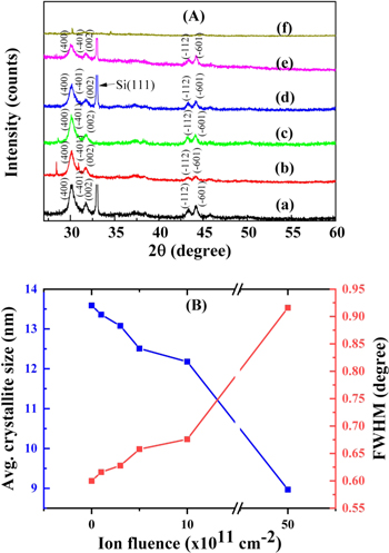
Figure 3. (a) XRD patterns of samples grown on Si substrate and annealed at 900 °C, with different ϕ values of (a) pristine, (b) 1 × 10¹¹ ions-cm−2, (c) 3 × 10¹¹ ions-cm−2, (d) 5 × 10¹¹ ions-cm−2, (e) 1 × 10¹² ions-cm−2, (f) 5 × 10¹² ions-cm−2. (B) Variation of average crystallite size and FWHM with increasing ϕ.
Download figure:
Standard image High-resolution imageThe Debye–Scherrer formula is considered to be an appropriate method to calculate the average crystallite size of a material. However following measures should be kept in mind while using the formula: (i) the reflection width must be free from instrumental effects. (ii) the value of the shape constant K is assumed to be constant but in practice, it is dependent on a number of factors including crystal morphology, sample homogeneity etc. (iii) the deconvolution of the contributions of size and strain/disorder is important in order to obtain rigorous data.28 All the above factors are taken care of while analysing the XRD data. The Debye–Scherrer formula has also been used in previous reports like those from Berencén et al.,29 Ou et al.,30 and Goyal et al.,31 for calculating the average crystallite size in β-Ga2O3 thin films.
It is observed that the diffraction peak intensity and D decrease with the increase of ϕ as shown in Figs. 3a and 3b respectively. The peak almost vanishes at the highest ϕ of 5 × 10¹² ions-cm−2. This indicates a decrease in the crystalline fraction of the film due to ion beam generated defects.32
Figure 4a shows the UV–vis absorption spectra of as-grown and irradiated thin films deposited on quartz substrate. It can be easily seen that nearly all the films have a sharp absorption edge at wavelength ∼240 nm which can be attributed to the strong absorption of photons due to electronic transitions from valence band to conduction band.33 The oscillatory behaviour found in the transmittance spectra of β-Ga2O3 may be due to the interference of reflected wavefronts from the two surfaces of the thin films.34 Ortiz et al.35 also reported the same kind of transmittance spectra for Ga2O3 thin films annealed at 850 °C, deposited on quartz substrate via ultrasonic spray pyrolysis method. Like unirradiated thin films, the irradiated ones also showed high transparency of ∼80% (up to ∼280 nm) except for ϕ = 3 × 10¹¹ ions-cm−2 where it is ∼60%. Although most the thin films are found to be uniform, a natural variance may have caused the lower transmittance at this fluence as other possible causes22,33,36 should affect the transmittance even more pronouncedly at higher ϕ values which was not observed. The energy band gap for β-Ga2O3 thin films is determined from the Tauc's plot37 as shown in Fig. 4b using Tauc's relation.
Where B is a material dependent constant, Eg is the band gap of the material, hν is photon energy and α is absorption coefficient. The value of m depends upon the nature of transition. Here m = 2 is used for direct transition.38 The band gap value of the thin films was obtained by extrapolating the curve on the hν axis. The bandgap remains almost constant within the range 5.10–5.21 eV (see Table I). Almost constant bandgap and transmittance indicate that the defects generated in the thin films by ion irradiation are optically inactive.39
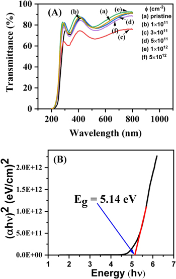
Figure 4. (a) Transmittance spectra of ion irradiated Ga2O3 thin films grown on quartz substrates. (b) Tauc's plot for thin film irradiated with ϕ = 3 × 10¹¹ ions-cm−2.
Download figure:
Standard image High-resolution imageTable I. Values of Eg of β-Ga2O3 thin films irradiated with different values of ϕ.
| ϕ (ions-cm-2) | Eg(eV) |
|---|---|
| Nil | 5.19 ± 0.099 |
| 1 × 10¹¹ | 5.10 ± 0.067 |
| 3 × 10¹¹ | 5.14 ± 0.096 |
| 5 × 10¹¹ | 5.17 ± 0.095 |
| 1 × 10¹² | 5.21 ± 0.096 |
| 5 × 10¹² | 5.11 ± 0.076 |
Figure 5 shows the Raman spectra of as-grown, annealed, and irradiated thin film samples deposited on silicon substrate. The as-grown sample does not show any Raman peak. Thin film annealed at 900 °C shows a small Raman peak at 170 cm−1. This low frequency peak can be assigned to the Ag(2) phonon mode (marked with *) of β-Ga2O3 which comes from the vibration modes by liberation and translation of tetrahedra–octahedra chains in β-Ga2O3.40 An additional peak was observed for transverse optical (TO) phonon mode of silicon substrate41 at 520 cm−1, as shown in Fig. 5. Non-observation of Raman peak for as-grown thin films is due the amorphous nature. As confirmed by XRD measurements, thermal annealing at 900 °C leads to the polycrystalline structure of Ga2O3.
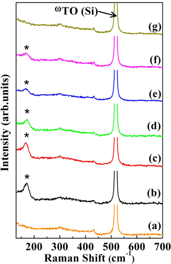
Figure 5. Raman spectra of samples grown on Si substrate; (a) as-grown at RT, (b) annealed at 900 °C (ϕ = 0), (c) ϕ = 1 × 10¹¹ ions-cm−2, (d) ϕ = 3 × 10¹¹ ions-cm−2, (e) ϕ = 5 × 10¹¹ ions-cm−2, (f) ϕ = 1 × 10¹² ions-cm−2, (g) ϕ = 5 × 10¹² ions-cm−2.
Download figure:
Standard image High-resolution imageThe intensity of the β-Ga2O3 Raman peak decreases as ϕ increases. This peak almost diminishes at the highest ϕ. A narrow Raman peak generally indicates high crystalline quality of the samples with fewer structural defects, having large crystalline zones.42 Therefore, Raman measurement confirms that the crystalline fraction of the sample reduces with increase of ϕ which is in accordance with XRD results.
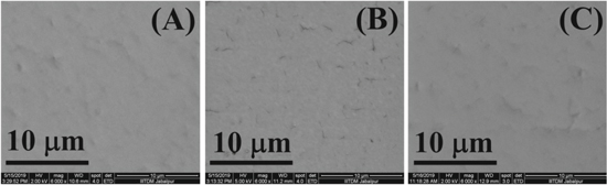
Figure 6 shows the SEM images of the pristine sample (annealed at 900 °C) as well as irradiated samples at different ϕ. The as-grown β-Ga2O3 films show relatively smooth and featureless surfaces without any cracks or pits on the surface. Thereafter, for the irradiated samples from ϕ = 1 × 10¹¹ ions-cm−2 to ϕ = 5 × 10¹² ions-cm−2, a few cracks may be seen on the surface of the samples suggesting no significant change in the surface quality of the samples.
Figure 6. SEM micrographs of (a) pristine sample; and 120 MeV Ag9+ irradiated samples at different ϕ (b) ϕ = 3 × 10¹¹ ions-cm−2 and (c) ϕ = 1 × 10¹² ions-cm−2.
Download figure:
Standard image High-resolution image
Discussion
The grown thin films were found to be slightly O deficient with ratio of Ga to O being 1.43 (rather than 1.50) even after annealing under oxygen environment. Such deficiency of oxygen atoms in β-Ga2O3 thin films may arise due to the formation of O vacancies, Ga-O di-vacancies and neutral O interstitials.43 These types of O deficient β-Ga2O3 thin films are found to be suitable materials for gas sensors at high temperature.44 A similar RBS spectrum was observed by Ortiz et al.35 for β-Ga2O3 thin films deposited via ultrasonic spray pyrolysis method. Berencén et al.29 too reported similar spectra for β-Ga2O3 thin films grown by pulsed laser deposition. The elemental composition of β-Ga2O3 obtained in both the above mentioned reports was in good agreement with our results i.e. 41% and 59% for Ga and O, respectively.
Structural properties of β-Ga2O3 were affected by irradiation of 120 MeV Ag9+ ions. A monotonous decrease in the crystalline quality of the film and that of average crystallite size D was observed with increasing ϕ as confirmed by XRD. Also at the highest fluence i.e. ϕ = 5 × 10¹² ions-cm−2, all the XRD peaks nearly vanish which suggests that further detailed study for ϕ > 5 × 10¹² ions-cm−2 is required to understand if complete amorphization under SHI irradiation can be achieved in polycrystalline β–Ga2O3 thin films. In line with XRD results, Raman spectra of the irradiated thin films also depicted increasing disorder as a function of ϕ of 120 MeV Ag ions. Liu et al.20 also reported the Raman spectra of β-Ga2O3 samples at different ϕ of 25 MeV O ions, and observed a decrease in the intensity of the Raman peak (Ag(2) mode) as ϕ increased due to the increasing disorder of the crystalline material. The decrease in the Raman intensity upon ion irradiation has also been observed in Al2O3, a material that compositionally resembles Ga2O3, and may be expected to show similar behaviour under ion irradiation. Nagabhushana et al.45 reported decrease in intensity of Al2O3 Raman peaks with increasing ϕ of 120 MeV Au9+ ions. The decrease in intensity was attributed to the high defect concentration leading to lattice disorder and internal stress in the crystal structure. SHI irradiation had no noticeable impact on optical properties of β-Ga2O3 as confirmed by UV–vis measurements. This suggests that the SHI induced defects in Ga2O3 thin films may be optically inactive.
The modification of Ga2O3 thin films can be understood by considering the fundamental mechanism of energy loss of an energetic ion as it passes through a material. An energetic ion deposits its energy in a material via two scattering processes, namely, (i) nuclear energy loss (energy loss per unit length given by Sn) caused by elastic interactions with the nuclei of the target atoms, and (ii) electronic energy loss (Se) resulting from inelastic interactions with the electrons.46 At low ion energies, nuclear energy losses dominate over the electronic ones, whereas at ion energies of few MeV per nucleon or above, electronic losses dictate the energy loss mechanism. In the present study, the value of Se (see Fig. 1) for 120 MeV Ag ions in Ga2O3 thin film is ∼25 keV nm−1 and; Sn (∼0.118 keV nm−1) has a significantly lower value. Therefore, the disordering of the Ga2O3 thin films as seen through XRD and Raman measurements should predominantly be caused by large Se deposition. Due to a large bandgap, Ga2O3 shows insulating characteristics unless intentionally doped. Hence, the Coulomb explosion model43 which works based on the creation of a highly ionized region along the ion path, and a violent explosion resulting from electrostatic repulsion in the ionized region, may be responsible for 120 MeV Ag ions induced modification in Ga2O3 thin film. Further explorations are, however, imperative to ascertain the applicability of a theoretical model for ion-beam modifications in Ga2O3 thin film.
In this study, a slight deficiency of oxygen (as suggested by RBS measurements) in the unirradiated polycrystalline thin films may indicate presence of oxygen vacancies. As far as various types of ion beam defects in Ga2O3 thin films are concerned, Liu et al.20 have observed the generation of (VGa + VO)1− divacancies and neutral oxygen interstitial (Oi0) defects, in Ga2O3 single crystal by 25 MeV O ions. Under low–energy ion irradiation (300 keV Ar), Wendler et al.47 have reported formation of point defects at low ϕ and defect clusters at high ϕ in ion implanted bulk β-Ga2O3. Besides, they observed a correlated displacement of atoms implying an incomplete amorphization in Ga2O3. At this point, divacancies, and oxygen interstitials may be speculated as defects created under ion beam. However, a detailed defect analysis is needed to conclude about the nature and type of defects in SHI irradiated Ga2O3 thin films. Similar to observation made in the present study, Tracy et al.14 observed a decrease in XRD peak intensity and reduction in the crystalline fraction of β-Ga2O3 pellets with increasing ϕ of 946 MeV Au ions. However, complete amorphization was not seen even at highest ϕ (1 × 10¹³ ions-cm−2) Although, XRD peaks have almost vanished at ϕ of 5 × 10¹² ions-cm−2 in our study, further experiments and microscopic measurements may ascertain the occurrence of complete amorphization at 5 × 10¹² ions-cm−2 or at a higher ϕ of 120 MeV Ag ions.
Conclusions
Electron beam evaporation of Ga2O3 at RT followed by thermal annealing at 900°C under oxygen flow results in the formation of polycrystalline β-Ga2O3 thin films. It is shown via XRD and Raman spectroscopy that the crystalline quality of the thin films decreases with increasing ϕ of 120 MeV Ag9+ ions. The average crystallite size of β-Ga2O3 also decreases with increasing ϕ. Almost all the samples have transmittance above 80% and cut-off wavelength around 240 nm which makes the prepared thin films suitable candidate for transparent conducting oxide and solar blind photodetector. The bandgap (Eg ∼ 5.14 eV) remained almost constant under ion bombardment as confirmed by UV–visible spectroscopy. The elemental composition of the sample was found to be 41% and 59% for Ga and O, respectively as confirmed by RBS analysis. The SEM micrographs reveal a smooth morphology of the thin films.
Acknowledgments
One of the authors (YSK) is grateful to IUAC, New Delhi for financial support (UFR-62345). The authors are grateful to Abhilash from IUAC target lab for growing thin films. The authors are thankful to G.P. Singh and A. K. Singh for their assistance during sample preparation and RBS measurements, and J. Singh (IUAC, New Delhi) for help during UV–vis. measurements. Support received from Dr. M. K. Roy for SEM measurements is gratefully acknowledged.