Abstract
To enhance the light output of blue InGaN-based light emitting diodes (LEDs), a buried stripe-type n-electrode, expanded stripe-type p-electrode, and reflective p-bonding pad were employed. Flip-chip (FC) LEDs with the expanded p-electrode gave forward voltages of 2.99–3.11 V at 100 mA and series resistances of 3.28–3.94 Ω. The expanded p-electrode FCLED fabricated with 375 nm-thick window and TiO2 adhesion layers produced 22.7% higher light output at 21 A/cm2 than conventional FCLEDs. The expanded p-electrode FCLEDs revealed better current spreading efficiency than the c-FCLED, indicating the importance of the use of an optimised window and TiO2 adhesion layers.
Export citation and abstract BibTeX RIS

This is an open access article distributed under the terms of the Creative Commons Attribution Non-Commercial No Derivatives 4.0 License (CC BY-NC-ND, http://creativecommons.org/licenses/by-nc-nd/4.0/), which permits non-commercial reuse, distribution, and reproduction in any medium, provided the original work is not changed in any way and is properly cited. For permission for commercial reuse, please email: oa@electrochem.org.
InGaN-based light-emitting diodes (LEDs) have attracted a great deal of interest because of their use in various applications, e.g. general illumination and back light unit for display.1 Lateral-geometry LEDs have been generally used for display application. However, lateral LEDs experience some limitations such as low extraction efficiency caused by opaque p-type contact and poor current spreading due to resistive p-GaN.2–4 Furthermore, at high current densities, relatively high-resistance p-type contact and resistive p-GaN cause the Joule heating of LEDs grown on sapphire substrate, which has low thermal conductivity of 0.35 Wcm–1K–1 and so lateral LEDs experience a self-heating problem. The self-heating degrades the light output efficiency and lifetime of the devices and also brings about a shift in the emission spectrum.4 Thus, it is imperative to reduce the thermal resistance of LEDs by adopting efficient device structures and heat sinks.4–6 Flip-chip (FC) packaging technologies have been widely employed to reduce Joule heating,4,5 where highly reflective and low-resistance p-contacts are also used to improve the light extraction and current spreading.6–13 For example, Chitinis et al.,6 investigating self-heating effects at high pump currents in deep ultraviolet (UV) LEDs, found that for deep UV LEDs on sapphire, self-heating was a main cause of early power saturation under dc pumping. It was shown that improvement in heat dissipation by FC packaging consequently increased the dc-saturation currents and hence the output powers. Furthermore, to achieve high light extraction efficiency (LEE) of FCLEDs, the development of high-quality p-type ohmic reflectors with high reflectance, low contact resistance and good thermal stability is essential.7–13 Song et al.,8 investigating the thermal stability of commonly used Ag-based reflectors for blue FCLEDs, showed that the formation of Cu-doped In2O3 (CIO) nano-dots at the Ag and p-GaN interface significantly improved the thermal stability as well as the contact resistivity. In other words, the CIO/Ag reflectors produced a specific contact resistance of 1.28 × 10⁻⁵ Ωcm2 and a reflectance of about 90% at 460 nm when annealed at 530°C for 1 min in air. Lee et al.12 investigated the LEE of bare and encapsulated GaN-based lateral and flip-chip LEDs by means of the Monte Carlo ray tracing method and reported that for the encapsulated LEDs, FCLEDs gave 10% higher LEE than lateral LEDs. Zhou et al.13 investigated the effects of p-type ITO/distributed Bragg reflector and hole-based n-contacts on the output performance of GaN-based FCLEDs. The hole-based n-contacts were formed on the n-GaN by etching via holes through p-GaN and multiple quantum wells (MQWs). The via-hole-based n-contacts were found to effectively improve lateral current spreading, so lessening current crowding. Consequently, the FCLEDs exhibited 15.4% higher external quantum efficiency (EQE) at 90 mA than lateral LEDs. Similar via hole-type n-contacts were used to increase the performance of GaN-based LEDs.14–17 Laubsch et al.15 used a buried n-contact layer under the p-contact, where they were separated by an insulation layer. It was found that the via hole-type n-electrode design enabled a large reduction in the forward bias voltage at high current operation and a considerable enhancement in the LEE. Han et al.,17 investigating the effects of the n-contact design on the electrical, optical and thermal characteristics of thin-film vertical LEDs, reported that as the number of n-contact via holes increased, the forward bias voltages of LEDs (chip size = 1 × 1 mm2) decreased from 3.22 to 3.12 V at 350 mA and their junction temperatures decreased. In this study, a buried n-electrode was also adopted to enhance the light output. However, unlike the previous works, where via-hole type n-contacts and planar p-type reflector were used, a buried stripe-type n-electrodes, via-hole type expanded p-contacts, and Ag-based reflective bonding pads were adopted in this study. In addition, the effects of different window layer thicknesses and adhesion layers on the performance of LEDs were investigated. Simulation was also performed to obtain the optimal thickness of the window layer.
Experimental
InGaN/GaN-based blue LEDs (λ = 450 nm) were grown on (0001) sapphire substrate fabricated by a metallorganic chemical vapordeposition system. The LED structure is composed with a 30 nm-thick GaN nucleation layer, a 3 μm-thick undoped GaN layer, a 2 μm-thick Si-doped n-GaN layer (nd = 5 × 1018 cm−3), active region of seven pairs of InGaN/GaN MQWs, a 0.1 μm-thick Mg-doped AlGaN electron blocking layer (na = 5 × 1017 cm−3), and a 0.2 μm-thick Mg-doped p-GaN layer. Schematic structures of conventional FCLED (referred to here as c-FCLED), buried n-electrode-based FCLED (referred to here as n-buried-FCLED) and n-buried-FCLED with expanded p-electrode (referred to here as p-expanded-FCLED) are illustrated in Fig. 1. An inductively coupled plasma-reactive ion etching (ICP-RIE) system (with Cl2 and Ar gases) was used to etch away p-GaN and MQWs to expose a part of n-GaN. Radio frequency (RF) and ICP powers were kept constant at 200 W and 400 W, respectively. After mesa etching, a SiO2 passivation layer was deposited on the entire top surface of LED chips by plasma-enhanced chemical vapor deposition (PECVD). Then, except the sidewall passivation region, the whole SiO2 was thoroughly removed by a buffer oxide etch solution. For c-FCLEDs, a Ni (3 nm)/Ag (200 nm)/Ni (50 nm) reflective p-electrode was deposited on the p-GaN by an electron-beam evaporator (E-beam). For n-type and p-type metal contacts, a multilayer film of Cr (5 nm)/Al (200 nm)/Ni (50 nm) was deposited on the exposed n-GaN and p-reflector by E-beam, respectively (Fig. 1a). As shown in Figs. 1b and 1c, for the n-buried-FCLED and p-expanded-FCLED, an ICP-RIE was used to remove p-GaN and MQWs to expose and define stripe-shaped n-GaN, followed by a 300 μm-thick SiO2 passivation layer. Then a 40 nm-thick ITO current spreading layer was deposited on the p-GaN region using E-beam, which was annealed at 600°C for 5 min to form p-type ohmic contact. Cr (5 nm)/Al (200 nm)/Ni (50 nm) multilayer films acting as n-type and p-type metal contacts were deposited on the stripe-shaped exposed n-GaN and ITO by E-beam, respectively (Figs. 1b and 1c). For the p-expanded-FCLED, geometrically expanded p-electrodes were used to increase light output power. Then, SiO2 window layers (300 and 375 nm thick) were deposited by PECVD and via holes were formed by etching. Finally, a Ti (3 nm) or TiO2 (3 nm) adhesion layer/Ag (300 nm)/Ti (100 nm)/Al (100 nm)/Ti (100 nm)/Ni (50 nm) reflective bonding pads (both n and p-type) were deposited through the via holes to connect to n- and p-electrodes. These bonding pads serve as not only paths for carrier injection but also reflectors (Figs. 1b–1f). Current-voltage (I–V) characteristics were examined with an Agilent B1505A system to characterize the performance of LEDs (chip size: 1100 × 1100 μm2). In addition, to obtain optimal window layer thickness for the highest reflectance, simulation was performed with FilmWizard computing program made by Scientific Computing International.
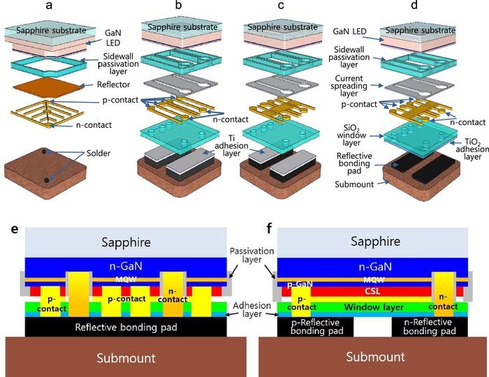
Figure 1. Schematic structures of (a) conventional FCLED, (b) buried n-electrode-based FCLED with a Ti adhesion layer, (c) p-expanded-FCLED with a Ti adhesion layer, and (d) p-expanded-FCLED with a TiO2 adhesion layer. (e) and (f) two orthogonal cross-section diagrams of (d) p-expanded-FCLED with a TiO2 adhesion layer.
Results and Discussion
To maximize the light extraction of FCLEDs, the optimal thickness of the SiO2 window layer was calculated with the FilmWizard computing program. Variation of the reflectance of the window layer/Ag-based bonding pads as a function of thickness is illustrated in Fig. 2. It is shown that the bonding pad with 375 nm-SiO2 gives the higher reflectance of 90.5% at 455 nm than the one with 300 nm-SiO2 (51.1%). The increment in the reflectance is believed to be associated with efficient constructive interference.18 Thus, for comparison purpose, p-expanded-FCLEDs were fabricated using two different thicknesses of the window layers (i.e., 300 and 375 nm). It is shown that Ag only reflector gives higher reflectance compared with the SiO2-based reflectors.
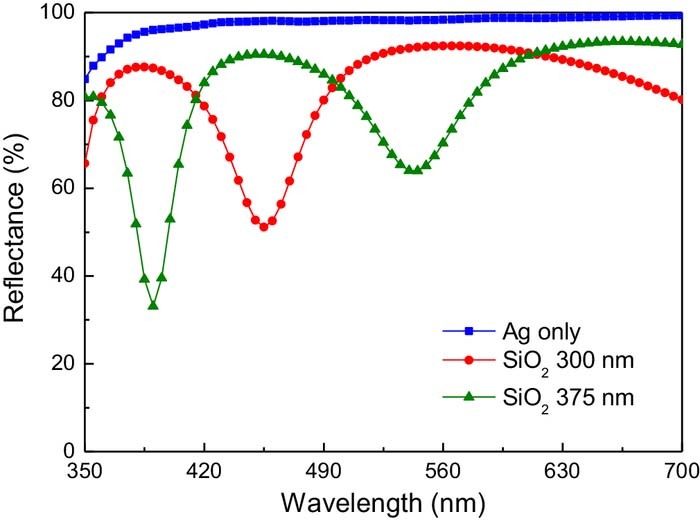
Figure 2. The simulated reflectance of SiO2/Ag layers as a function of SiO2 window layer thickness.
Furthermore, to improve the adhesion of the bonding pad to the window layer, a 3 nm-thick Ti or TiO2 adhesion layers were deposited on the window layer before bonding. Thus, to investigate the effect of the adhesion layers on the reflectance of the bonding pads, the reflectance of the ITO/SiO2/Ti or TiO2/Ag pads (40 nm/375 nm/3 nm/300 nm) was simulated, as shown in Fig. 3. For simplicity, calculations were performed for normal plane wave incidence, assuming that transverse electric (TE) and transverse magnetic (TM) polarizations are equally and randomly mixed. It is shown that across the whole wavelength range of 400–700 nm, the TiO2-based bonding pad gives higher reflectance than the Ti-based pad. For example, at a wavelength of 455 nm, the TiO2-based pad has reflectance of 97.5%, whereas the Ti-based one shows 90.5%.

Figure 3. Calculated reflectance of Ti and TiO2 adhesion layer-based Ag pads.
Figure 4 exhibits the I-V characteristics of different types of FCLEDs (chip size: 1000 × 1000 μm2). It is shown that c-FCLED, n-buried-FCLED, p-expanded-FCLED (300 nm-SiO2), p-expanded-FCLED (375 nm-SiO2), and p-expanded-FCLED (375 nm-SiO2) with a TiO2 adhesion layer give forward voltages of 3.32, 3.12, 3.11, 2.99, and 3.04 V at 100 mA, and series resistances of 5.81, 4.44, 3.94, 3.28, and 3.42 Ω, respectively. The n-buried-FCLEDs reveal better electrical properties than c-FCLEDs since they have better current spreading than c-FCLED. It is also shown that the p-expanded-FCLEDs produce the lower forward voltage and series resistance than c-FCLEDs. This could be due to the increase in the p-electrode area (Figs. 1c and 1d). The inset reveals the leakage characteristics of p-expanded-FCLED (300 nm-SiO2), p-expanded-FCLED (375 nm-SiO2), and p-expanded-FCLED (375 nm-SiO2) with a TiO2 adhesion layer. Note that these FCLEDs give leakage currents lower than 1 × 10⁻⁷ mA at −5 V.
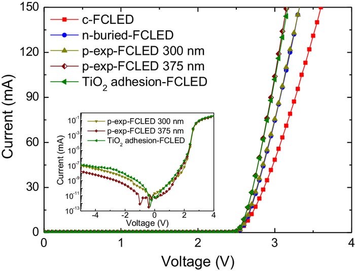
Figure 4. I-V characteristics of LEDs fabricated with different types of structures and electrodes. Inset shows reverse leakage characteristics of the samples.
Figure 5 displays L-I characteristics obtained from different types of blue FCLEDs. For all samples, the light output power increases with increasing drive current up to 100 mA. It is shown that c-FCLED produces higher light output than n-buried-FCLED and p-expanded-FCLED (300 nm-thick SiO2). This is related to the fact that for n-buried-FCLEDs, the p-GaN surface is covered only by two reflective bonding pads but not whole reflector. Note that the p-expanded-FCLED (375 nm-thick SiO2) with the TiO2 adhesion layer yields 22.7% higher light output than c-FCLED at 21 A/cm2. This can be attributed to the fact that the gap between the reflective bonding pads is covered by the expended p-electrode (Fig. 1c) and better current spreading, as shown later. The higher light output in the p-expanded-FCLED (375 nm-thick SiO2) with the TiO2 layer than in the p-expanded-FCLED (375 nm-thick SiO2) with the Ti layer is ascribed to the higher reflectance of TiO2 (Fig. 3). Moreover, the higher light output in the p-expanded-FCLED with 375-nm SiO2 than the one with 300-nm SiO2 is associated with largely enhanced transmittance (Fig. 2). The electroluminescence (EL) spectra in the inset of Fig. 5 exhibit characteristics similar to the trend of the light output power. In other words, the sample with the TiO2 layer produces the highest EL among the samples, while the n-buried FCLED reveals the lowest EL. Considering that current spreading and extraction play an important role in increasing light output power, the improvement would be ascribed to the better current spreading.19 The samples reveal different EL peak energies, depending on the FCLED structures. Such energy differences were previously attributed to the changes in the electric field distribution in the QWs during the EL measurements, which altered the conduction and valance band bending and thereby leading to a shift of the emission energy.20,21 In addition, such a shift was also explained in terms of the inhomogeneous indium composition in the InGaN/GaN MQW at different wafer regions.22

Figure 5. L-I characteristics obtained from LEDs with different types of structures and electrodes. Inset reveals EL spectra of the samples.
Fig. 6 represents IQE curves of different types of blue FCLEDs as a function of current density. The IQEs were measured and calculated using the method reported elsewhere.23 It is shown that all samples undergo IQE droop, although the n-buried- and p-expanded-FCLEDs have better droop behavior than the c-FCLED. For example, the c-FCLED experiences 15.4% drop in the IQE, while that of the p-expanded-FCLEDs are degraded by 6.7 – 6.9%.

Figure 6. IQE curves of different types of blue FCLEDs as a function of current density.
Fig. 7 illustrates relative EQE curves for different types of blue FCLEDs as a function of current. Our samples were grown on 6-inch sapphire wafer, whose thickness is much thicker than those of 2- or 4-inch wafers and packaging requires a full-size wafer. In this study, however, a 6-inch wafer was cut into several pieces for different investigations. Thus, relative EQEs were employed instead of absolute EQEs because of the difficulty in packaging FCLEDs. It is shown that all samples experienced efficiency droop as the current increased to 21 A/cm2. Note that the c-FCLED shows higher efficiency at 21 A/cm2 than n-buried-FCLED and p-expanded-FCLED (300 nm-thick SiO2), but lower efficiency than the p-expanded-FCLED (375 nm-thick SiO2) with the Ti and TiO2 adhesion layers. At 21 A/cm2, the p-expanded-FCLEDs (300 and 375 nm-thick SiO2) produce the higher efficiency than the c-FCLED. For instance, the c-FCLED experiences a 27.4% drop in the EQE, whereas the IQE of the p-expanded-FCLEDs were dropped by 10.4 – 16.1%. It is noteworthy that the EQE characteristics reveal similar tendency to their light output behavior (Fig. 5).

Figure 7. Relative EQE curves of different types of blue FCLEDs as a function of current density.
To examine the current spreading and emission behavior of different types of FCLEDs, the emission images of the LEDs were obtained at a forward bias of 20 mA. The original emission images were reduced to 250 different colors. Fig. 8 displays the plan-view emission images from different types of FRCLEDs. It is noted that for n-buried-FCLED and all p-expanded-FCLEDs, there is a wide band-like contrast in the middle region of the chips, as indicated by the arrows, Figs. 8b–8e. This band corresponds to the gap between the two reflective bonding pads, Figs. 1b–1d. Despite the good current spreading, the uncovered region caused lower output power in the n-buried- FCLEDs than c-FCLED. It is noted that the p-expanded-FCLEDs reveal better current spreading characteristic than the c-FCLED, as shown in Figs. 8a, 8c and 8d. Furthermore, the p-expanded-FCLEDs reveal higher emission than the n-buried-FCLED. A comparison of the IQE and relative EQE implies that the expansion of the p-electrode directly influences the current spreading and light extraction, as confirmed by the emission images. Thus, the optimisation of the window layer thickness and use of a TiO2 adhesion layer are found to be a crucial factor for maximising the light output, as demonstrated in Figs. 5, 7 and 8.
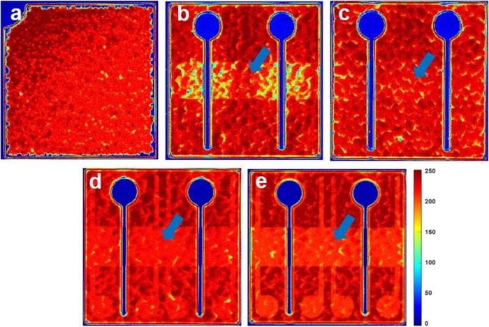
Figure 8. Plan-view emission images from (a) c-FCLED, (b) n-buried FCLED, (c) p-expanded-FCLED (300 nm-SiO2) (d) p-expanded-FCLED (375 nm-SiO2), and (e) p-expanded-FCLED (375 nm-SiO2) with a TiO2 adhesion layer. The arrows denote the gap between the reflective bonding pads.
Conclusions
We investigated how different electrode design structures affected the light output performance of blue InGaN-based FCLEDs and compared their performance with that of c-FCLED. The three new design FCLEDs consisted of p-electrode and buried n-electrode, where two different-thickness SiO2 layers were used to separate the p-electrode from the buried n-electrode and for one sample, the p-electrode was expanded to increase the extraction and current spreading. Further, a Ti (3 nm) or TiO2 (3 nm) adhesion layer was deposited to improve adhesion between the SiO2 window layer and bonding pads. It was shown that the expanded p-electrode-FCLEDs yielded better electrical properties than c-FCLED. Calculation exhibited that the 375 nm-thick SiO2 window layer had higher transmittance at 450 nm than the 300 nm-thick window layer. The light output power of all samples increased with increasing drive current. The expanded p-electrode FCLED with 375 nm-thick window and TiO2 adhesion layers yielded higher light output and EQE than the c-FCLED. The expanded p-electrode FCLEDs exhibited better current spreading efficiency than the c-FCLED. The results show that combination of the buried n-contact and expanded p-contact together with optimized window and adhesion layers can be a promising processing technology for the fabrication of high-performance blue FCLEDs.
Acknowledgments
This work was supported by the Global Research Laboratory (GRL) program through the National Research Foundation (NRF) of Korea funded by the Ministry of Science and ICT (NRF-2017K1A1A2013160).
ORCID
Jong-Ho Kim 0000-0002-9482-6254
Tae-Yeon Seong 0000-0003-0761-3363