
Abstract
The impacts of SiN/Al2O3 bi-layer passivation on the carrier transport characteristics in GaN-based metal-insulator-semiconductor high electron mobility transistors (MISHEMTs) were studied. Various mechanical stresses, as measured by micro-Ramam spectroscopy, were introduced on the GaN channel according to the different passivation systems. The SiN dielectric layer deposited by plasma enhanced chemical vapor deposition on top of the GaN capping layer resulted in compressive stress. On the other hand, the Al2O3 passivation layer deposited by atomic layer deposition on SiN layer generated tensile stress, which compensated the compressive stress produced by the SiN layer. The correlation between the applied mechanical stress induced by the deposited dielectric layers and device performance of the GaN-based HEMT was also investigated. When a slight tensile stress was applied on the GaN channel through the bi-layer passivation, the carrier transfer characteristics were improved in terms of carrier concentration at the AlGaN/GaN interface, as well as carrier mobility and sheet resistance compared to the high compressive stress condition. These results show that the mechanical stress engineering via optimized passivation process is a promising technique for the improvement of the device performance in GaN-based MISHEMTs.
Export citation and abstract BibTeX RIS
GaN-based high electron mobility transistors (HEMTs) have been emerged as a promising device for high-power microwave,1,2 low noise3,4 and high temperature5 applications thanks to its excellent material properties such as wide band-gap, high breakdown voltage, and high sheet carrier densities at the AlGaN/GaN interface. In these GaN-based HEMTs, the role of dielectric layer deposited on top of the AlGaN (or GaN capping) layer is important, as (i) it can effectively reduce gate leakage,6,7 improve current driving8,9 and thereby enhance Ion/Ioff ratio9 of metal-insulator-semiconductor (MIS) HEMTs, and (ii) also suppress current collapse and improve frequency performance10,11 when used as surface passivation. From this point of view, various dielectric materials have been investigated for GaN-based HEMTs including SiO2,12,13 Si3N4,14,15 Al2O3,8,9,16–18 GaO3,19 HfO2,20 Sc2O3,21 ZrO2.22 Al2O3 is one of the most attractive materials due to the high dielectric constant (ɛ ∼ 9.0), band-gap (Eg ∼ 7.0 eV), and breakdown field (∼ 10 mV/cm) despite the fact that threshold voltage (VTH) is instable with Al2O3 dielectric layer used as the device passivation, as well as gate dielectric layer due to the acceptor like trap at Al2O3 interface.23,24
To utilize the advantages of Al2O3 material and prevent the instability of the threshold voltage, a SiN/Al2O3 passivation system was employed, and the related mechanical stress effects were investigated in this work. The impact of mechanical stress generated by the SiN/Al2O3 passivation system on the two-dimensional electron gas (2DEG) transport characteristics was studied in terms of the carrier concentration at the heterogeneous interface and carrier mobility in GaN-based HEMTs.
Device Fabrication
The GaN-based MISHEMTs were fabricated on a sapphire substrate with the epitaxial layer stack of AlN nucleation (100 nm), GaN buffer (1800 nm), unintentionally doped GaN channel (100 nm), AlN interfacial (1 nm), Al0.26Ga0.74N barrier (21 nm) and GaN capping (2 nm) layers grown by metal-organic chemical vapor deposition (MOCVD). The device processing started from the deposition of Ti/Al/Ni/Au (30/100/30/100 nm) followed by rapid thermal annealing for 150 sec at 900°C to form ohmic contacts. Then, phosphorus implantation was conducted for the device isolation. Three different dielectric systems (sample A: SiN 20 nm, sample B: SiN 5 nm/Al2O3 15 nm, sample C: SiN 5 nm/Al2O3 35 nm) were prepared to investigate the mechanical stress effects. A SiN layer was deposited at 250°C using a plasma enhanced chemical vapor deposition (PECVD) system. The process gases for PECVD were SiH4 and N2. An Al2O3 layer was deposited by atomic layer deposition (ALD) using trimethylaluminum (TMA) as a metal precursor and O2 plasma as an oxidant at 150°C. For samples A and B, the net physical thickness of 20 nm was kept the same for the dielectric layer. After opening source and drain contact pads with buffered oxide etch, Ni/Au (30/370 nm) were deposited for gate electrode. The gate length (LG), width (WG), and distance between source and gate (LSG) of the fabricated device were 4.5, 100, and 1 μm, respectively whereas the distance between gate and drain (LGD) was varied from 6.5 to 21.5 μm.
Results and Discussion
To investigate the mechanical stress applied to the GaN, UV-visible micro-Raman spectroscopy measurements were performed as shown in Fig. 1. The in-plane stress was calculated using the equation: Δω = KRσ, where KR = 4.3 cm−1 GPa−1.26,27 Before dielectric layer deposition, the E2-high peak was obtained at 572.3 cm−1. After dielectric layer deposition, the E2-high peak was shifted according to the strength and type of the induced mechanical stress. With increasing SiN thickness, the compressive stress enhances. Therefore, the E2-high peaks were moved to 573.2 cm−1 and 574.2 cm−1 for 5 nm thick SiN layer and sample A, respectively. By contrast, the deposition of Al2O3 layer resulted in tensile stress and compensated the compressive stress caused by the 5 nm thick SiN layer. Thus, the E2-high peak was slightly recovered to 572.8 cm−1 in sample B. In sample C, the tensile stress applied by the 35 nm-thick Al2O3 layer overcomes the compressive stress and consequently, provides tensile stress on the GaN channel, resulting in the shift of E2-high peak to 572.1 cm−1.
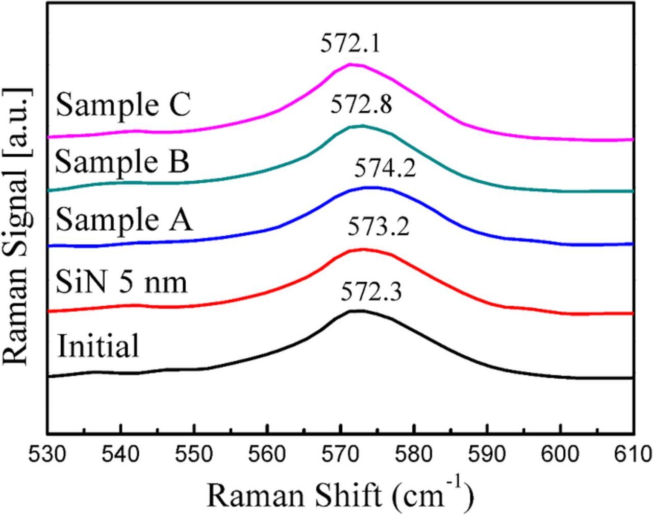
Figure 1. Zoomed-in micro-Raman spectra showing E2-High peaks of AlGaN/GaN HEMTs for initial condition and various passivation systems.
The typical device properties of the GaN-based MISHEMTs were measured to compare the device performance for various passivation systems and corresponding mechanical stresses. Fig. 2a shows the transfer characteristics. The device threshold voltage depends on the thickness of the dielectric layer, reducing VTH with increasing dielectric layer thickness.28,29
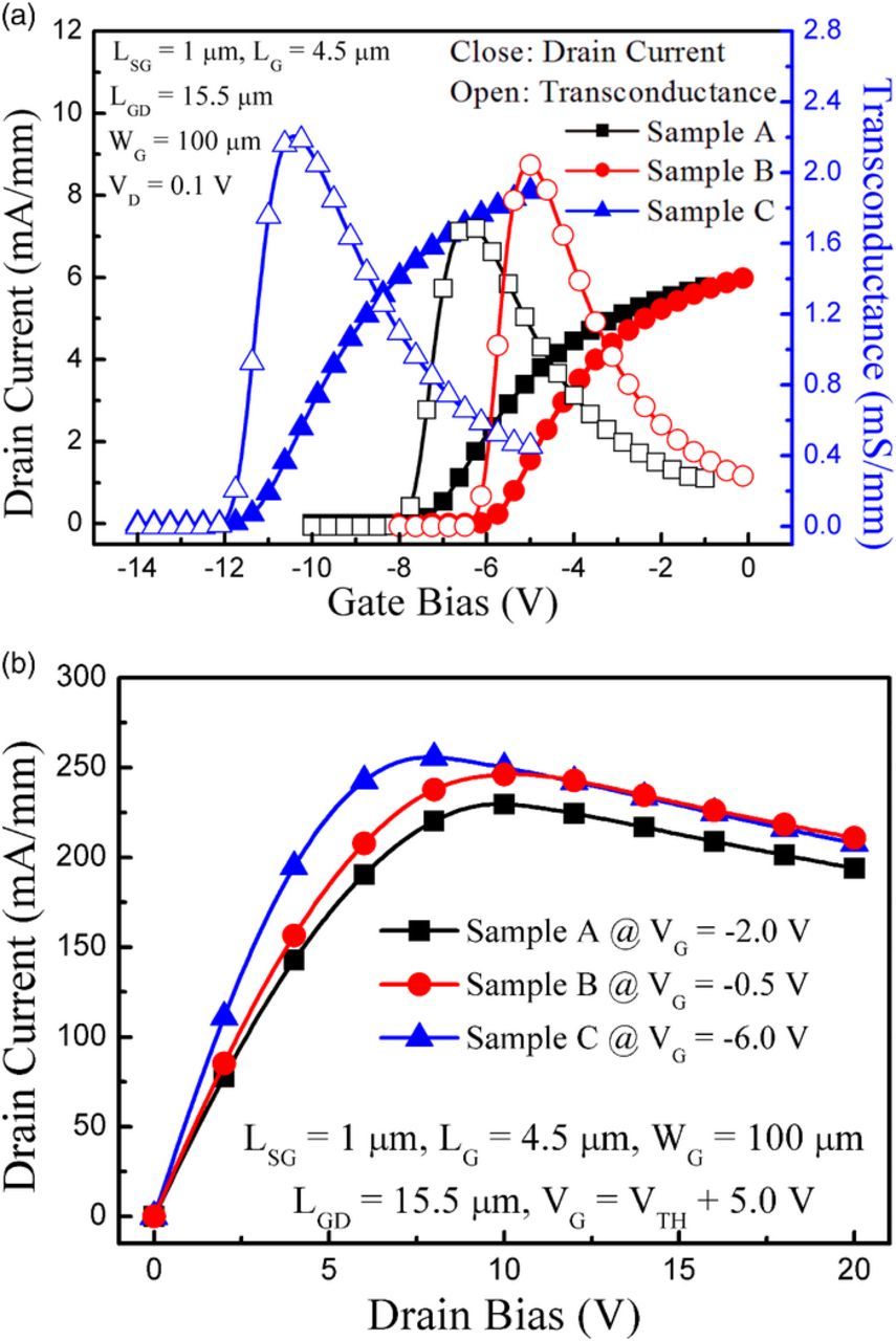
Figure 2. Typical transfer and output characteristics for various passivation systems. (a) Drain current and transconductance as a function of gate bias. (b) Drain current versus drain bias at VG ≈ VTH + 5 V.
We note that the 2DEG concentration also influences the VTH by reducing VTH with increasing 2DEG concentration. However, in our case, the VTH is mainly determined by the dielectric layer thickness. The reason is that in sample B with larger 2DEG concentration compared to that of sample A (discussed in Fig. 4), the VTH is higher than that of sample A since the net electrical thickness of the dielectric layers is thinner because of higher dielectric constant of Al2O3 layer. The VTH of sample C is −11.1 V as it has the thickest net electrical thickness due to the 35 nm thick Al2O3 layer. With reducing compressive stress, the transconductance maximum increases, as well as saturation current obtained at VG = VTH + 5 V. In accordance with the results, device with tensile stress (sample C) shows the best performance among the three samples.
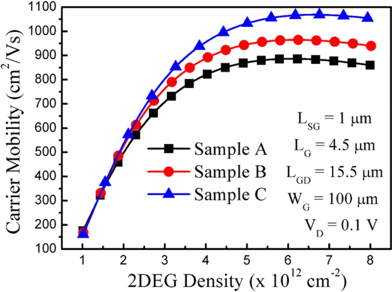
Figure 4. Extracted carrier mobility. Carrier mobility as a function of 2DEG density for various passivation conditions.
The on-resistance (Ron) was extracted from the output characteristics shown in Fig. 2b. The Ron is an important factor which depends on the fundamental carrier transport for a fixed device geometry.25 Ron was extracted from the slope of the linear regime (VD < 5 V) at VG ≈ VTH + 5 V. Compared to the device with compressive stress (sample A), the device with tensile stress exhibits lower Ron (29.7 and 22.4 Ω·mm for samples A and C, respectively.). At higher drain bias (VD > 10 V), the drain current is lower in sample C than in sample B as the thermal emission capability is deteriorated with thicker dielectric layers,30 reinforcing self-heating effects.
To figure out the detailed mechanism for the performance improvement in the device with tensile stress, which presents the best performance, we performed the C(V) measurments and extracted carrier concentrations for various passivation systems at 1 MHz. The capacitance depends on the net electrical thickness of the dielelctric layers; thicker dielectric layer shows lower capacitance. As shown in Fig. 3a, the hysteresis was negligible, reflecting good interface quality between AlGaN/GaN and AlGaN/GaN capping/dielectric layers of the samples.
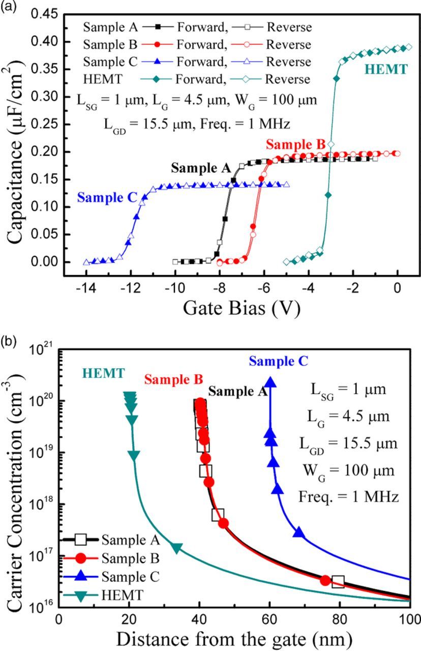
Figure 3. Carrier concentration extraction for various passivation systems. (a) Capacitance as a function of gate bias. (b) Extracted electron concentration versus depth.
The 2DEG concentration (Na) as a function of the corresponding depth (D) in MISHEMTs was extracted8,31 from the C(V) measurement by following equations:
![Equation ([1])](https://content.cld.iop.org/journals/2162-8777/7/6/N86/revision1/d0001.gif)
and
![Equation ([2])](https://content.cld.iop.org/journals/2162-8777/7/6/N86/revision1/d0002.gif)
where, tOX, tCAP, and tBAR are the thickness of dielectric, GaN capping, and AlGaN barrier, respectively. ɛGaN, ɛOX and A are dielectric constants of the GaN and dielectric layer, and area of the gated region, respectively.
![Equation ([3])](https://content.cld.iop.org/journals/2162-8777/7/6/N86/revision1/d0003.gif)
where, CMISHEMT and CHEMT are capacitances of MISHEMT and HEMT, respectively, read from the plateau regions of the C(V) curves. Calculated ɛOX values for the three different samples are provided in Table I. The obtained ɛOX values are comparable with reported values of SiN32 and Al2O38 deposited by PECVD and ALD, respectively. As shown in Fig. 3b, the carrier concentration at hetero-interface enhances with diminishing compressive stress, and the highest carrier concentraion is observed in the device with tensile stress. Piezoelectric field enhances when the compressive stress reduces and tensile stress is applied, improving polarization induced charges,25 which results in enlarged carrier concentraion with reducing compressive stress.
Table I. Summarized GaN-based MISHEMTs characteristics studied in this paper.
| Raman Shift | Stress | VTH | Gm,max | ID @ VG = VTH + 5 V, | RON | Max. Carrier Con. | Max. μ | RSH | ||
|---|---|---|---|---|---|---|---|---|---|---|
| Parameter | (cm−1) | (Mpa/type) | (V) | (mS/mm) | (mA/mm) | (Ω·mm) | ɛOX | (cm−3) | (cm2/Vs) | (Ω/□) |
| Sample A | +1.9 | 456/compressive | −7.1 | 1.7 | 5.5 | 29.7 | 7.74 | 8.8 × 10¹⁹ | 1070 | 608.0 |
| Sample B | +0.5 | 120/compressive | −5.5 | 2.0 | 5.9 | 27.1 | 9.13 | 1.1 × 10²⁰ | 965 | 537.7 |
| Sample C | −0.2 | 48/tensile | −11.1 | 2.2 | 7.5 | 22.4 | 9.89 | 2.1 × 10²⁰ | 890 | 364.7 |
The carrier mobility was also extracted since the carrier mobility is a key parameter which reflects the device performance. For the achievement of the precise carrier mobility (μ) behavior under the gated region, the impact of parasitic resistances (i.e., access and contact resistance) were taken into account using the following equation33,34
![Equation ([4])](https://content.cld.iop.org/journals/2162-8777/7/6/N86/revision1/d0004.gif)
where, Ns is achieved by the integration of the capacitance. WG and LG are gate width and length of the HEMTs, respectively. VD_ADJ is the voltage across the gated region calculated as33,34
![Equation ([5])](https://content.cld.iop.org/journals/2162-8777/7/6/N86/revision1/d0005.gif)
where, RACC and RC are the resistance for access region defined as the distance between gate and source/drain and contact resistance, respectively obtained from Fig. 5.
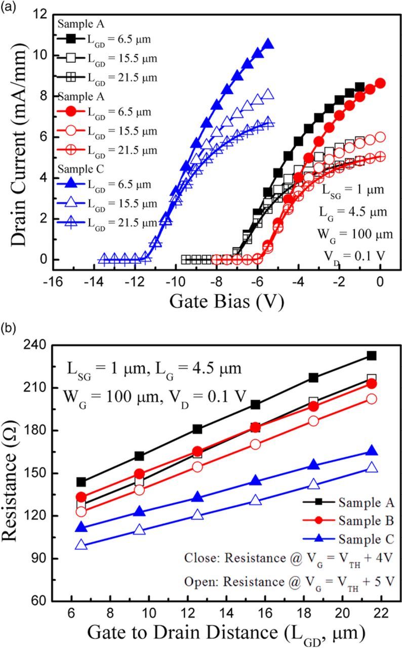
Figure 5. Sheet resistance extraction for various passivation conditions. (a) Drain current as a function of gate bias for various gate to drain distances. (b) Resistance versus gate to drain distance at VG = VTH + 4 V and VTH + 5 V.
As shown in Fig. 4, the maximum carrier mobility increases when the compressive stress reduces, exhibiting the highest carrier mobility in the device with tensile stress (sample C). This phenomenon is different from the conventional Ns - μ tendency35,36 that requires further detailed investigation. Possible scenarios of improvement of the carrier mobility with reducing compressive stress as well as increasing carrier concentration are as follows. First, the conduction-band-edge is significantly varied with reducing compressive stress, generating launcher effect27 and increasing carrier mobility. In addition, when the compressive stress diminishes, the distance between the lattices becomes longer and the mean free path directly related to the scattering time is increased,25 boosting carrier mobility.
To confirm the simultaneous improvement of the carrier concentration and mobility, we have extracted the sheet resistance RSH shown in Fig. 5. In Fig. 5a, ID(VG) curves were measured for various LGD and passivation systems. When the LGD increases, the drain current decreases due to the enlarged access resistance. Therefore, the total resistance linearly increases with increasing LGD as shown in Fig. 5b. The slope of each line yields the RSH and the intercept point with Y-axis indicates the contact resistance.33,34 Compared to the samples A and B, the sample C exhibits dramatic reduction in RSH. This is a clear evidence for the simultaneous improvement of the carrier concentration and mobility in the device with tensile stress because if the carrier mobility is deteriorated with enhancing carrier concentration, the RSH should not result in such a large reduction according to RSH ∼ 1/(Na · μ).36 The device characteristics related to the carrier transfer and device performance are summarized in Table I.
Conclusions
In summary, we have investigated the mechanical stress applied on the GaN channel via the deposition of the SiN/Al2O3 bi-layer passivation and device performance corresponding to the induced mechanical stress. The PECVD-SiN and ALD-Al2O3 results in the compressive and tensile stresses, respectively that compensate each other. The 2DEG transfer characteristics such as the carrier concentration at AlGaN/GaN interface and carrier mobility were improved with decreasing compressive stress, showing the best properties in device with tensile stress. Moreover, when the tensile stress is introduced on GaN channel, the device presents the best performance in terms of the transconductance, saturation current, on-resistance, and sheet resistance. As a result, the mechanical stress engineering through the bi-layer passivation system is an efficient technique for the improvement of the carrier transfer properties and device performance in GaN-based HEMTs.
Acknowledgment
This work was supported by the program of Defense Acquisition Program Administration and Agency for Defense Development.
ORCID
S.-J. Chang 0000-0002-6973-8199
H.-W. Jung 0000-0001-5770-6387