Abstract
There is interest in developing large area Ga2O3 rectifiers for applications in hybrid power converters. Vertical geometry, Schottky rectifiers with area 1.2 × 1.2 mm2 fabricated on thick (8μm), undoped (n = 4.4 × 1015 cm−3) β-Ga2O3 epitaxial layers oN conducting bulk substrates exhibit both high forward current (1A in pulsed mode) and reverse breakdown voltage (VB = 760V). This breakdown voltage was ∼200V higher than rectifiers without the presence of a bilayer SiO2/ SiNx field plate. This edge termination is critical for obtaining high breakdown voltage by reducing electric field crowding around the metal contact periphery. Optimization of the field plate design is still needed, since devices are observed experimentally to breakdown at the contact periphery. When purposely driven to failure at high reverse bias, pits are observed in the high field regions at the edge of the contact. The specific on-resistance (Ron) for these large area rectifiers was 22 mΩ.cm−2, with a figure-of-merit VB2/Ron of 26 MW.cm−2. The potential of Ga2O3 for power electronics is clear when it is realized that these values are still an order of magnitude lower than theoretical values. The diode on-off ratio was in the range 2.7 × 10⁷–2.2 × 10⁹ when switching from +1.5V forward bias to 1–100V reverse bias.
Export citation and abstract BibTeX RIS

This is an open access article distributed under the terms of the Creative Commons Attribution 4.0 License (CC BY, http://creativecommons.org/licenses/by/4.0/), which permits unrestricted reuse of the work in any medium, provided the original work is properly cited.
Wide-bandgap (WBG) devices are promising candidates for next-generation power electronics converters with higher efficiency and higher power conversion densities.1–6 These inverters have applications in a range of power conditioning and control systems, including pulsed power for avionics and electric ships, solid-state drivers for heavy electric motors and in advanced power management and control electronics.1–10 In addition, high-power (∼50kW) is required for fast wireless charging systems in transportation applications.11 Highly efficient energy conversion for these systems is critical and this depends mainly on the ability of power switching transistors to provide low resistance in the on-state and highly resistive off-state conditions. To date, the focus has been on SiC and GaN to provide performance beyond Si.1–5 High cost, challenging fabrication of practical devices, demonstrated reliability, and system integration remain important barriers to the widespread adoption of WBG devices.
A possible solution is hybrid switches, a combination of Si MOSFETs and wide bandgap devices. For example, hybrid modules containing Si MOSFETs and SiC rectifiers are commercially available.12 One component of a switching module is a diode, most commonly Schottky rectifiers. These have fast switching speed, low forward voltage drop and high temperature operability.8–10 Their advantage over p-n diodes is shorter switching times due to absence of minority carriers, but a disadvantage is higher on-state resistance (RON). Employing material with a wider bandgap than Si improves rectifier performance, with lower on-state resistance at a given reverse voltage.1–5 Recently, Ga2O3 vertical geometry rectifiers have shown promising performance in terms of high reverse breakdown voltage (VB> 1kV) and low RON, leading to good power figure-of-merits (VB2/RON).11,13–46 Notable are reverse breakdown voltages (VB) of 2300V for a 150 μm diameter device (area = 1.77 × 10⁻⁴ cm−2)47 and 2440 V breakdown in trench structures.48 Another potential advantage of Ga2O3 are the lower substrate costs compared to SiC.32–42 Reese et al.40 used techno-economic modeling of Ga2O3 wafer cost based on future large-size and high-volume manufacturing scenarios and estimated there could be a >3x cost advantage compared to SiC wafers. This could lead to a significant cost reduction for wide-bandgap power electronics.49–52
In current Ga2O3 rectifiers, breakdown resulting from impact ionization preferentially occurs at the contact periphery unless the electric field is reduced by edge termination.5,27 Baliga's figure of merit (FOM) (ɛrμEbr3) where ɛr is relative dielectric constant and μ is mobility)7,8,42–46 is 4x larger for β-Ga2O3 than SiC and GaN.5–10 The theoretical breakdown field for Ga2O3 is between 5–9 MV/cm, with peak experimental values of 5.3 MV.cm−1.31 Lateral structures have shown breakdown voltages of over 3kV.29 The switching characteristics of Ga2O3 vertical Schottky rectifier show recovery times of 20–30 ns,45,46,48,49,53 faster than Si or SiC diodes.
Vertical geometry, large area planar devices can produce large total forward currents, while maintaining adequate reverse breakdown.45–58 This is a stringent test of material quality, since large diodes increase the probability of incorporating defects into the active region, degrading reverse breakdown voltage.37,39,43,45 Lateral devices can achieve high breakdown voltage using large contact separations, but cannot simultaneously achieve high forward current due to the low total conduction thickness. They also have high on-state resistance.45,48
In this paper, we show vertical geometry Schottky rectifiers with a minimum of process steps can achieve forward currents of 1 A at 2.3 V and reverse breakdown voltages of 760 V for large (0.14 cm2) devices, emphasizing the potential of Ga2O3 for majority carrier switching devices.
Experimental
Epitaxial layers (∼8 μm final thickness) of lightly Si-doped n-type (4.36 × 1015 cm−3) Ga2O3 were grown by Halide Vapor Phase Epitaxy (HVPE) on n+ (3.6 × 1018 cm−3), β-phase Sn-doped Ga2O3 wafers (∼650 μm thick) with (001) surface orientation grown by the edge-defined film-fed method.17,18 The design of the edge termination was guided by device simulations using the MEDICI code of breakdown voltage with various thicknesses, overlap and type of dielectric used in the field plate. The main findings were that the use of an optimized field plate edge termination can increase the reverse breakdown voltage of vertical Ga2O3 rectifiers by up to a factor of two compared to unterminated devices. Moreover, the dielectric material, thickness (and ramp angle if using a bevel edge termination) all influence the resulting VB of the rectifier by determining where the maximum field strength occurs in the device structure. The key aspect in designing the field plate edge termination is to shift the region of the high field region away from the periphery of the rectifying contact. Ar implantation,58 beveling42 or use of trenches48 have also been shown to reduce field crowding in Ga2O3 rectifiers. However, these add complexity to the fabrication relative to simple field plates and in the case of trenches, reduce the current capability.
The rectifiers employed back ohmic contacts (20 nm Ti/80 nm Au) deposited by E-beam evaporation. These contacts were annealed at 550°C for 30 s in N2. The epi surface was treated with ozone for 10 min to remove adventitious carbon contamination, followed by deposition of 40 nm of SiO2 and 360 nm of SiNx by plasma enhanced chemical vapor deposition at 300°C using silane and ammonia precursors. This field plate reduces the maximum electric field around the rectifying contact periphery.1–4,27,55 The SiO2/SiNx contact windows were lithographically patterned and opened with 1:10 buffered oxide etch (BOE) at 25°C. The front Schottky contacts were overlapped 10 μm on the SiO2/SiNx window openings by lift-off of E-beam deposited Ni/Au (120 nm/480 nm). This geometry was guided by the simulations discussed above. The size of these contacts was fixed at 0.12 cm × 0.12 cm. In a few cases, we made smaller diodes and these were found to have higher reverse breakdown (in the range 800–1100V), but their total forward currents were also smaller and in this paper we focused on achieving high numbers for both. Figure 1 shows a schematic of the rectifier. The current-voltage (I-V) and capacitance-voltage (C-V) characteristics were measured in air at 25–150°C on an Agilent 4145B parameter analyzer and 4284A Precision LCR Meter. For reverse voltages >100 V and forward currents >100 mA, a Tektronix 370A curve tracer was used due to the limitation of the Agilent analyzer.
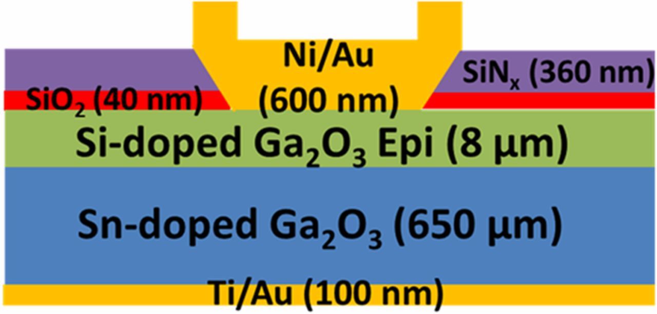
Figure 1. Schematic of vertical β-Ga2O3 Schottky rectifier utilizing a bilayer SiO2/SiNx field plate.
Results and Discussion
Figure 2 shows the C−2_V characteristics used to obtain the drift layer n-type donor concentrations (ND). The value of 4.36 × 1015 cm−3 shows epitaxial layers of β-Ga2O3 can be controllably doped at low enough levels to sustain a large reverse bias while still having good forward characteristics.
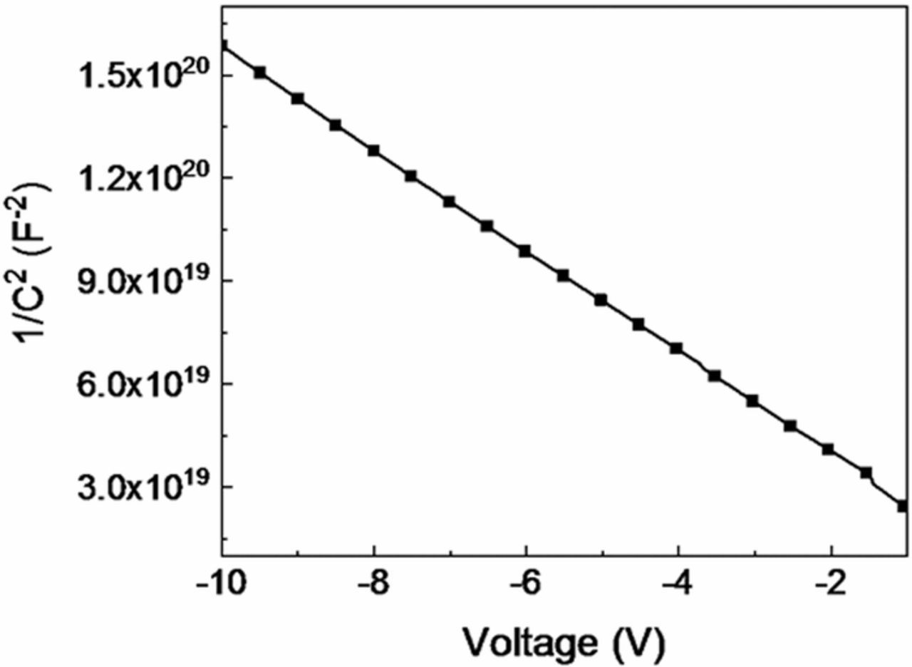
Figure 2. Plot of C−2-V to determine carrier density in drift region.
Figure 3 (top) shows the temperature dependence of forward current (I-V) characteristics. The zero voltage barrier height eΦb0 (e is electronic charge and Φb is barrier height) was determined from the forward current density (J)-voltage-temperature (J-V-T) characteristics by linear fitting of the Richardson's plot (inset of Figure 3). This was 1.04 eV, with a Richardson's constant of 36.44 A.cm−2.K−2, comparable to the values reported23,24 for Pt of 1.15 eV and 55 A.cm−2 K−2. Figure 3 (bottom) shows the temperature dependence of Φb and ideality factor n for 25–125°C. The barrier height decreases with temperature, as expected in pure thermionic emission.55–57 For these lightly doped layers, n should be close to unity, with a small increase due to the image force effect.27 The ideality factor improves with temperature, reaching 1.00 at 150°C, useful for elevated temperature operation.
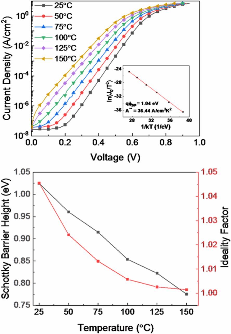
Figure 3. (top) Temperature dependence of forward current. The inset shows the Richardson plot derived from the forward J-V-T data.(bottom) temperature dependence of ɸb and ideality factor.
The single sweep forward current density (J-V) characteristic is shown in Figure 4 (top). The forward current reached 1 A at 2.3 V. In this mode, the collector supply sweeps from 0 V to its preselected value. During the sweep, 1% duty cycle of a 280 μsec pulse width was employed. The on-state resistance was 22.3 mΩ.cm2.
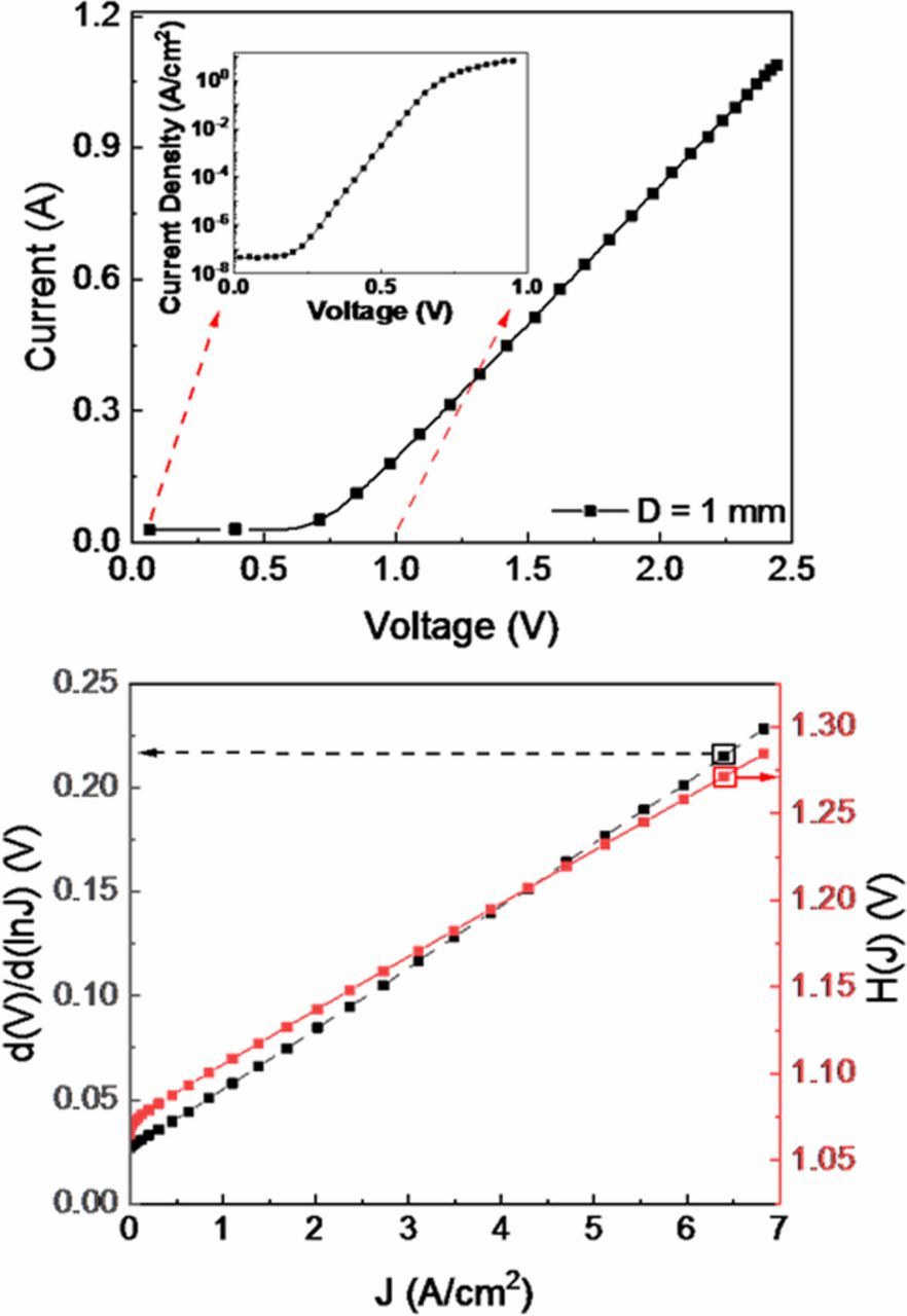
Figure 4. (top) Forward J-V characteristic of rectifier. The inset shows the data on a log scale. (bottom) plot of d(V)/d(ln J) vs J to extract barrier height.
As an independent check on this data, the model of Cheung and Cheung56 was applied to extract Φb, n and series resistance R. Since V = RAJ + nΦB + (nkT/e)ln(J /A**T2), then d (V)/d(lnJ) = RAJ + nkT/e, where A is the rectifier area, A** is Richardson's constant, k is Boltzmann's constant, T is measurement temperature. Thus, a plot of d (V)/d(ln J) vs J will give RA as the slope and nkT/e as the y-axis intercept.56 This data is shown in Figure 4 (bottom).The barrier height is extracted by defining the function H (J) = V - (nkT/e) In(J /A**T2) which is also equal to RAJ+nΦb. Using the n value determined from the plot of d (V)/d(ln J) vs J, a plot of H(J) vs J will also give a straight line with y-axis intercept equal to n Φb. We obtained RON values of 29.2 m Ω.cm2 from the d(V)/d(lnJ) data and 32.4mΩ.cm2 from the H(J) analysis, in agreement with the thermionic emission analysis.
Figure 5 (top) shows the reverse breakdown voltage is 760 V, so the figure of merit (VB2/RON) is 26 MW.cm−2. Rectifiers with much smaller areas (∼10−5 cm2) exhibit higher values of 102–154 MW.cm−2,15,16,24–30 but those devices had lower total forward currents. The 760V breakdown voltage is applicable to efficient power switching in systems for photovoltaic, wind energy and motor drives.11,12,40 Figure 5 (bottom) shows the on/off current ratio was in the range 2.7 × 10⁷–2.2 × 10⁹ when switching from +1.5V forward bias to 1–100V reverse bias. This is better than the previous report,53 due to continued improvement in epitaxial doping control. The reverse recovery time when switching from +2V to −10V, was 33.5 ns, comparable to devices with much smaller rectifier dimensions.14,26,49 More detailed measurements of the diode recovery time to the current level of 25% of the reverse recovery current using a clamped inductive load test circuit showed that for switching from 1A forward current to −300V reverse bias, the recovery time was 64 ns with Irr of 0.82 A, and the dI/dt was 24.7 A/μs.58 These values are comparable to previously reported Ga2O3 trench MOS Schottky diodes, Si-fast recovery diodes (FRDs, Rohm RF1005TF6S) and SiC Schottky barrier diodes from Cree (part number C3D0260A) for turn-off from IF = 1 A.49
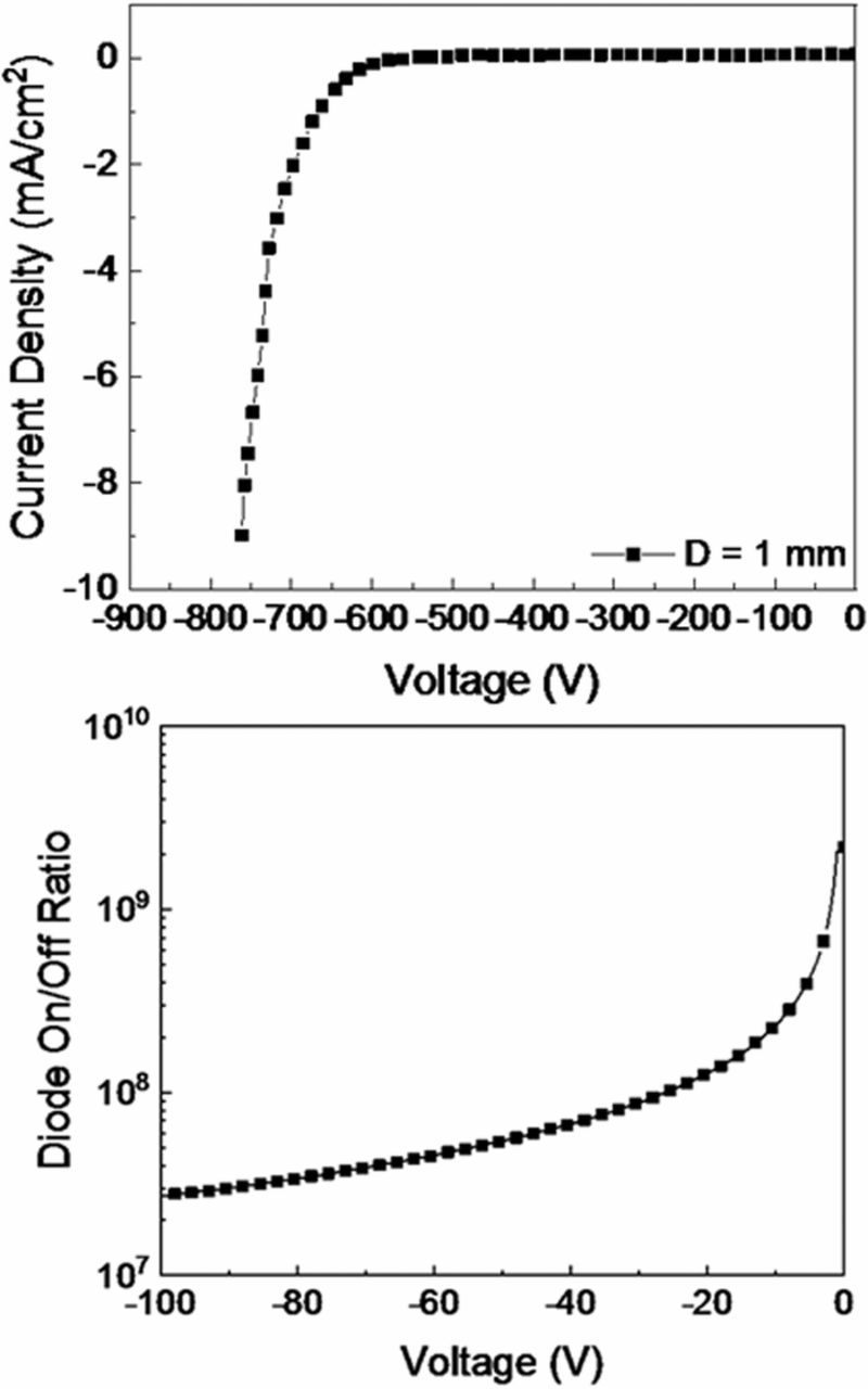
Figure 5. (top) Reverse current density as a function of voltage. (bottom) Rectifier on-off ratio as a function of reverse bias. The on-current was 1 A at 2.3V and the on-off ratio range measured was 3.3 × 10⁹–5.7 × 10⁶.
It is also worth noting the rectifiers when pushed to failure under reverse bias conditions, showed formation of pits along the periphery of the Schottky contact. An example is shown in Figure 7, which shows optical microscope images of the pits formed at the contact edge. The pits are clearer after etch removal of the Au/Ni contact. Figure 8 shows scanning electron microscopy images of these pits, which result from avalanche failure of the Ga2O3 under the high field generated at the edge of the rectifying contact. These results indicate that further optimization of the edge termination material and geometry is needed to reduce field crowding.
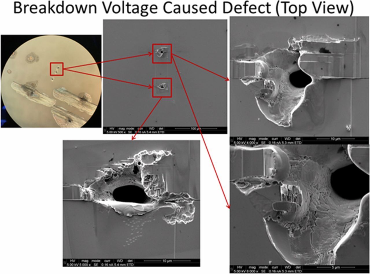
Figure 7. Optial microscope image and close-up SEM images of the pits formed as a result of failure under reverse bias breakdown.
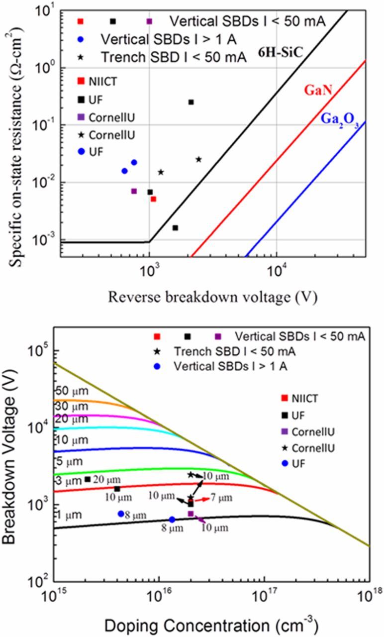
Figure 8. (top) The reverse breakdown voltage of punch-through junctions for Ga2O3 as a function of doping concentration and drift region thickness.(bottom) Specific RON versus VB of state-of-the-art vertical β-Ga2O3 rectifiers.
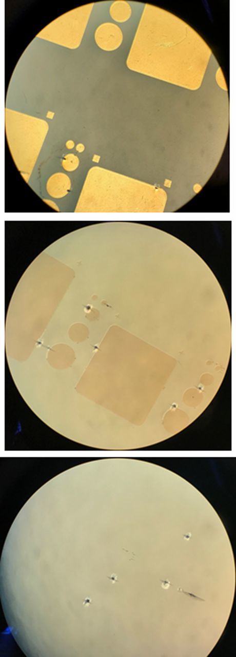
Figure 6. Optical microscope images of rectifiers after reverse breakdown failure. The top image shows the sample with contacts in place, the middle image after Au/Ni etching to remove the contact and the bottom image shows the same area after BOE soaking.
To put our results in context with the previous literature on Ga2O3 and also the performance of SiC and GaN rectifiers, our β-Ga2O3 rectifiers are benchmarked in the plot of specific RON versus Vb in Figure 8 (top). This also shows the relation between breakdown voltage, electric field and doping in vertical geometry rectifier consisting of a lightly doped drift region on a more heavily doped layer on a conducting substrate of these respective materials. Experimental points for Ga2O3 from different groups19,21,22,25–28,34,35,46–48,57 are also shown-these are not yet at the values achieved by the smaller bandgap SiC and GaN, where the theoretical limits are now being approached. Continued development of low defect substrates, optimized epi growth and surface treatments and improved device design and processing methods for Ga2O3 are still required to push the experimental results closer to their theoretical values. Table I also shows a detailed compilation of vertical rectifier results from the literature.
Table I. Summary of vertical geometry Ga2O3 rectifiers reported in literature.
| Reference | Epi Thickness(μm) | Drift Layer Doping (cm−3) | Edge Termination | VB (V) | RON (Ω.cm2) |
|---|---|---|---|---|---|
| Konishi et al.27 | 10 | 1.8 × 10¹⁶ | Yes-field plate | 1076 | 5.1 × 10⁻³ |
| Yang et al.25 | 10 | 4.02 × 10¹⁵ | No | 1600 | 25 × 10−3 |
| Yang et al.26 | 10 | 2 × 10¹⁶ | No | 1016 | 6.7 × 10⁻³ |
| Sasaki et al.21 | Unintentionally doped substrate | 3 × 10¹⁶ | No | 150 | 4.3 × 10⁻³ |
| Li et al.28 | 10 | 2 × 10¹⁶ | Trench | 1350 | 15 × 10−3 |
| Li et al.48 | 10 | 2 × 10¹⁶ | Trench | 2440 | 25 × 10−3 |
| Oh et al.38 | 2 | Undoped, < 3 × 10¹⁶ | No | 210 | 2582 |
| He et al.22 | Unintentionally doped substrate | 2 × 10¹⁴ | No | >40 | 12.5 × 10⁻³ |
| Tadjer et al.34 | ∼10 | 8 × 10¹² | No | 2380 | n/a |
| Fu et al.35 | Sn-doped EFG substrates | 4 × 10¹⁸ | No | low | 0.77 × 10⁻³ |
| Joishi et al.42 | 2 | 2.5 × 10¹⁷ | Bevel | 190 | 3.9 × 10⁻³ |
| Yang et al.46 | 10 | 1.33 × 10¹⁶ | Yes-field plate | 650 | 1.58 × 10⁻² |
| Yang et al.47 | 20 | 2.1 × 10¹⁵ | Yes-field plate | 2300 | 0.25 |
| Yang et al.48 | 7 | 2 × 10¹⁶ | No | 466 | 0.26–5.9 × 10⁻⁴ |
| Li57 | 15, exfoliated | Sn doped | No | 97 | 2.1 × 10⁻³ |
| Gao et al.19 | 10, exfoliated | Sn doped | Ar implantation | 550 | 1.7 × 10⁻³ |
| This work | 8 | 4.4 × 10¹⁵ | Yes-field plate | 760 | 22.2 × 10⁻³ |
Figure 8 (bottom) is a plot of theoretical breakdown voltage of Ga2O3 vertical punchthrough diodes as a function of doping concentration and drift region thickness. This assumes the breakdown voltage is given by VB = ECW-[eNB W2/2ɛɛr], where EC is the critical field for breakdown, W is the depletion depth, NB the doping concentration and ɛr and ɛ the relative and absolute permittivity. Even 3 μm epi layers with doping concentration of 1016 cm−3 should have a theoretical breakdown voltage of ∼1800V. The actual experimental value of VB is well below the theoretical predictions. Our case of 8 μm with doping 4.4 × 1015 cm−3 has a theoretical breakdown more than an order of magnitude larger than the experimental value.43,44
Conclusions
The initial thrust on Ga2O3 electronics is targeted toward high power converters for both DC/DC and DC/AC applications. Schottky barrier diodes on β-Ga2O3 have achieved a breakdown strength of ∼4 MV/cm. The question remains as to whether Ga2O3 will have commercial advantages over the more mature SiC and GaN technology for power switching and power amplifier applications. While the initial device performance looks promising, challenges remain, including growth maturity, thermal limits, cost, and device reliability. The results summarized here show the potential of β-Ga2O3 for fast-switching power devices, capable of simultaneously achieving both high on-state currents and breakdown voltages. The use of thick, lightly doped epitaxial drift regions enable realization of large dimension (0.014 cm2) β-Ga2O3 Schottky rectifiers with large forward current (1A), VBR values of 760 V and power density figures of merit of 26 MW.cm−2. Since power converters require the power device to switch at high frequencies for improved dynamic response capability and reduced passive component size and weight, the performance of these Ga2O3 rectifiers is consistent with these goals. It is likely that Ga2O3 will not displace materials such as SiC and GaN, but possibly supplement them at high voltages in hybrid systems.
Acknowledgments
The project at UF was sponsored by the Department of the Defense, Defense Threat Reduction Agency, HDTRA1-17-1-011, monitored by Jacob Calkins. Research at NRL was supported by the Office of Naval Research, partially under Award Number N00014-15-1-2392. Part of the work at Tamura was supported by "The research and development project for innovation technique of energy conservation" of the New Energy and Industrial Technology Development Organization (NEDO), Japan. Research at Novel Crystal Technology is partially supported by ONR Global (grant # N62909-16-1-2217).
ORCID
Chaker Fares 0000-0001-9596-2381
Fan Ren 0000-0001-9234-019X
S. J. Pearton 0000-0001-6498-1256
Marko Tadjer 0000-0002-2388-2937