
Abstract
In this work, we have compared and modeled the electrical characteristics of two different geometrical structures of unintentionally doped (UID) thin film β-Ga2O3 based Schottky barrier diodes (SBD). It was observed that a lateral SBD structure can withstand much higher breakdown voltage compared to the vertical SBD structure, but suffers from significantly higher on-resistance, which can be explained considering the differences in their geometrical configuration. The schottky barrier height was determined from both capacitance voltage (C-V) and current density voltage (J-V) characteristics of the SBDs, which matched well among themselves and with the values reported in the literature. The C-V measurement was also used to determine the doping concentration in the β-Ga2O3 substrate, which agreed well with the manufacturer specifications.
Export citation and abstract BibTeX RIS
More efficient power electronics are on high-demand in the power electronics industry to reduce energy costs and ensure stable energy supplies. Because silicon based power devices are reaching their operational limits, researchers are continuously looking for new materials capable of enduring higher operating voltages and currents. Wide bandgap (WBG) materials are the best candidates due to their high breakdown voltages and low on-resistances, which lead to a lowering of power-switching losses.1 The power devices based on WBG semiconductors can also be operated at higher temperatures than their silicon counterparts due to reduced thermal generation because of their wide bandgap and typically higher thermal conductivities.2,3 Thus, WBG semiconductors, such as GaN and SiC have received considerable interest in realizing high power diodes and transistors over the last couple of decades. However, these materials still face a number of challenges including material reliability that affects high voltage operation and causes high cost impeding mass production.4,5 While single crystal silicon substrates can be grown from the melt using standard crystal growth techniques, in large sizes and with extremely high crystal quality, SiC and GaN substrates cannot be grown from the melt, which, in turn, dramatically increases their cost. Additionally, SiC substrates have defects that propagate through epitaxial SiC layers as well as GaN, which is grown on non-native substrates such as Sapphire, SiC or Si, and severely limit the power handling capabilities of power devices and their reliability.
Ga2O3 is an emerging WBG semiconductor with excellent promise in realizing power electronic devices.6,7 Its bandgap (4.8–5.1 eV) is significantly larger than those of SiC and GaN, allowing it to handle much larger electric fields and producing substantially high Baliga Figure-of-Merit (FOM) for power devices; almost 4–10 times larger than that of SiC or GaN.8,9 In addition, unlike GaN and SiC, single crystal Ga2O3 can be grown by standard melt growth methods that are favorable for standard mass production of power devices. One known issue of Ga2O3 is the lack of p-type doping, which although limits the range of realizable power devices, still makes a great number of single carrier type devices possible, as it has been recently demonstrated in Ga2O3 based Schottky barrier diodes (SBD),10–12 metal-oxide-semiconductor field effect transistors (MOSFET),13 metal-semiconductor field effect transistors (MESFET),14 and high-electron-mobility transistors (HEMT).14,15 Green et al. obtained breakdown field up to 3.8 MV/cm with Ga2O3-based MOSFET which is even higher than those of SiC (3.5 MV/cm) and GaN (3.3 MV/cm) theoretical breakdown values.16–18 Exceptional results have also been obtained from several vertical geometry β-Ga2O3 SBDs with breakdown voltages exceeding 1 kV.19,20 The vertical Ga2O3 based Schottky diode by Yang et al. showed a breakdown voltage of 1076 V with excellent Schottky characteristic exhibiting near unity value (1.03) ideality factor obtained at room temperature as well as at 200°C.
In contrast with vertical schottky diodes, the lateral ones offer a planar geometry that can be batch fabricated easily and be completely isolated from one another. Additionally, since only the epitaxial layer is important for device operation, the device layer structure can be thin and can be realized on thin flexible substrates leading to much faster heat removal through the substrate, while also offering low cost of materials. Very recently, exfoliated β-Ga2O3 nanomembranes, which were previously used in field effect transistors (FETs) as a channel material,21 have been used to fabricate lateral type SBD.22 The resulting breakdown voltage was enhanced to a record breaking 3 kV with the use of a field plate,23,24 which is much larger than that reported for the non-field-plated β-Ga2O3 nanomembrane channel based SBD.22 Unfortunately, the mechanically exfoliated β-Ga2O3 nanomembranes were deposited through a solvent based transfer process, which makes their mass production challenging. On the other hand, epitaxially grown β-Ga2O3 thin film based lateral structure SBDs have remained relatively unexplored. In 2016, Zhang et al.25 investigated a single crystal β-Ga2O3 lateral structured SBD to analyze the deep level defects in the bandgap of β-Ga2O3. In 2014, Splith et al.26 investigated the Cu Schottky contact on a heteroepitaxial layer of β-Ga2O3 utilizing a lateral structure. However, none of these groups explored the reverse bias characteristics of the SBD beyond −3 V or breakdown in these devices.27 In this article, for the first time, we have systematically investigated a lateral type β-Ga2O3 thin film based SBD with breakdown voltage exceeding −100 V, and compared with a vertical type β-Ga2O3 SBD fabricated from the same wafer, side by side. The lateral SBD demonstrated much higher breakdown voltage than the vertical one, but had much larger on-resistance. The schottky barrier height for the Ni/Au contact was determined from C-V and I-V measurements, which was found to agree quite well with previously reported values.
Experimental
The substrate used in this work for SBD fabrication is a Si-doped (100) 6° off-cut β-Ga2O3 grown at Leibniz Institute of Crystal Growth (IKZ) by Czochralski method with donor concentration (ND) 2–3 × 1017 cm−3. The substrate is ∼450 μm thick and the epitaxial layer has a thickness of ∼290 nm, which is unintentionally doped with Si during the growth process. The samples were cleaned following a conventional cleaning method; first with acetone and isopropyl alcohol to degrease the samples and then by deionized water. To fabricate the lateral Schottky diodes, Plasma Enhanced Chemical Vapor Deposited (PECVD) silicon oxide was used as the masking layer to selectively etch the top UID layer for the annular ohmic contact formation. The inductively coupled plasma etching of UID layer was carried out using 20 sccm of BCl3 gas flow, with source and bias powers of 200 watts and 32 watts respectively.28 This was followed by electron-beam evaporation of titanium (50 nm)/gold (300 nm) (Ti/Au)29,30 to form the ohmic contact with the substrate, followed by rapid thermal annealing in the presence of N2 at 450°C for 1 min.31 Finally, a circular nickel (20 nm)/gold (150 nm) Schottky contact was deposited, using E-beam evaporation.32 Figures 1a and 1b show the schematic diagrams of vertical and lateral Ga2O3 Schottky diodes, respectively.
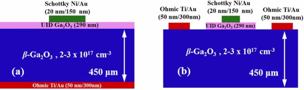
Figure 1. Schematic drawing of (a) a vertical Schottky diode, and (b) a lateral Schottky diode with Schottky contact formed on unintentionally doped (UID) β-Ga2O3 thin film layer.
Figures 2a and 2b show the optical images of the vertical and lateral device structures corresponding to the schematics in Figures 1a and 1b. For lateral SBD, the diameter of the Schottky metal contact on the 290 nm epilayer is 100 μm, which is similar to the dimensions of Ga2O3 devices reported in the literature, where the diameter typically ranges from 100 to 300 μm.10,33–36 The unetched circular UID layer and the annular ohmic contact of the lateral structure have diameters of 120 and 360 μm respectively. The Schottky contact of the vertical SBD is slightly bigger than that of the lateral SBD in this work, with a diameter of 210 μm but is within the typical range of dimensions found by other groups.20,33,36,37
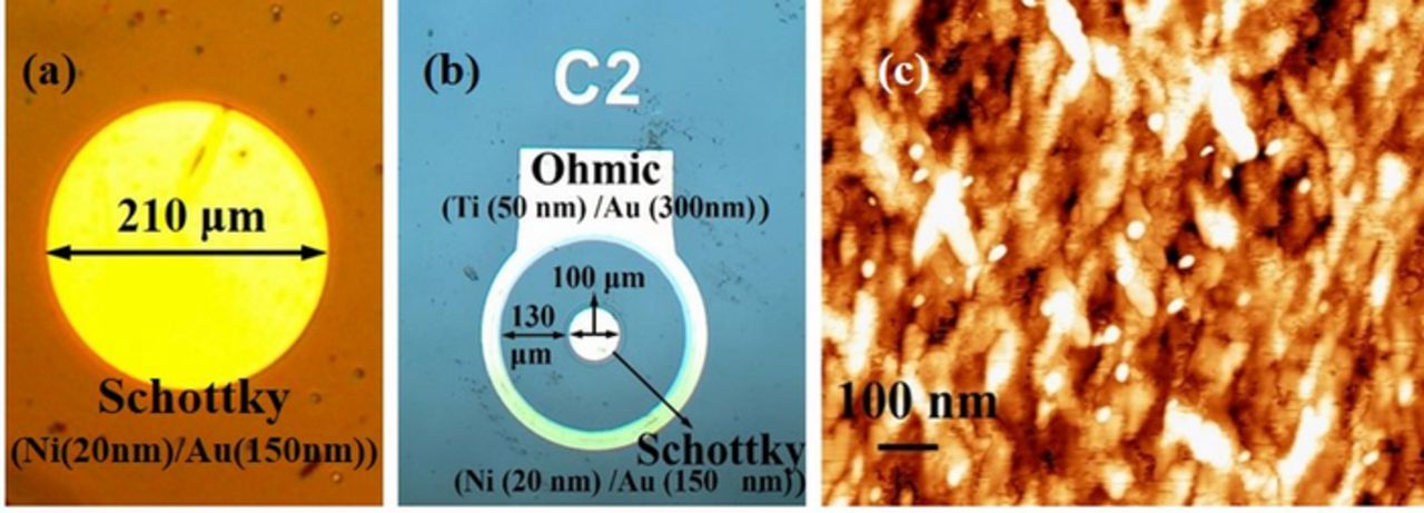
Figure 2. (a) Optical image (top view) of a vertical diode, showing the diameter of the Schottky contact to be 210 μm. (b) Optical image (top view) of a lateral diode showing the annular ohmic contact and a circular Schottky contact in the middle. The gap between the Schottky and Ohmic contact is ∼130 μm, while the Schottky contact diameter is 100 μm. (c) AFM image of bare β-Ga2O3 sample. The rms roughness is ∼ 1.3 nm. The horizontal scale bar (as shown in the figure) is 100 nm. The vertical scale bar (not shown in the figure) is 9.36 nm.
Figure 2c shows the atomic force microscope (AFM) image of the UID surface of the Ga2O3 sample exhibiting a topography with rms roughness of 1.4 nm. Several irregular and uneven features can be seen, which gave rise to a much higher rms roughness than expected in these layers as reported in other works (typically ∼0.3 nm35,38,39), indicating significant material quality issues (including uneven film thickness and presence of polycrystalline domains) in the epitaxial layer. However, the rms roughness taken at a different area of the sample that does not have uneven features was found to be 0.3 nm, which is consistent with the values in the literature.33,38–41
Results and Discussion
Figure 3a shows the forward bias (0 to 2V) characteristics of the annular (lateral) diode structure in semi-log scale clearly exhibiting a ∼5 orders of magnitude change in the forward current value, while Fig. 3b shows the current density (J) vs. voltage (V) curve in reverse bias of the same diode in semi-log scales. The J-V plot in Fig. 3b demonstrates a very good switch characteristics with a high breakdown voltage (−80 V, defined as the sudden rise in current under reverse bias reaching a magnitude more than 10 times the average value at low reverse bias), and reveals that the reverse bias current slowly increases from 10−3 to 10−2 mA/cm2 with increasing reverse bias, before finally beginning to rise sharply beyond −80 V (inset of Fig. 3b). Taking the reverse bias current value of 3 × 10⁻³ mA/cm2 (valid over the reverse bias range of 0 to −20 V) as IOFF (Fig. 3b log scale) and, the forward bias current value at 2 V as ION = 490 mA/cm−2 (Fig. 3a) the ION/IOFF value can be computed to be ∼1.63 × 10⁵, which is very comparable to the Ga2O3 devices reported by other groups.40,42 The ON/OFF ratio is a significant metric for a SBD that is often used as a predictor of its switching performance. This indicates that the diode performance is quite good although the material quality may have resulted in the high contact and semiconductor resistances. Fig. 3c shows the forward bias (0 to 2V) characteristics of the vertical SBD structure in semi-log scale, revealing a ∼4 orders of magnitude change in the forward current. Fig. 3d shows the J-V curves of the same structure in semi-log scale, indicating the reverse breakdown voltage for the vertical structure, although not shown (few of these devices, especially those with large reverse current, sometimes did not recover from breakdown. So, this device was not pushed to breakdown), is typically only a few volts. The on-resistances (RON) were estimated from the slopes of the linear region of the J-V plots and were calculated to be 1260 mΩ.cm2 and 85 mΩ.cm2 for lateral and vertical devices, respectively. These values are much higher than those reported in Ga2O3 schottky barrier diodes (SBD), which can go down to a few mΩ.cm2.20,33,37. Such large deviation can again be attributed to the material quality of the Ga2O3 layers. To investigate any influence of schottky contact diameter on the VBR of vertical diodes (fabricated on another substrate), the VBR values for three vertical SBDs with different sizes of schottky contacts (diameters of 100, 150 and 300 μm) were measured, and are shown as the inset of Fig. 3d. VBR values remained relatively unchanged with the diameters of the schottky contacts, which substantiates that the difference in reverse bias voltage between the lateral and vertical devices (where the lateral device has a smaller diameter than the vertical device) is not significantly affected by the difference in their size.
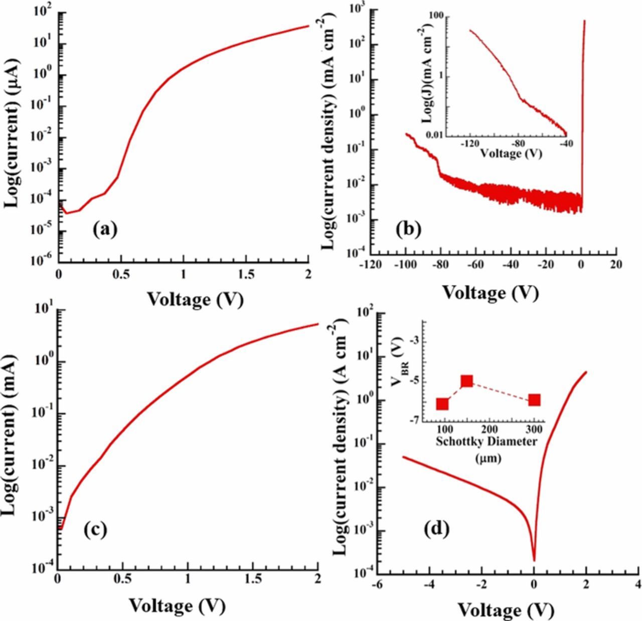
Figure 3. (a) Current vs. voltage (I-V) plot of a lateral geometry Schottky barrier diode in forward bias region in semi-log scale. (b) J-V plot of the same device plotted in semilog scale. Inset shows exponential rise in current beyond −80 V, which is considered as the breakdown voltage. (c) Current vs. voltage (I-V) plot of a vertical geometry Schottky barrier diode in forward bias region in semi-log scale. (d) J-V of the vertical device plotted in semilog scale showing continuous increase in current from which VBR < −5 V is estimated. Inset shows breakdown voltage for vertical diodes plotted against Schottky contact diameter.
To explain the differences in VBR and RON values between vertical and lateral SBDs, the current flow path in these two device structures has been considered. In lateral devices, under forward bias, current is expected to flow mostly laterally, confined to a small depth near the surface, over a distance of ∼130 μm, which is the distance between the ohmic and schottky contacts in the lateral device (see Fig. 2b). In reverse bias, the reverse bias voltage is expected to drop across this same path length. The conductive path for the lateral SBD is shown schematically in Fig. 4a. On the other hand, the conductance path for the vertical devices mostly consists of a vertical cylinder through the UID, which offers most of the resistance, and a more conical structure in the conductive substrate of much smaller resistance. In reverse bias, the voltage will be mostly dropped across the UID layer, which will determine the reverse bias breakdown voltage. The conductive path for the vertical SBD is shown schematically in Fig. 4b. Comparing the two structures in Figs. 4a and 4b, it is evident that the long conduction path through the highly resistive UID layer of ∼130 μm length between the Schottky and the Ohmic contact, is expected to result in a much higher on-resistance for the lateral SBD compared to the vertical one that has only about 0.3 μm of UID path. On the other hand, the same longer path, under reverse bias can reduce the peak electric field very significantly in the lateral SBD compared to the vertical one, thus resulting in much higher breakdown voltage in the former. It should however be noted that the current crowding phenomenon at the corners of the UID layer in the lateral diode structure, can lead to a spike in the electric field at the edges of the schottky contact (as shown in Fig. 4a), which can lead to a reduction in the expected breakdown voltage. Nonetheless, the trends in reverse breakdown voltage and on-resistance should be generally valid and were also observed experimentally. The breakdown field in the vertical SBD can be calculated considering the reverse breakdown voltage of at least −6 V dropping across the 0.29 μm UID Ga2O3, which yields a breakdown field of ∼2 × 10⁵ V/cm, which is an order of magnitude smaller than the breakdown field of β-Ga2O3 with a value of 8 × 10⁶ V/cm.20,34,43 This could again be related to the poor material quality of the Ga2O3 layers.

Figure 4. (a) Electric field lines under reverse bias for the lateral Schottky diode structure. The field lines are lateral between the Ohmic and the Schottky contacts, mostly confined to a small depth from the surface. Current crowding is expected at the edges of the Schottky metal contact. (b) Electric field lines under reverse bias for the vertical diode structure.
The Schottky barrier height between the Ti-Au schottky contact and β-Ga2O3 was estimated by both Capacitance-Voltage (C-V) and the J-V characteristics. The capacitance voltage relationship for Schottky barrier is given by  ,44,45 where A is the Schottky contact area, V is the applied voltage, Nd is the ionized donor state, ɛs is the dielectric constant of β-Ga2O3 and Vbi_cv is the built-in potential. The experimentally measured values of 1/C2 are plotted against the applied voltage V in Fig. 5a from which, the built-in potential Vbi_cv is determined from the x-intercept V0 using the relationship V0 = Vbi_cv–kT/q.10,46 The value of V0 comes out to be ∼1.15 eV from Figure 5a, and thus, Vbi_cv turns out to be ∼1.176 V at room temperature. The built-in voltage can also be approximately determined from the J-V characteristics of the diodes by extrapolating the forward bias current density J to zero and by noting the x-axis intercept.10,46,47 The intercept value for both the lateral and vertical SBDs can be found from Fig. 5b and its inset to be ∼1.15 V. This estimate matches very well with that from the C-V measurements. The Schottky barrier height (SBH) can be determined from the relationship, Φb = qVbi + (EC − EF). Assuming the effective mass of electron (m*) to be 0.34m0, the (EC − EF) value has been reported by several groups to be ∼0.1 eV,12,48,49 which makes the SBH on these diodes ∼1.25 eV, which matches very well with the values reported in the literature for Ni schottky contact on (100) β-Ga2O3.50,51 It should also be mentioned that the SBH of schottky contact on (010) β- Ga2O3 has generally been observed to be ∼1.55 eV, irrespective of the schottky contact metal (i.e. Ni, Pd, or Pt),12,49 which is ∼0.3 eV higher compared to (100) and (̅201) β- Ga2O3, and has been attributed to possible surface Fermi level pinning in the (010) layer.12,49
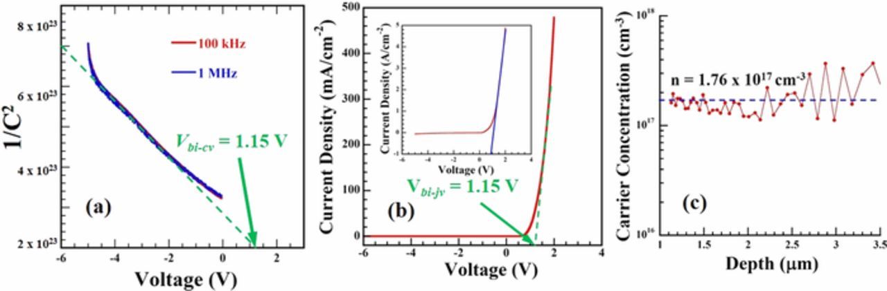
Figure 5. (a) 1/C2 Vs. Voltage plot from C-V measurement of lateral Schottky diode. The X intercept represents the built-in potential. From the Figure, the built-in potential is ∼1.15 V. (b) Built-in voltage approximation from J-V curve of lateral Schottky diode. Vbi-jv for a Schottky diode is ∼1.15 V. Inset shows the built-in potential approximation using J-V curve for a vertical schottky diode. (c) Doping profile of the Ga2O3 structure as derived from the C-V analysis. The uniform doping concentration is n = 1.76 × 1017 cm−3.
The C-V method also yields the free carrier density as a function of depth from the relations:52
![Equation ([1])](https://content.cld.iop.org/journals/2162-8777/8/6/Q106/revision1/d0001.gif)
where C is the measured capacitance per unit area. Equation 1 was used to determine the carrier density nCV as a function of zCV by eliminating C, and the corresponding plot is shown in Fig. 5c. Carrier concentration only up to z = 3.5 μm is shown in the figure, as it becomes very noisy afterwards, where the capacitance became too small to be measured accurately. From Fig. 5c carrier density is found to be varying around an average value of ∼1.76 × 1017 cm−3 although with larger depth it became quite noisy. Nonetheless, the average value agrees very well with the value provided by the wafer manufacturer (2–3 × 1017 cm−3) as discussed before.
Conclusions
In summary, we have investigated and compared the electrical characteristics of both lateral and vertical geometry β-Ga2O3 thin film based SBDs for the first time, to the best of our knowledge. A significantly higher breakdown voltage as well as on-resistance was demonstrated by the lateral SBD compared to the vertical SBD, which can be explained by the difference in device geometries. The J-V characteristics, which demonstrated a high ON-OFF ratio, as well as C-V measurements, were used to estimate the SBH, which agrees well with earlier reports.
Acknowledgment
We acknowledge the financial support for this work by a NASA SBIR grant (NASA Award No. NNX17CG70P) through Structured Materials Industries, Inc. and the National Science Foundation Grants# IIP-1602006 and ECCS-1809891.
ORCID
Digangana Khan 0000-0002-3239-5129