Abstract
Five-layer crystalline thin film structures were formed, consisting of ZrO2 and Co3O4 alternately grown on Si(100) substrates by atomic layer deposition at 300°C using ZrCl4 and Co(acac)3 as the metal precursors and ozone as the oxygen precursor. The performance of the laminate films was dependent on the relative content of constituent oxide layers. The magnetization in these films was nonlinear, saturative, and with very weak coercive fields. Electrical measurements revealed the formation of significant polarization versus external field loops and implied some tendency toward memristive behavior.
Export citation and abstract BibTeX RIS

This is an open access article distributed under the terms of the Creative Commons Attribution 4.0 License (CC BY, http://creativecommons.org/licenses/by/4.0/), which permits unrestricted reuse of the work in any medium, provided the original work is properly cited.
Co3O4 and ZrO2 thin films and their nanolaminates are of interest as functional thin films possessing advanced electronic, optical, magnetic and mechanical properties, making these materials attractive for several applications.
ZrO2 can be used in gas sensors,1,2 catalytic supports,3,4 thermal barrier coatings,5,6 buffer layers for superconductors7,8 and as dielectric material in dynamic random access memory (DRAM)9–13 and resistive random access memory (RRAM) devices.14,15
Co3O4 has been investigated as a gas sensor,16,17 catalyst,18,19 anode material for lithium-ion batteries,20 supercapacitor electrode,21 superhydrophobic coating,22,23 and magnetic semiconductor.24 Co3O4 has also demonstrated resistive switching properties, which are important regarding its potential applications in RRAM devices.25,26
Co3O4 and ZrO2 oxides may be grown using different physical and chemical techniques, such as solution spray pyrolysis,27–29 chemical vapor deposition,30–33 pulsed laser deposition,34,35 sol-gel,36,37 electron-beam evaporation,38,39 or, atomic layer deposition (ALD).40–46 Herewith, ALD may be regarded as the ultimate method providing the most precise thickness control over large substrate areas.
ZrO2 has been used in nanolaminates as one alternating component together with, e.g., Al2O3,47–50 SiO2,51 Ta2O5,52,53 HfO2,53,54 Er2O3,55 Gd2O3,56 and Y2O3.57 Studies on nanolaminates or multilayered structures containing Co3O4 as one of the constituents58,59 as well as ALD-grown nanolaminates containing both Co3O4 and ZrO259 have so far been quite scarce. In the earlier study devoted to ZrO2-Co3O4 nanocomposites grown by ALD using the same chemistry based on cobalt acetylacetonate, zirconium tetrachloride and ozone,59 the deposition process for cobalt oxide was investigated and established, determining suitable evaporation temperature for Co(acac)3 precursor, as well as by recording linear relationship between growing mass and the amount of deposition cycles. Using the suitable deposition parameters, ALD growth of ZrO2/Co3O4 double layers was demonstrated, together with their performance as dielectric and magnetic materials.
In connection with the demand for materials, which could be applied in novel memories because of their advanced magnetic and electric properties, this study was devoted to the description of ZrO2-Co3O4 nanolaminates, grown by ALD using ZrCl4 and Co(acac)3 as the metal precursors and ozone as the oxygen precursor. Elemental and phase composition, thickness, surface morphology and the polarization characteristics of the samples in the presence of an external magnetic or electric field were determined. In addition, the resistive switching and other electrical characteristics of ZrO2-Co3O4 nanolaminates were studied to evaluate whether such films can imply a tendency toward memristive behavior.
Experimental
The film growth experiments were carried out in a flow-type in-house built hot-wall ALD reactor60 at 300 ± 2°C using ZrCl4 (99.99%, Sigma Aldrich) and Co(acac)3 (99.9%, Volatec Ltd.) [acac = tris(2,4-pentanedionato)] as the metal precursors, O3 as the oxygen precursor and N2 (99.999%, AGA) as the carrier and purge gas. The ZrCl4 and Co(acac)3 were evaporated at 160 ± 2°C and 120 ± 2°C, respectively, from open boats inside the reactor and transported to the substrates by the carrier gas flow. O3 was generated from O2 (99.999%, AGA, Linde Group) in a BMT Messtechnik 802 N ozone generator. The O3 concentration output of the generator measured with BMT Masstechnik 964 analyzer was ∼262 g/m3 at the normal pressure. During the deposition, the chamber pressure varied in the range of 205–260 Pa. In all cases, a single ALD cycle was started with a metal precursor pulse and continued with a purge of the reaction zone with the pure carrier gas, oxygen precursor pulse and another purge. The precursor pulse durations and purge lengths in the case of ZrO2 reference films were 5-5-5-5 s and in the case of Co3O4 reference films were 5-3-5-5 s, denoting the sequence of metal precursor pulse – N2 purge – O3 pulse – N2 purge. The number of cycles for both reference films was 250. In the case of the nanolaminates, the precursor pulse durations and purge lengths were 5-5-5-5 s and 7-5-5-5 s for ZrO2 and Co3O4, respectively. The Co(acac)3 pulse time was prolonged by 2 seconds during the deposition of the layered structures, in order to ensure more uniform adsorption of precursor molecules and deposition of the oxide more evenly along the gas flow. ZrO2-Co3O4 nanolaminates consisting of 5 alternating layers starting with ZrO2 layer and ending, again, with ZrO2 as the topmost layer were grown using the total sequence of 2 × [(100 × (ZrCl4/O3) + 200 × (Co(acac)3/O3)] + 100 × (ZrCl4/O3) cycles. The abbreviation 2 × (ZrO2 + Co3O4) + ZrO2 will be used throughout the article for indicating that nanolaminate. The nanolaminates starting with Co3O4 layer and ending also with Co3O4 as the topmost layer were grown using the total sequence of 2 × [(200 × (Co(acac)3/O3) + 100 × (ZrCl4/O3)] + 200 × (Co(acac)3/O3) cycles. This particular laminate will further be denoted as 2 × (Co3O4 + ZrO2) + Co3O4, throughout the paper. Pieces of undoped Si(100) wafers as well as highly-doped Si covered by TiN layer were exploited as substrates. TiN layer was deposited using TiCl4/NH3 process in an ASM A412 Large Batch 300 mm reactor at Fraunhofer IPMS-CNT. In the case of undoped Si(100), the native SiO2 was removed using HF. The conducting substrates were based on (100)-oriented silicon with resistivity in the range of 0.014–0.020 Ω·cm, i.e., boron-doped to concentrations up to 5 × 10¹⁸–1 × 10¹⁹/cm3, and coated with 10 nm thick chemical vapor deposited titanium nitride layer.
The mass thickness and elemental composition of the films were measured by X-ray fluorescence (XRF) spectroscopy method using ZSX400 (Rigaku) spectrometer. Grazing incidence X-ray diffraction (GIXRD) was applied for structural studies and all XRD studies were carried out with Smartlab (Rigaku) X-ray analyzer using CuKα radiation. Thicknesses of the ZrO2 and Co3O4 reference films were determined using GES5E (Sopra-Semilab) spectroscopic ellipsometer. The composition profile of selected films, including the detection and determination of the content of light residues such as hydrogen, carbon and nitrogen, was evaluated by time-of-flight elastic recoil detection analysis (ToF-ERDA). ToF-ERDA was carried out using 11.915 MeV 63Cu7+ ion beam. The geometry used for measurements was 10° + 31°.
The morphology of nanolaminates on Si substrate was investigated by scanning electron microscopy (SEM) using FEI Helios Nanolab 600 DualBeam microscope equipped with focused ion beam (FIB) module and Omniprobe model 100.7 in-situ nanomanipulator. Ga FIB was employed for the preparation of the lamellae of the ZrO2-Co3O4 nanolaminates, being used for milling, thinning and polishing. The nanomanipulator was used for transportation of the lamellae to the lift-out type grid and Pt deposition was used for lamellae attachment steps. Before the start of the milling process, small (∼ 20 × 1 μm) and thin (∼1 μm) rectangular shaped C and Pt layers were deposited on top of the object using electron beam (for the first C and Pt layers) and Ga ion beam (the last Pt layer) to protect the area of interest during the lamella creation process. For that, the gas compound, which was naphthalene [C10H8] for C deposition and methyl cyclopentadienyl trimethyl platinum [(CH3)3Pt(CpCH3)] for Pt deposition, was exposed onto the target specimen, using the gas injection nozzle, and adsorbed on specimen's surface. This was followed by bombardment of focused beam on the adsorbed molecules within predefined patterns. After that routine milling process, lamellae transportation and attachment to the lift-out type TEM grid, final thinning and polishing process were completed. Lamella creation is one necessary preparation step to change a thin film object into a suitable form for transmission electron microscopy (TEM) studies. This lamella stores information about the cross-sectional structure and composition of the object.
Scanning transmission electron microscopy (STEM) studies for the characterization of the cross-sections of the nanolaminate structures were carried out using FEI Titan Themis 200 instrument with a field emission gun operated at 200 kV. The device was equipped with a probe Cs corrector and a Bruker SuperX SDD Energy-dispersive X-ray spectroscopy (EDX) system. The EDX system was used for the composition profiling of the ZrO2-Co3O4 nanolaminates.
Selected films were subjected to magnetic measurements. The measurements were performed using the P525 Vibrating Sample Magnetometer (VSM) option of the Physical Property Measurement System (PPMS) 14T (Quantum Design). Rectangular samples with the area of ca. 14.4 ± 0.7 mm2 were fixed with GE 7031 vanish to the commercial quartz sample holders (Quantum Design). Hysteresis measurements were carried out at room temperature (300 K) by scanning the magnetic fields from −5000 to +5000 Oe (from −397.9 to 397.9 kA/m) parallel to the film surface. The diamagnetic signal arising from the silicon substrate was subtracted from the general magnetization curve for all the samples in which the ferromagnetic like response was detected.
In order to carry out the electrical measurements, metal-insulator-metal (MIM) structures were prepared on conducting substrates. Top electrodes with area of 0.204 mm2 were formed by electron beam evaporation of 50 nm thick Pt layers directly contacting ZrO2-Co3O4 nanolaminates through a shadow mask. Capacitance-voltage (C–V) and current-voltage (I–V) measurements were carried out in a light-proof and electrically shielded box. Samples were electrically characterized in both d.c. and a.c. regimes using a Keithley 4200SCS semiconductor analyzer. The standard Sawyer-Tower experiment was carried out by using an Agilent DXO-X 3104 digital oscilloscope with a built-in wave generator. This experiment comprised applying a periodic triangular-shaped stimulus and recording the voltage loops data from the oscilloscope. Charge values were obtained from the sensed voltage across a stated capacitance.
Results and Discussion
Film growth, formation, structure and morphology
On planar Si(100) substrates, the Co3O4 and ZrO2 reference films were grown to the thicknesses of 15.0 ± 1.0 and 32.0 ± 1.0 nm after 250 growth cycles, respectively, according to the XRR measurements (Table I). Thus, the average growth rates of constituent oxides were 0.06 and 0.13 nm/cycle for Co3O4 and ZrO2 films, respectively. Reactor conditions, in particular temperature, reactor volume, but also cycle time and pressure parameters may somewhat affect the film growth rate. In an earlier study on ALD of Co(acac)3 and O3, the growth rate at 300°C was 0.03 nm/cycle.61 In another study devoted to ALD of ZrO2 from ZrCl4 and O3, the growth rate at 300°C was 0.07 nm/cycle.46 Both growth rates are smaller than those calculated in this study. As the reactors were different in both cases, the differences in the growth rates might be caused by different reactor chamber pressures and the concentrations of precursor in the carrier gas.
Table I. Thickness and growth rate data of the ZrO2 and Co3O4 reference thin films and ZrO2-Co3O4 nanolaminates deposited on Si substrate.
| Co3O4 | ZrO2 | 2 × (Co3O4 + ZrO2) + Co3O4 | 2 × (ZrO2 + Co3O4 + ZrO2 | |||
|---|---|---|---|---|---|---|
| Total thickness, nm (XRF) | 15.6 ± 1.0 | 32.9 ± 1.0 | 64.0 ± 1.0 | 59.7 ± 1.0 | ||
| Total thickness, nm (XRR) | 15.0 ± 1.0 | 32.0 ± 1.0 | ||||
| Total thickness, nm (ellipsometry) | 17.4 ± 1.0 | 29.9 ± 1.0 | ||||
| Co3O4 | ZrO2 | Co3O4 | ZrO2 | |||
| No. of ALD cycles for 1 layer | 250 | 250 | 200 | 100 | 200 | 100 |
| Total thickness of specified oxide, nm (XRF) | 41.9 ± 1.0 | 22.1 ± 1.0 | 25.6 ± 1.0 | 34.1 ± 1.0 | ||
| Estimated thickness of a single oxide layer, nm (XRF) | 14.0 ± 2.0 | 11.1 ± 2.0 | 12.8 ± 2.0 | 11.4 ± 2.0 | ||
| Growth rate, nm/cycle | 0.06 | 0.13 | 0.21 | 0.22 | 0.13 | 0.34 |
In the case of the nanolaminates, the estimated thickness of a single oxide layer (Table I) is the total measured thickness of the particular oxide in the film divided by the number of these oxide layers. Possible variations in the thicknesses of single oxide layers were not taken into account at this calculation. The growth rate of the metal oxide may be influenced by the substrate material, that is, the metal oxide might grow to the top of the substrate material with different rate compared to the growth on the top of another oxide layer.
As the precursors contained chlorine and carbon, the presence of these two elements as residual impurities in the deposited films is an expected result. Due to the small thickness of the single layers, the impurity contents with ToF-ERDA could only be integrated over the whole nanolaminate. Elemental depth profiles confirm rather low concentrations for impurities – C, Cl and H (Fig. 1). The C, Cl and H contents for 2 × (Co3O4 + ZrO2) + Co3O4 nanolaminate were 0.5 ± 0.1 at.%, 0.12 ± 0.02 at.%, 1.4 ± 0.2 at.%, respectively. And in the case of 2 × (ZrO2 + Co3O4) + ZrO2 nanolaminate, the C, Cl and H contents were 0.4 ± 0.1 at.%, 0.7 ± 0.1 at.%, 1.0 ± 0.2 at.%. Both H and C are concentrated in the first oxide layer or surface. Both H and C concentrations drop drastically deeper in the film stack.
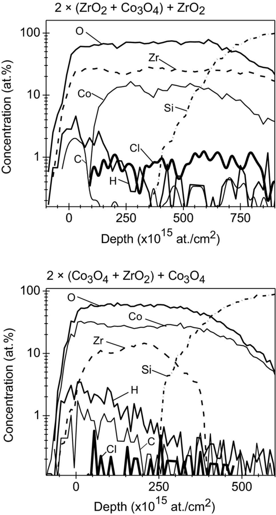
Figure 1. Elemental depth profiles determined by ToF-ERDA for the 2 × (ZrO2 + Co3O4) + ZrO2 (upper panel) and 2 × (Co3O4 + ZrO2) + Co3O4 (lower panel) nanolaminates in the as-deposited state. The title above the graph indicates the type of nanolaminate.
Scanning electron microscope images demonstrated that the surfaces in the case of all four thin film structures (Fig. 2) were quite uniformly covered by grain-like features, which may easily be connected to crystallization, and also indicate that the deposition temperature of 300°C was high enough to cause crystallization in both Co3O4 and ZrO2 thin films. The similarity between those thin film multilayer structures that had the same type of oxide as the topmost layer implies that in the case of nanolaminates, the layers are probably not mixed and the upmost layer is indeed the oxide layer that was defined in the ALD experiment and displayed on the explanatory schematics (Fig. 2). One can also notice that the charging effect has taken place in the case of the ZrO2 layers, which can be seen by the bright white areas. This effect is more characteristic of the non-conductive (insulating) materials. In Ramesh et al.62 it has been stated that, in order to be ferroelectric, a material must be insulating (otherwise the mobile charges would screen out the electric polarization).
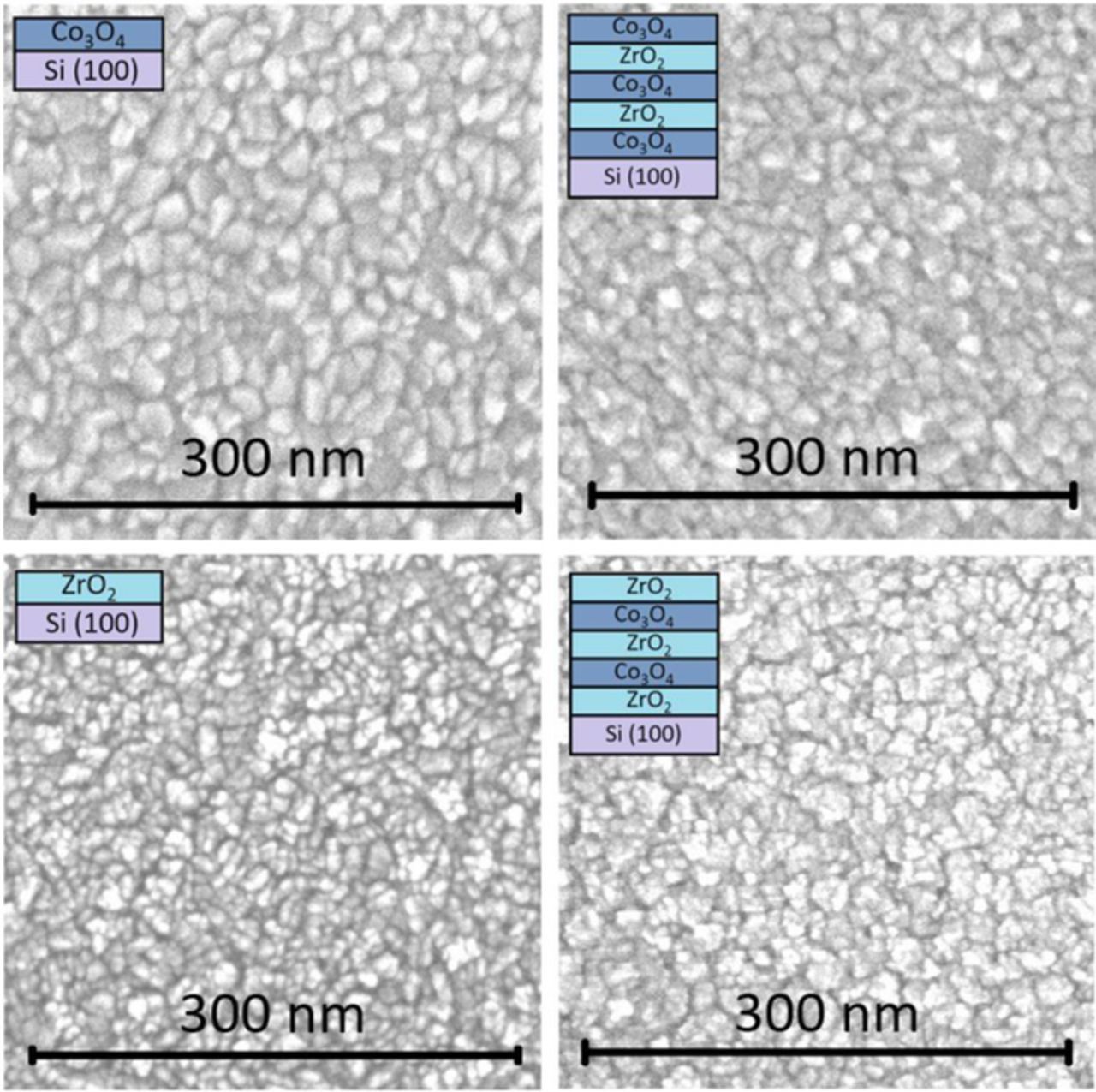
Figure 2. The bird-eye view of the scanning electron microscope images of ZrO2 and Co3O4 thin films and ZrO2-Co3O4 nanolaminates as-deposited with explanatory schematics indicating the order and the amount of layers deposited.
GIXRD (Fig. 3) confirmed that the reference thin films and ZrO2-Co3O4 nanolaminates were all crystallized already in the as-deposited state. The diffractogram of the reference ZrO2 thin film (Fig. 3) contained five reflections 111, 200, 220, 311 and 222 at 30.5°, 35.2°, 50.6°, 60.3° and 63.2°, respectively, attributable to cubic ZrO2 phase (PDF card 00-027-0997). Reflections  11, 111 and 131 at 28.2°, 31.5°, 59.8°, respectively, could be attributed to the monoclinic ZrO2 phase (PDF card 00-037-1484). In an earlier study,46 the formation of both cubic and monoclinic ZrO2 phases in the thin films deposited at the same temperature and from the same precursors has been described.
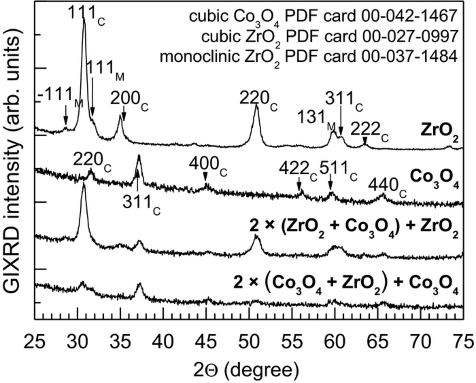
Figure 3. X-ray diffraction patterns from the Co3O4 and ZrO2 thin films and ZrO2-Co3O4 nanolaminates, in the as-deposited state. Miller indexes assigned after crystallization are indicated with "C" for cubic and "M" for monoclinic phase.
In the diffractogram of the reference Co3O4 thin film, six peaks attributable to the 220, 311, 400, 422, 511 ja 440 reflexes from the cubic phase were detected at 31.3°, 36.9°, 44.8°, 55.7°, 59.4° and 65.2° (PDF card 00-042-1467). In an earlier study by Klepper et al.63 on Co3O4, atomic layer deposited at 283°C, the cubic phase has also been detected. While comparing the diffractograms of the nanolaminates one could notice that in the case of the nanolaminate, that had the ZrO2 as the top-most layer, the peak intensities were noticeably higher and therefore the interlayers must be more ordered compared to the nanolaminate that had Co3O4 as the top-most layer. Probably the dominant phase is the cubic ZrO2 polymorph, although the tetragonal and/or orthorhombic ZrO2 in the phase composition cannot be completely ruled out.
In STEM images made of both types of nanolaminates (Fig. 4, the leftmost-panel of (a) and (b)), five distinct metal oxide layers grown sequentially on the Si substrate can be seen. Cross-sectional EDX composition profiling of the ZrO2-Co3O4 nanolaminates in the as-deposited state (Fig. 4, 4 small panels of (a) and (b) on the right) showed that in the case of the 2 × (Co3O4 + ZrO2) + Co3O4 nanolaminate, three chemically distinct cobalt-containing and two zirconium-containing layers alternated as expected. In the case of 2 × (ZrO2 + Co3O4) + ZrO2 one can see three alternating zirconium and two cobalt-containing layers. Therefore, the structure of the nanolaminates corresponded to the schematics described in the experimental section. In the case of both nanolaminates, the oxygen signal was detected relatively homogeneously across all five metal oxide layers, as expected. One can also see that the thicknesses of the oxide layers are quite similar indeed, except that in the case of the first layer of 2 × (Co3O4 + ZrO2) + Co3O4 nanolaminate, where the cobalt oxide occurred slightly thicker compared to the other layers.
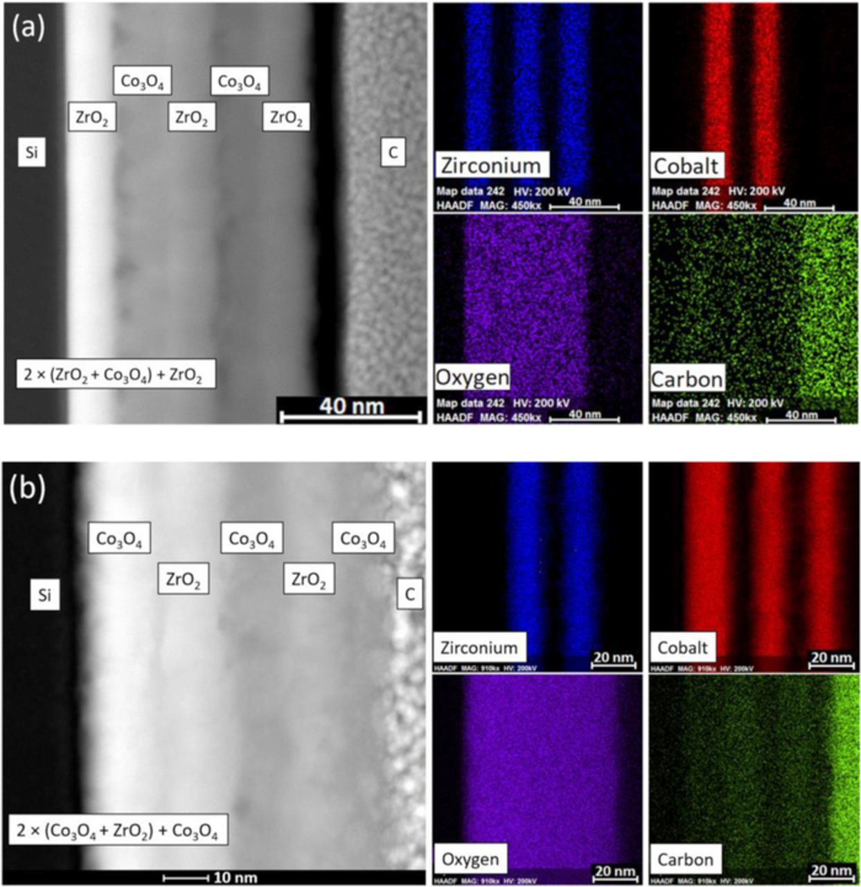
Figure 4. Cross-sectional EDX composition profiling of the (a) 2 × (ZrO2 + Co3O4) + ZrO2 nanolaminate and (b) 2 × (Co3O4 + ZrO2) + Co3O4 nanolaminate in the as-deposited state. STEM images of the site of interest are displayed on the left panels. The elements detected are indicated by labels and colors displayed on the right panels. Carbon on top of the layers originates from lamellae creation process where it acted as a protective layer.
Comparison of STEM images and EDX composition profiling made of both types of nanolaminates (Fig. 5) revealed that slight mixing of oxide layers at the interfaces between two oxides has occurred in both cases. Nevertheless, the appearance of distinguishable lattice planes is indicative of ordered structure. In the case of the 2 × (ZrO2 + Co3O4) + ZrO2 nanolaminate the STEM image taken from one other location (Fig. 6) revealed probably a local phenomenon in the form of apparently round features. An apparently similar phenomenon has earlier been observed in the case of atomic layer deposited Ho2O3-TiO2 nanolaminates64 where Ho2O3 and TiO2 layers were mixed after annealing and the nanolaminate structure was destroyed. If these features were hollow, then the appearance of such regions could be associated with the Kirkendall effect that can arise when two distinct materials are placed in contact to each other and their interdiffusion occurs by a vacancy mechanism. In the context of the present work, however, Kirkendall effect should be considered with caution and this phenomenon therefore would need further investigation. In our study, these round features are likely not voids due to the appearance of distinguishable lattice planes within those round features.
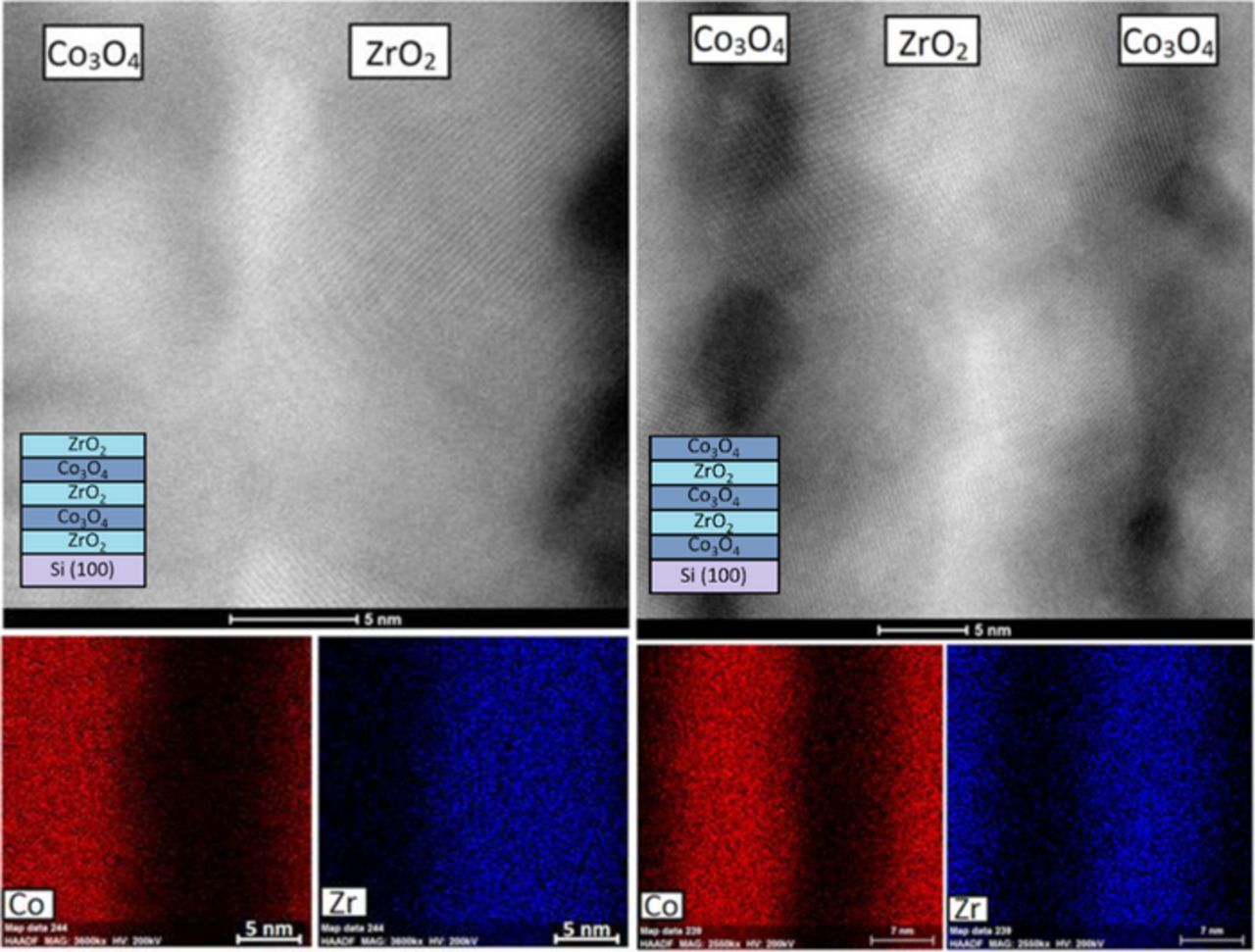
Figure 5. Cross-sectional STEM image and EDX composition profiling taken from the lamellae that were made of the nanolaminates in the as-deposited state. 2 × (ZrO2 + Co3O4) + ZrO2 nanolaminate on the left panels and 2 × (Co3O4 + ZrO2) + Co3O4 on the right panels.
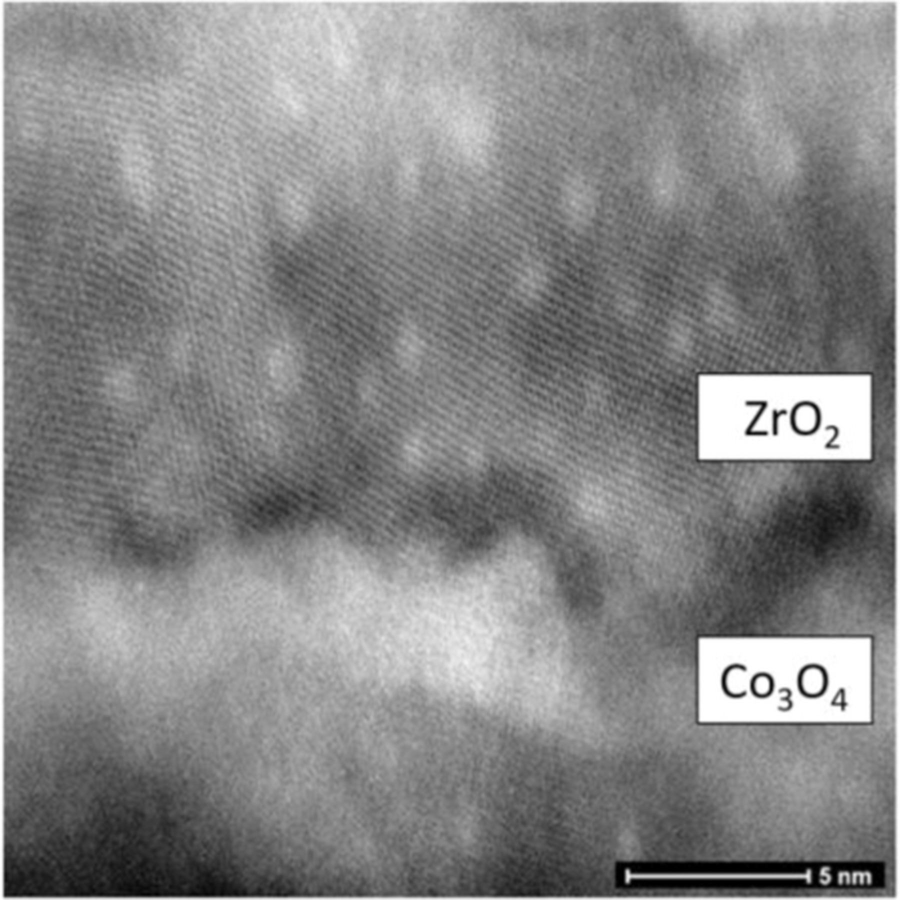
Figure 6. Cross-sectional STEM image taken of the 2 × (ZrO2 + Co3O4) + ZrO2 nanolaminate.
Magnetic and electrical behavior
In-plane magnetic measurements were performed for as-deposited ZrO2-Co3O4 nanolaminates and reference ZrO2 and Co3O4 thin films. The structures demonstrated ferromagnetic-like behavior at room temperature with saturation magnetization (Fig. 7) and could therefore be described as rather soft ferromagnetics. In the M–H curves the saturation magnetization values for the ZrO2 and Co3O4 were 3.7 × 10⁻⁶ emu and 3.5 × 10⁻⁶ emu at 300 K, respectively. One can also notice that the 2 × (ZrO2 + Co3O4) + ZrO2 nanolaminate showed several times higher saturation magnetization (1.7 × 10⁻⁵ emu) compared to the other samples. The coercivity values of films were low, ranging from around 24 to 60 Oe (1.9 to 4.8 kA/m), evaluated from their very narrow hysteresis loops.
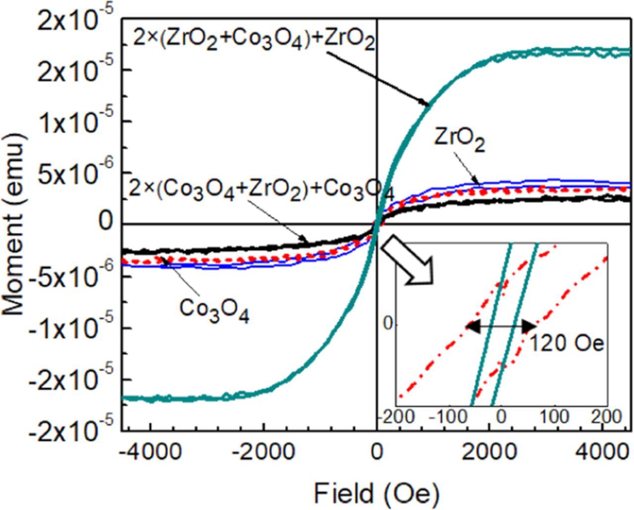
Figure 7. Magnetic moment vs. external magnetic field (M–H) curves for the as-deposited ZrO2-Co3O4 nanolaminates and ZrO2 and Co3O4 reference thin films measured at room temperature (300 K).
At first, it might be a bit surprising to see that the nanolaminate that had three layers of ZrO2 and two layers of Co3O4 possessed that much better magnetic polarization compared to the laminate that had one more Co3O4 layer and one less ZrO2 layer. On the other hand, the magnetic behavior of ZrO2 thin films and nanoparticles has been reported before,65–68 and the magnetism was largely attributed to the formation and presence of oxygen deficient metastable zirconia phases. In the present study, it was confirmed, that the solid structures deposited do not consist of stable crystallographic phases characteristic of perfectly stoichiometric zirconium dioxide. It is likely that the deposited oxides have not been fully oxidized due to the low deposition temperature. Thus, noticeable magnetization is likely caused by a significant contribution from nanocrystalline cubic tetragonal ZrO2 phase.
From the resistive switching loops (Fig. 8) one can see that both samples show bipolar behavior, but with opposite sign. In the sample Si/TiN/2 × (Co3O4 + ZrO2) + Co3O4/Pt (Fig. 8, lower panel) the transition from low to high resistance states (SET)69,70 occurs for negative voltages between −1.5 and −2.5 V, whereas the transition from high to low resistance state (RESET) occurs for positive voltages in the range of 2.0–3.5 V. It can also be noticed that both transitions are very sharp and currents at the low resistance state are more than one order of magnitude higher than at the OFF state. On the contrary, in the sample Si/TiN/2 × (ZrO2 + Co3O4) + ZrO2/Pt (Fig. 8, upper panel) SET occurs at positive of about 6 V, whereas RESET occurs at negative voltages in the range of −6–(−8) V, and both transitions are very gradual. Moreover, it is evident that the loops are much narrower.
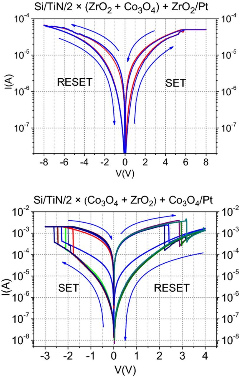
Figure 8. Current-voltage curves measured from the Si/TiN/2 × (ZrO2 + Co3O4) + ZrO2/Pt (upper panel) and Si/TiN/2 × (Co3O4 + ZrO2) + Co3O4/Pt (lower panel) MIM samples.
The opposite sign of the bipolar loops can be related to the different ordering of the multilayers. The conductive filaments in this kind of materials are typically formed due to the accumulation of oxygen vacancies, which cluster, so connecting top and bottom electrodes (set process). Oxygen vacancies are caused due to the migration of negative oxygen ions due to the electric field. RESET process is based on the opposite mechanism: oxygen anions are moved from the metal to the insulator and backfill the vacancies to annihilate the conductive path. Therefore, the negative reset voltage indicates that oxygen atoms coming from the top electrode cause the conductive filament oxidation in the adjacent insulator, that is, in the upper dielectric region. That is the case of sample Si/TiN/2 × (ZrO2 + Co3O4) + ZrO2/Pt, where the upper film is ZrO2, which is in contact with the top Pt electrode. Pt is reputed to be highly active as an oxygen repository in bipolar switching devices (in contrast, TiN used to be very inactive). In a Si/TiN/2 × (Co3O4 + ZrO2) + Co3O4/Pt nanolaminate, where the Co3O4 layer is in contact with both of the electrodes, SET and RESET occurs for negative and positive voltages, respectively. Moreover, current loops are wider than for the Si/TiN/2 × (ZrO2 + Co3O4) + ZrO2/Pt sample. Tentative explanation is that in these samples, the dominant mechanism is the migration of Co cations to the ZrO2 insulation layer, that is, resistive switching is caused by the electrochemical metallization of the ZrO2 layer.
The charge polarization – voltage (P-V) hysteresis loops measured during the Sawyer-Tower measurements for the Si/TiN/2 × (Co3O4 + ZrO2) + Co3O4/Pt (Fig. 9) and Si/TiN/2 × (ZrO2 + Co3O4) + ZrO2/Pt (not shown) samples were not promising. The charge polarization was about 55 nC at 0 V for the Si/TiN/2 × (Co3O4 + ZrO2) + Co3O4/Pt nanolaminate and 0.6 nC at 0 V for the Si/TiN/2 × (ZrO2 + Co3O4) + ZrO2/Pt nanolaminate. The shape of those loops is typical to a lossy dielectric and therefore not characteristic to a ferroelectric material.71
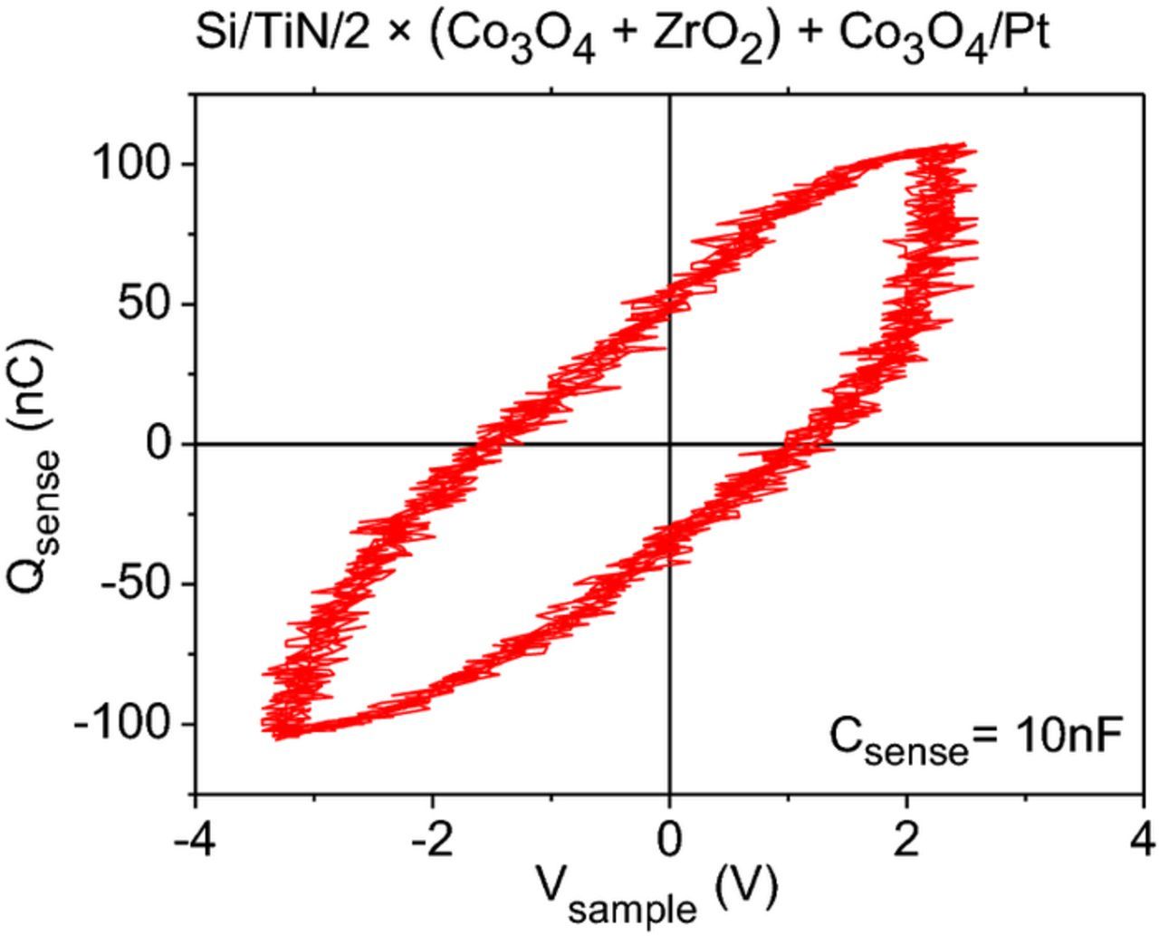
Figure 9. P-V curves of the Si/TiN/2 (Co3O4 + ZrO2) + Co3O4/Pt recorded during the Sawyer-Tower measurements. The value of Csense was 10 nF.
In general, the films grown in the present study performed as moderately insulating dielectric metal oxides. The capacitance measurements revealed that the oxide layers in metal-oxide-nitride exhibited dielectric dispersion behavior rather common in high-permittivity oxide materials. The permittivity values measured in these laminates evidently exceeded 30–35 at measurement frequencies ranging from 1 to 10 kHz (Fig. 10), which can be explained by considerable contribution of metastable crystalline ZrO2 phases in the films. However, in the laminate with structure of 2 × (Co3O4 + ZrO2) + Co3O4 the apparent permittivity value at relatively low frequencies approached values as high as 100, which is most likely due to high leakage in the films and concurrent interface or space charge polarization.
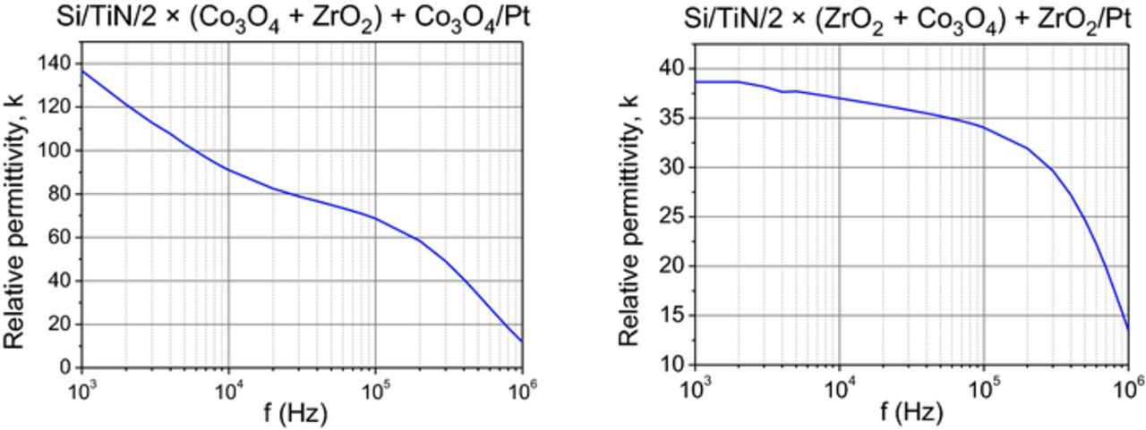
Figure 10. Permittivity dispersion in the nanolaminate films with structures denoted by labels.
In the five-layer nanolaminates investigated in the present study, the dominance of metastable ZrO2 polymorphs (cubic/tetragonal) over the monoclinic phase appeared somewhat clearer compared to that observed earlier in ZrO2/Co3O4 double layers,59 decided on the basis of XRD results. Concurrently, the saturation magnetization tended to be higher, although differences in the magnetization hysteresis width occurred insignificant. Charge polarization in the capacitor structures did not differ essentially in nanolaminates and double layers. At the same time, nanolaminates in the present study tended to demonstrate somewhat wider window between high and low resistance states, as measured in the resistive switching regime. The high resistance state was thereby realized at lower current values, which may expected to be advantageous when aiming at lowered power consumption during the information reading process, if such materials were applied in memristor cells.
Summary
ZrO2-Co3O4 nanolaminates were grown by atomic layer deposition. The films consisting of distinct metal oxide layers were formed. The performance of the laminate films was dependent on the relative content of constituent oxide layers. The structure that consisted alternately of three ZrO2 and two Co3O4 layers showed higher magnetization compared to the structure that consisted alternately of three Co3O4 and two ZrO2 layers. All studied structures exhibited characteristics that are inherent to ferro- or ferrimagnetic materials like saturation magnetization and non-linear relationship between magnetic moment and external magnetic field. Electrical measurements revealed formation of significant polarization versus external field loops, probably markedly influenced by interfacial polarization and both samples showed bipolar behavior in resistive switching regime, although with an opposite sign.
Acknowledgments
The authors of the paper are thankful to Alma-Asta Kiisler for the technical assistance in sample preparation, to Jekaterina Kozlova for sharing her support and knowledge in connection with the lamellae creation process, to Peeter Ritslaid for his support in XRF studies and to Dr. Aarne Kasikov for depositing the electrodes and ellipsometric measurements. The study was partially supported by the European Regional Development Fund project "Emerging orders in quantum and nanomaterials" (TK134), Estonian Academy of Sciences (SLTFYPROF), Estonian Research Agency (IUT2-24, PRG4) and Spanish Ministry of Economy and Competitiveness (TEC2017-84321-C4-2-R) with support of Feder funds.
ORCID
Helina Seemen 0000-0002-4850-0851
Kristjan Kalam 0000-0001-5934-1860
Timo Sajavaara 0000-0003-2235-7441
Salvador Dueñas 0000-0002-2328-1752
Helena Castán 0000-0002-3874-721X
Raivo Stern 0000-0002-6724-9834
Kaupo Kukli 0000-0002-5821-0364
Aile Tamm 0000-0002-0547-0824