Abstract
Selectively activated p-type regions are necessary for many electronic devices that require planar processing. The standard process of implanting p-type dopants, such as Mg, in GaN is notoriously more difficult than in other material systems, as the extremely high temperatures required to activate the implanted Mg also damage the GaN surface. In this research, a novel annealing technique is introduced for this purpose – symmetric multicycle rapid thermal annealing (SMRTA). It is shown that SMRTA is superior to the earlier developed multicycle rapid thermal annealing (MRTA) in terms of improvement of the crystalline quality of implanted GaN. The SMRTA technique was applied to Mg-implanted GaN to realize a rectifying junction. The annealing process detailed in this research will be a key enabling step for future GaN-based devices that require planar processing with selective area implants.
Export citation and abstract BibTeX RIS

This is an open access article distributed under the terms of the Creative Commons Attribution 4.0 License (CC BY, http://creativecommons.org/licenses/by/4.0/), which permits unrestricted reuse of the work in any medium, provided the original work is properly cited.
GaN and other III-nitride based semiconductors have received a great deal of attention from the research community due to favorable material properties which include a tunable direct bandgap, radiation hardness, and a favorable Baliga figure of merit compared to Si and SiC.1,2 The doping of p-type GaN during growth is challenging and has been the focus of numerous studies because it has many potential transformative applications in power electronics and optoelectronics.3
P-type dopant implantation and activation adds additional complexity to the synthesis of p-type GaN. The ability to implant and activate p-type species in GaN is a key enabling process for devices that require selective area doping. Device structures that benefit from the ability to selectively implant and activate p-type dopants in GaN include implanted guard rings for electric field spreading, implanted current blocking layers for current aperture vertical electron transistors, and implanted regions below contacts to lower contact resistance.4,5 Unfortunately, the implantation and activation of Mg in GaN is difficult because of the high temperatures required (over 1300°C) for the activation anneal,6 which are significantly higher than the decomposition temperature of GaN at atmospheric pressures (845°C).7 The decomposition of GaN occurs due to a loss of nitrogen and results in surface damage and the formation of N vacancies, which are compensating donors.8
To avoid GaN decomposition at the elevated annealing temperatures required for Mg activation, high pressure environments and non-equilibrium annealing conditions combined with capping layers have been investigated.9,10 GaN can be successfully annealed at about 1500°C, but a 1.5 GPa overpressure of N2 is necessary to avoid surface degradation.11 Such high gas pressures also require a complicated experimental setup and are not easily industrial scalable.12
A second, more scalable, alternative to the high pressure annealing of GaN relies on using non-equilibrium annealing conditions. For this type of annealing, a capping layer is used to prevent nitrogen loss from the GaN surface. Depending on the material, structure, and thickness of the capping layer, higher annealing temperatures can be applied without GaN decomposition compared to uncapped GaN. Capping materials that have been previously studied include MgO, graphite, AlN, and Si3N4.13,14 Previous efforts to electrically activate implanted Mg in GaN using different annealing techniques such as rapid microwave thermal annealing have been met with limited success.15 More recently, the development of a multicycle rapid thermal annealing (MRTA) technique has enabled Mg activation after implantation with activation efficiencies of over 8%.6,16 MRTA utilizes the repetition of heating pulses to anneal GaN at temperatures above 1300°C. By successively pulsing the temperature over multiple cycles, the aggregate time above 1300°C can reach long durations (minutes) while preserving the integrity of the GaN. Additionally, an AlN cap is used in the MRTA process to prevent nitrogen loss at the GaN surface.6
The MRTA process consists of two separate, consequent steps (Fig. 1a). Both steps are conducted at an elevated nitrogen pressure of about 24 bar.6 First, the implanted GaN is annealed conventionally at a temperature where the capped GaN is stable on the order of 10's of minutes. The nitrogen overpressure increases the temperature stability range of GaN to around 1000°C.6 This first step partially restores the implant-induced crystal damage,17 which leads to a more thermodynamically stable crystal structure. The improved stability afforded by the conventional annealing step prepares the GaN lattice for the second step. The second step of the MRTA process includes rapid heating pulses to temperatures above the conventional annealing temperatures (1000°C) to accumulate longer total times of GaN exposure to increased temperatures. The rapid heating/cooling cycles are kept very short, on the order of tens of seconds, to avoid nitrogen buildup under the capping structure.
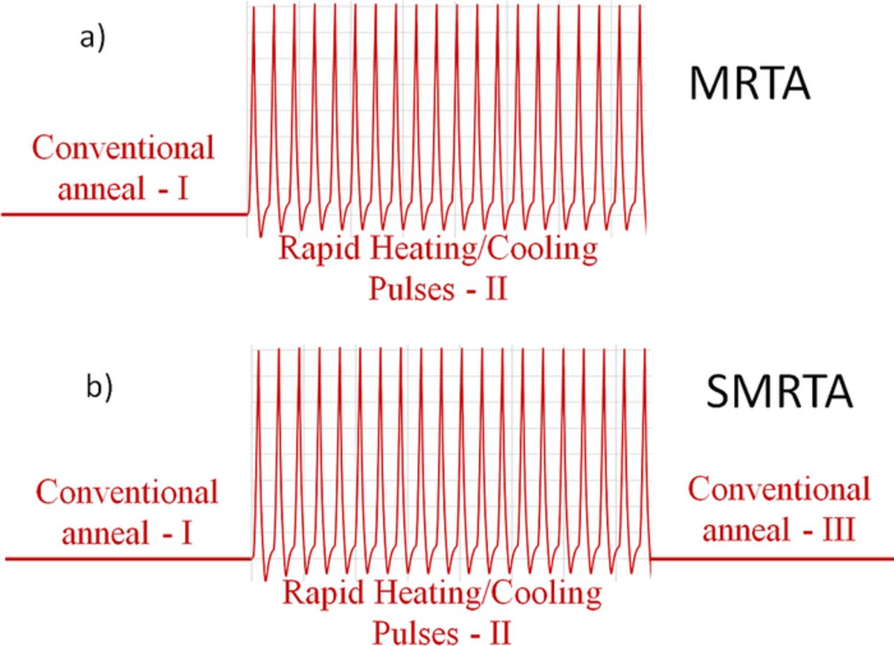
Figure 1. Schematic of the temperature profiles for the MRTA (a) and SMRTA (b) annealing processes. The MRTA annealing process includes a preliminary conventional anneal followed by rapid heating pulses. The SMRTA annealing process includes a preliminary conventional anneal, rapid heating pulses, and a secondary conventional anneal after the heating pulses.
In this paper, we introduce a modified MRTA process that has enabled the realization of a rectifying junction through Mg-implantation of GaN. The modified MRTA process includes an additional conventional annealing step after the multiple rapid heating and cooling cycles as shown in Fig. 1b. This work demonstrates the necessity of this additional step to remove detrimental structural changes in GaN introduced by the rapid heating and cooling cycles. The new, modified process consists of two conventional annealing steps, one before and one after the rapid heating pulses (Fig. 1b), thus it is designated symmetrical multicycle rapid thermal annealing (SMRTA).
Experimental
The investigation of the improved SMRTA process was carried out with four experiments. The first two experiments (A and B) consisted of a comparison between MRTA and SMRTA in terms of crystal lattice restoration. The second two experiments (C and D) were carried out to study and demonstrate the improved electrical properties of Mg-implanted GaN annealed with the SMRTA process. The processing of all samples included a conventional anneal at 1000°C for 30 minutes, followed by rapid thermal pulsing. For MRTA processes, we denote this as MRTA/T/x, where T is the max temperature of the pulse and x is the number of cycles. For SMRTA, a similar naming convention is used, but the process is followed by an anneal with the same (symmetrical) conditions as the pre-pulsing anneal.
The two samples used in the first experiment (A) were grown on a sapphire substrate by metal organic chemical vapor deposition (MOCVD) and consisted of 2 μm of GaN with a dual-layer grown AlN capping structure. The first thin AlN layer (4 nm) was grown at high temperature (1100°C) for an improved interface without cracking.6 The second AlN layer (25 nm) was grown at 660°C and was included for mechanical support.6 An additional 250 nm thick AlN layer was sputtered on the surface of the MOCVD grown AlN stack to provide additional protection for the underlying GaN. This additional sputtered cap provided further mechanical support and has been previously shown to improve the resilience of the MOCVD AlN cap.18 The samples were masked using photoresist so that half of each sample remained unimplanted, and were implanted at room temperature with the doses and energies shown in Fig. 2. These energies and doses were chosen for a constant Mg concentration of approximately 1 × 1019 cm−3 as shown by the SRIM simulation in Fig. 2. The samples were split, with one annealed with the MRTA/1350/40 process and the other undergoing SMRTA/1350/40 process. The same implanted Mg ion dose of 4.6 × 10¹⁴ atoms/cm2 was used for both samples. The MRTA process was comprised of a conventional anneal at 1000°C for 30 minutes, followed by 40 rapid heating and cooling cycles with a peak temperature of 1350°C. The SMRTA process had the same conventional anneal and pulse process, but the process was followed by an additional conventional anneal at 1000°C for 30 minutes.
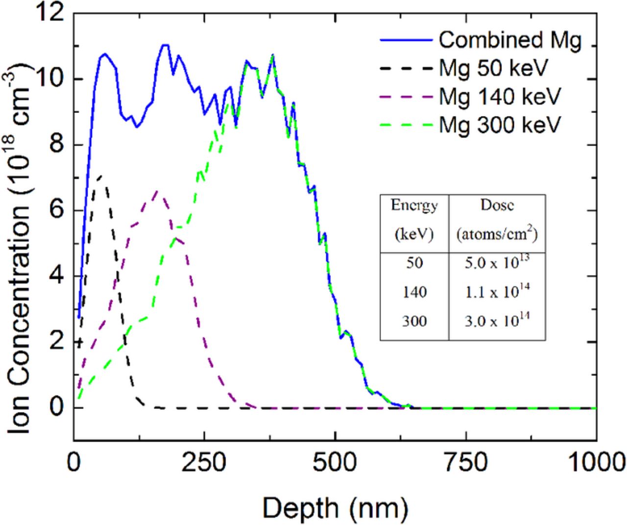
Figure 2. SRIM simulated implantation profile and conditions for the samples studied. The implantation energies and doses were chosen for a constant Mg concentration of approximately 1 × 1019 cm−3.
The second experiment (B) systematically studied the effects of sequential stages of the SMRTA process on the GaN crystal quality. In this experiment, each stage of the SMRTA process was examined on one sample. The sample used in the second experiment consisted of the same structure and implant profile as in (A), but the sample was unmasked for a blanket implantation performed at 500°C. The first stage of this experiment was the MRTA process, which consisted of a conventional anneal at 1000°C for 30 minutes followed by a single pulse at a maximum temperature of 1270°C (MRTA/1270/1). After this MRTA/1270/1 treatment, the sample was characterized using Raman spectroscopy. The sample was then annealed again with only a conventional anneal at 1000°C for 30 minutes, which essentially represents the third stage of the SMRTA/1270/1 process, and characterized once more after the anneal. To demonstrate the efficacy of the SMRTA process in reversing damage caused by thermal stresses at different temperatures, the sample was then subsequently annealed using a single pulse to 1460°C (MRTA/1460/1) and characterized again. Finally, the sample was conventionally annealed for 30 minutes at 1000°C, resulting in the SMRTA/1460/1 process, and characterized.
The third experiment (C) was performed to demonstrate the benefits of SMRTA over MRTA in terms of electrical activation of the implanted Mg. The two samples in (C) had the same structure and implantation schedule as samples in (A). One sample was annealed using MRTA/1350/20 while the second was annealed with SMRTA/1350/20. After annealing, the AlN protective capping layers were removed using AZ400 K, a photoresist developer that selectively etches AlN without damaging the underlying GaN, heated at 80°C.19,20 The conductivities of the two samples were compared after depositing metal contacts on the surface, which were patterned by lift-off of electron-beam evaporated Pd/Au. The metal stack consisted of 20 nm Pd and 100 nm Au. Pd is a high work function metal that has been shown to form ohmic contacts to p-type GaN.21
Finally, experiment (D) extended the SMRTA process in demonstrating a vertical p-i-n junction, with the p-type layer formed by implanted, annealed Mg. The sample structure included 8 μm of MOCVD-grown unintentionally-doped GaN (Agnitron Technology) on a bulk, HVPE n-type substrate (Kyma Technologies). The sample was implanted at room temperature using a box implant profile for an Mg concentration of 2 × 1019 cm−3 for a depth of 500 nm. The total ion implantation dose used in experiment D was 7.1 × 10¹⁴ atoms/cm2. The sample was capped on both sides with 250 nm of sputtered AlN. AZ400 K was used to remove the AlN capping layer and Pd/Au contacts were used to contact the Mg-implanted layer. A 100 nm Al contact was used to contact the n-type bulk GaN substrate.
Characterization performed on the samples includes AFM using a Bruker FastScan system for assessing the surface morphology. Raman spectroscopy was utilized for characterizing the crystal quality before and after annealing using a Thermo Scientific DXRxi Raman system equipped with a 532 nm laser. Electrical characterization was performed using a Keithley 4200 semiconductor characterization system.
Results and Discussion
Raman spectroscopy is a powerful technique for probing the crystal structure of implanted and annealed GaN films. As shown in Fig. 3, the as-implanted Raman spectrum includes several peaks other than those for the GaN or the substrate modes. These extra modes have been attributed to vacancy and vacancy cluster related modes.22,23 However, after annealing, these peaks are no longer detected and thus the annealing is able to remove most of the implantation damage. It should also be noted that the sapphire substrate is barely detectable in the Raman spectra, indicating that the method is surface sensitive and thus is suitable for characterizing the implanted portion of the GaN. To quantitatively determine the effects of the different annealing processes compared herein, the full width at half-maximum (FWHM) of the E2 Raman modes of experiment (A) were compared and plotted in Figure 4. The FWHM of the E2 Raman mode decreases as the crystal quality of GaN improves.24 Since half of each sample in experiment (A) was masked during implantation, a comparison between the implanted and as-grown portions can be conducted. The as-implanted FWHM of the E2 mode is broad due to implantation-induced defects, while the as-grown portion has a much narrower FWHM. After the MRTA/1350/40 process, the FWHM of the implanted GaN E2 Raman mode decreases, indicating that the crystal quality has partially recovered from the implantation damage. At the same time, the FWHM of the E2 Raman mode of the as-grown part of the sample has increased after the standard MRTA process, implying that the standard MRTA process resulted in a slight degradation of the GaN crystalline quality. These detrimental structural changes can be attributed to the formation of defects formed and quenched during rapid heating and cooling cycles. When undergoing SMRTA/1350/40, with the additional anneal post-thermal pulsing, the crystal quality of both the implanted and as grown regions of the sample substantially improved in comparison with the crystal quality of these regions after the standard MRTA process. From the data in Fig. 4, it can be concluded that SMRTA returns the FWHM of the as-grown portion to nearly the as-received crystal quality.
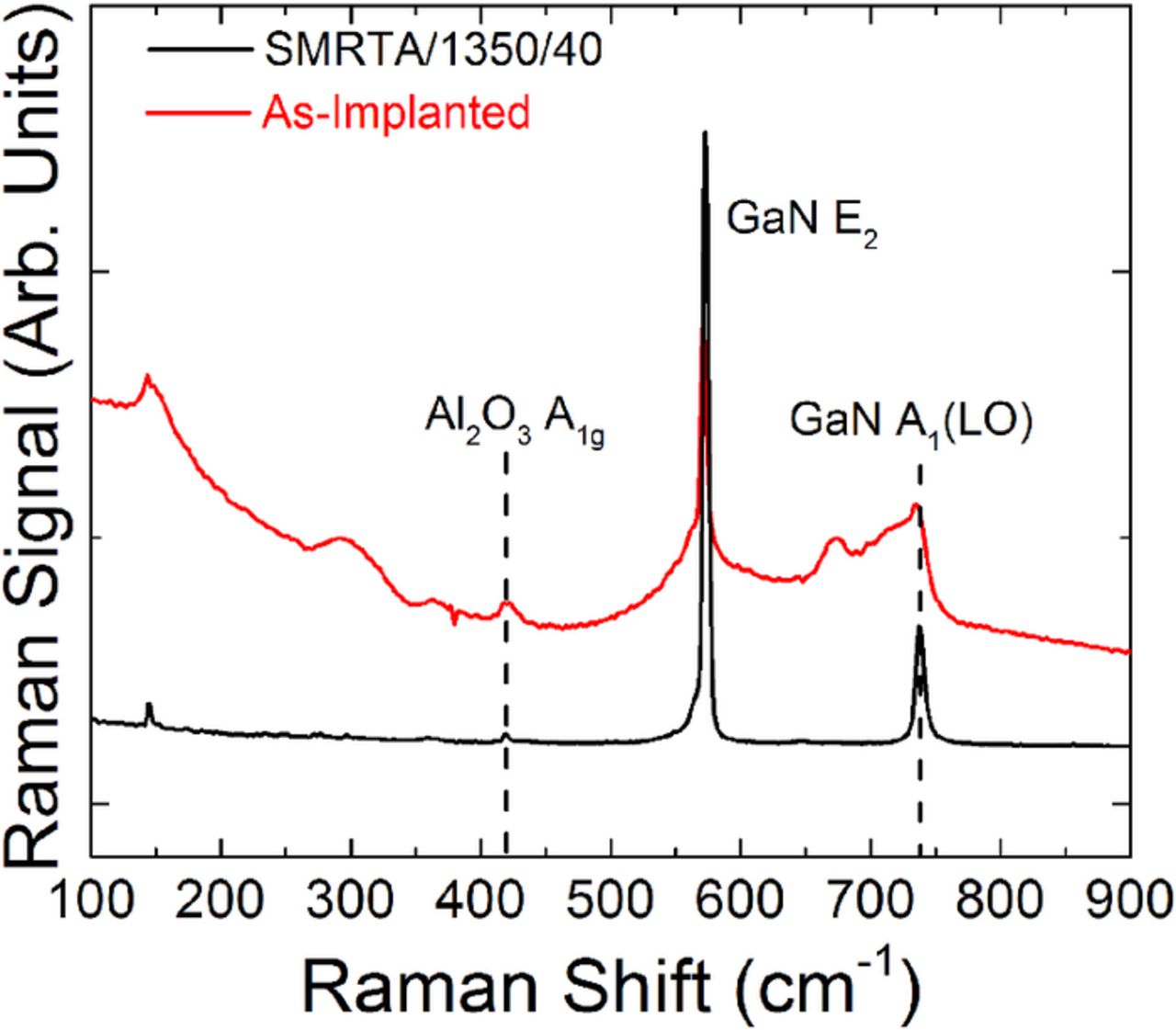
Figure 3. Raman spectra of an implanted and SMRTA-annealed sample. Before annealing, several additional peaks are evident other than the GaN and Al2O3 substrate peaks. These extra peaks are attributed to vacancy and vacancy cluster related modes, and they are no longer detected after annealing using the SMRTA process.
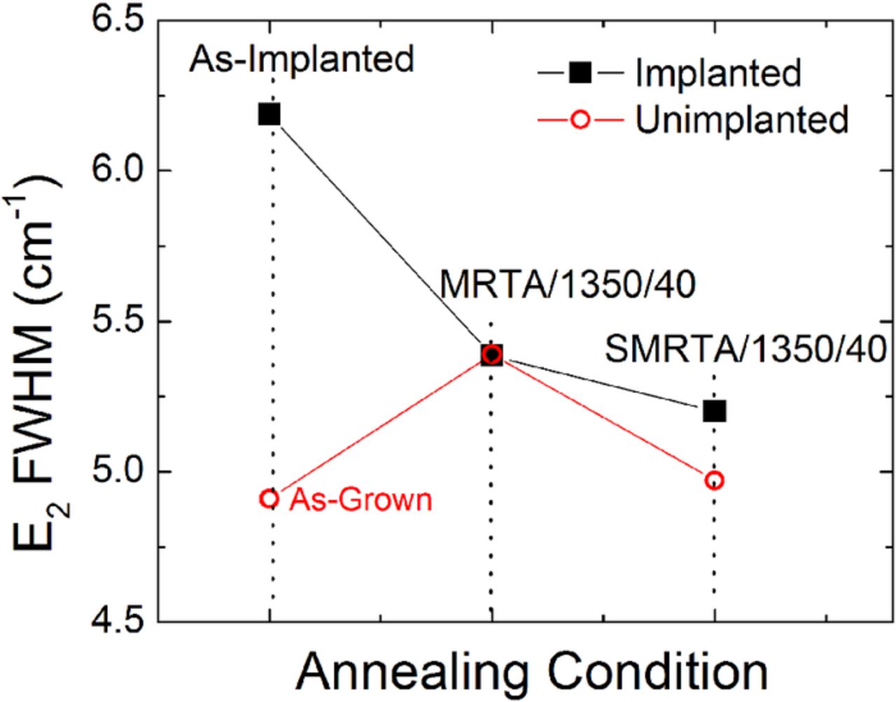
Figure 4. Comparison of the E2 FWHM before and after different annealing conditions in both the implanted and unimplanted regions of the samples. After the MRTA treatment, the as-implanted FWHM decreases dramatically while the unimplanted (as-grown) FWHM increases, indicating that the MRTA process induces defects through the rapid heating and cooling stresses. However, after the SMRTA process, both the implanted and unimplanted FWHM's decrease, confirming that the SMRTA process is effective in removing some of the crystal structure degradation caused by the MRTA process.
The rapid heating and cooling cycles, while successful in providing sufficiently high temperatures for sufficient time to remove implantation damage and activate Mg, also may introduce defects into the GaN film. However, as it is shown in Fig. 4, these detrimental structural changes can be reversed by using SMRTA. Hence, the additional conventional anneal after the rapid heating and cooling cycles improves the outcome of the annealing process by reversing some of the structural changes in the lattice introduced by the thermal pulses.
To further assess the effects of the MRTA and the SMRTA techniques and study the effects of sequential steps of the SMRTA process on the GaN crystal quality, pulses at different temperatures were implemented in experiment (B) on a single implanted sample with the same implantation profile shown in Fig. 2. As implanted, the FWHM of the E2 mode is quite broad at 5.64 cm−1 due to implantation-induced defects. However, this is a narrower FWHM than observed in the previous set of samples in experiment (A), due to the higher implantation temperature (500°C vs room temperature). After a MRTA/1270/1 process, the FWHM decreased to 5.35 cm−1, indicating an improvement in the crystal quality (Fig. 5). After an additional conventional anneal at 1000°C for 30 minutes, the crystal quality further improved, as shown in Fig. 5. This additional conventional anneal combined with the previous MRTA regime represents SMRTA/1270/1. We then treated the sample with a single high temperature pulse to 1460°C, which increased the E2 FWHM and thus reduced the crystal quality of the GaN due to the structural changes introduced with the rapid heating pulse (labeled MRTA/1460/1 in Fig. 5). After an additional 1000°C anneal for 30 minutes (labeled SMRTA/1460/1 in Fig. 5), the FWHM once again decreased even more than after the SMARTA/1270/1, because the pulse to 1460°C is more efficient in removing implantation damage than the pulse to 1270°C. Thus, the rapid high temperature pulse is effective for removing defects and defect complexes introduced by Mg implantation, but this pulse also creates other defects in the film. The post-pulse 1000°C conventional annealing steps relieve these defects.
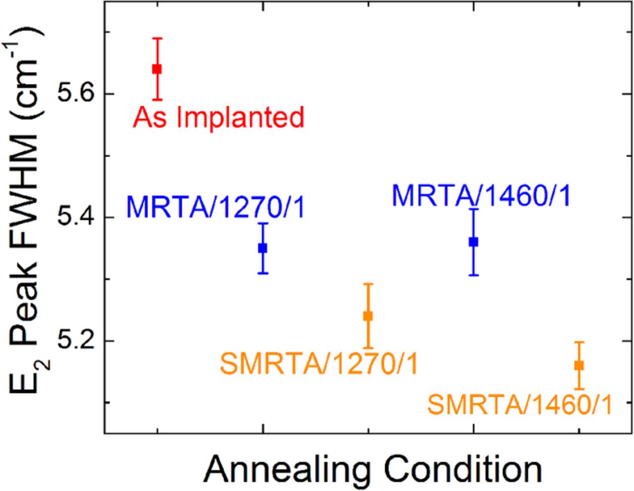
Figure 5. Raman E2 mode FWHM comparison for different annealing stages on the same sample. After the MRTA/1270/1 process, the FWHM decreases compared to the as-implanted FWHM. The FWHM further decreases after the SMRTA/1270/1 process. However, after annealing the sample with the an additional pulse at 1460°C (MRTA/1460/1), the FWHM increases, implying that the crystalline quality degrades due to the rapid heating and cooling cycles. After another conventional anneal (marked SMRTA/1460/1), the FWHM decreases even further than the previous SMRTA/1270/1 FWHM.
After the final pulse and anneal iteration of experiment (B), AFM was performed to compare the surface morphology of the AlN-capped GaN before and after implantation and annealing. As shown in Fig. 6, the surface morphology is unchanged between the as-grown and the consecutive SMRTA processes terminating at 1460°C. No cracks or other signs of damage were observed on the surface of the sample after annealing as shown in Fig. 6. The RMS roughnesses before and after annealing are essentially unchanged at 1.55 and 1.65 nm, respectively. Thus, the capping structure used in this research is able to effectively withstand the high temperatures of both the MRTA and SMRTA processes.
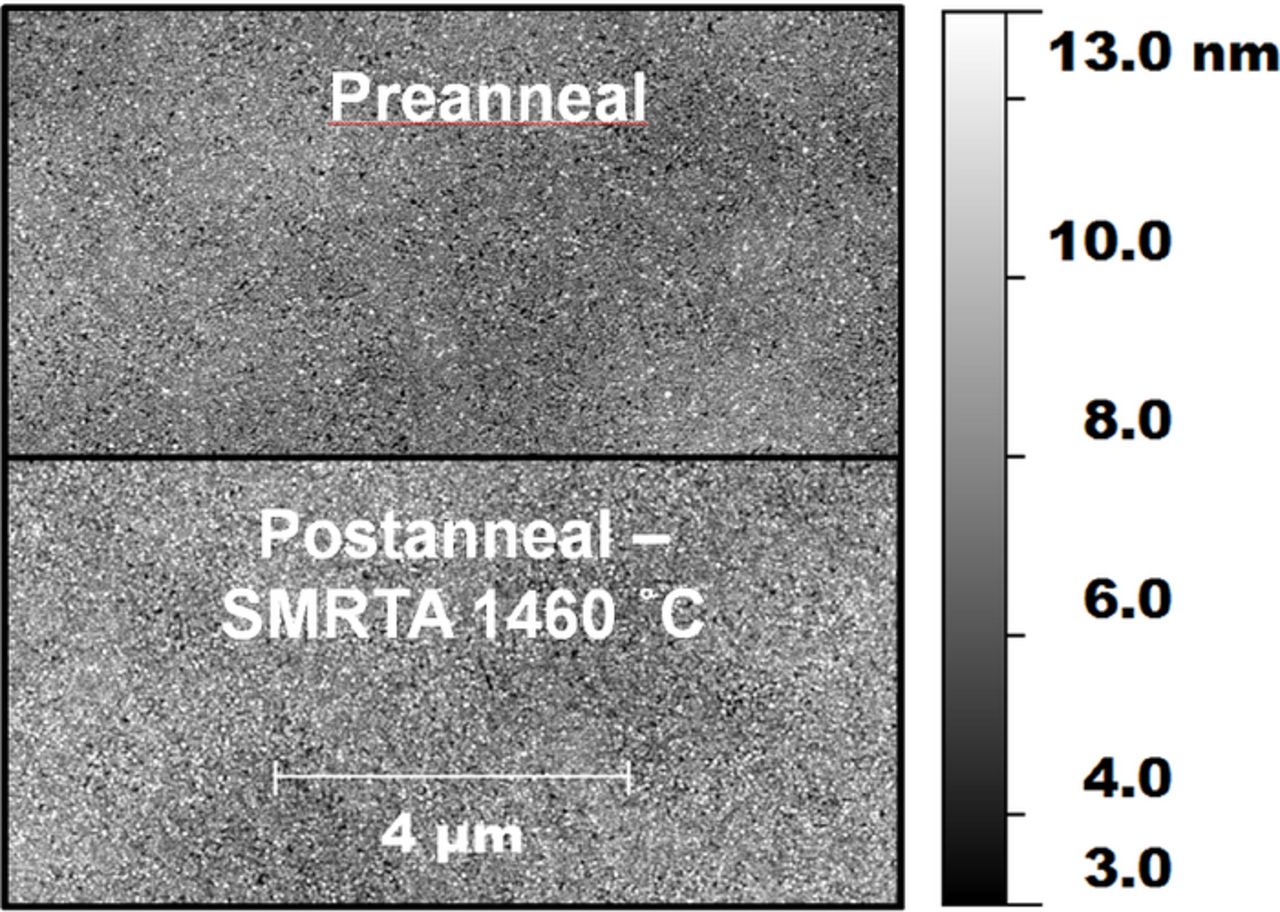
Figure 6. AFM image of the AlN-capped GaN before and after annealing using the SMRTA process at 1460°C. The RMS roughnesses before and after annealing are 1.55 and 1.65 nm, respectively.
To correlate electrical data with the structural improvements of the SMRTA process shown in experiments A and B, experiment C was conducted. The first sample in experiment C was annealed with the MRTA/1350/20 process while the second sample was annealed with the SMRTA/1350/20 process. The resistivity of the films were measured and compared as shown in Figure 7. The sample that was annealed with the MRTA/1350/20 process had a resistivity of 500 Ω·cm while the sample that was annealed with the SMRTA/1350/20 annealing process had a resistivity of 0.83 Ω·cm, as shown in Figure 7. This improvement in electrical conductivity is attributed to the removal of compensating defects during the additional conventional annealing step after the rapid heating pulses, which is consistent with the Raman spectroscopy results shown in Figs. 4 and 5.
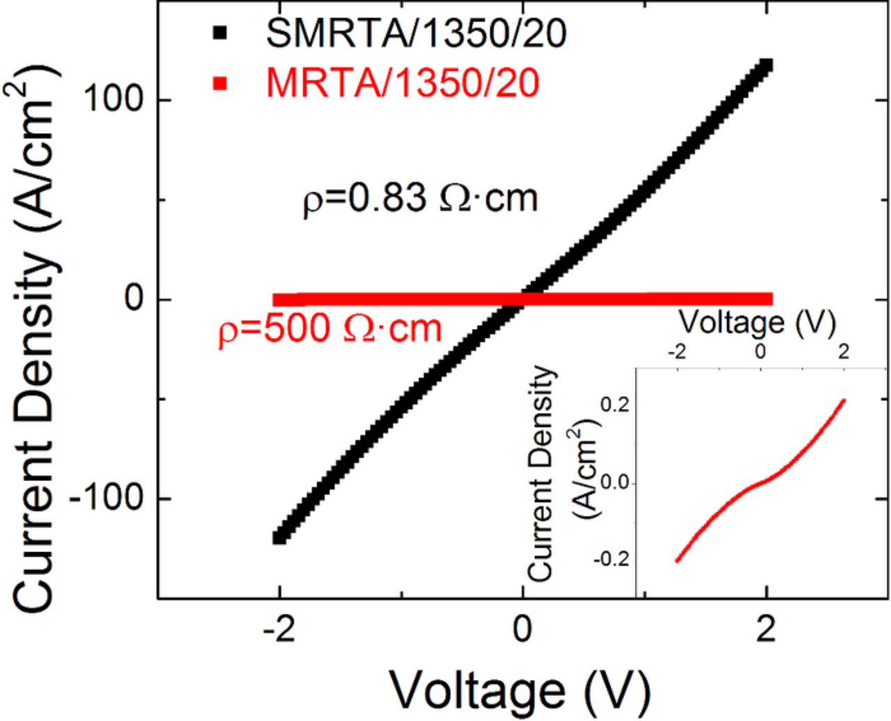
Figure 7. Current-Voltage curve for MRTA/1350/20 and SMRTA/1350/20 annealed samples. The sample annealed with the SMRTA process had a lower resistivity by nearly 3 orders of magnitude. This lower resistivity is attributed to the removal of compensating defects, confirming the Raman spectroscopy analysis in Figs. 3 and 4. The MRTA/1350/20 annealed sample I-V curve is shown in the inset. The SMRTA sample has a more linear I-V curve, indicating a better ohmic contact, which is consistent with lower levels of compensating defects.
To directly confirm p-type activation after Mg implantation, experiment (D) was conducted to form and characterize a p-i-n diode. The fabrication and characterization details of the p-i-n structure can be found elsewhere.25 The sample was processed using the SMRTA/1340/20 annealing process. Mg-implanted GaN p-i-n diodes have been previously demonstrated using a conventional annealing approach of 1230°C for 1 minute.26 However, the Mg ion dose and maximum energy utilized were 1 × 10¹⁴ atoms/cm2 and 60 keV, respectively.26 These lower energies and doses are expected to create less lattice damage and thus may not require the high annealing temperatures utilized in this research.27 The Mg-implanted PIN diode annealed using the SMRTA process exhibits rectifying behavior with a turn on voltage of ∼3 V as expected for the device structure as shown in Fig. 8. The formation of the rectifying junction by the SMRTA process demonstrates p-type activation of implanted Mg in a GaN device structure. This process can be utilized in devices that require selective area doping and will be a key enabling step for future power electronic devices.
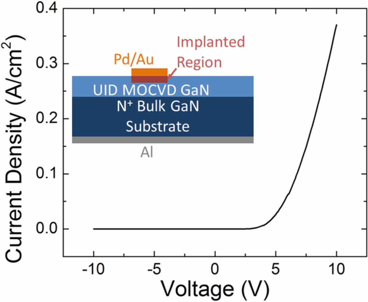
Figure 8. Current-voltage curve for the Mg-implanted p-i-n diode. The diode rectifies with a turn on voltage of ∼3 V as expected.
Conclusions
In summary, an improved annealing process, SMRTA, was demonstrated and characterized. The SMRTA annealing process included two conventional annealing steps at the beginning and end of the annealing process. Rapid heating and cooling cycles were performed in between these conventional annealing steps. Although the MRTA process enables the recovery of implantation-induced lattice damage, the rapid, pulsed thermal cycling also creates structural changes in the samples. It was shown that the additional post-pulse anneal in the SMRTA process reverses these changes and further improves the crystal structure of Mg implanted GaN. This was demonstrated by narrower Raman E2 FWHM modes as well as increased conductivity in the samples annealed with the SMRTA process compared to those annealed with the MRTA process. Furthermore, it was shown that the SMRTA process is capable of producing an Mg-implanted rectifying junction. The demonstration of this key enabling step will lead to selective area planar doping in GaN and thus transformative power electronic devices.