Abstract
We report a method for electrochemical roughening of thin-film platinum (Pt) electrodes that increases active surface area, decreases electrode impedance, increases charge injection capacity, increases sensitivity of biosensors and improves adhesion of electrochemically deposited films. First, a well-established technique for electrochemical roughening of thick Pt electrodes (wires and foils) by oxidation-reduction pulses was modified for use on thin-film Pt. Optimal roughening of thin-film Pt electrodes with this established protocol in a sulfuric acid solution was found to occur at about four times lower frequency than that typically used for thick Pt. This modification in established procedure created a 21x surface area increase but showed nanoscale cracks from inter-grain Pt dissolution that compromised film integrity. A crack free surface with Pt nanocrystal re-deposition (20–30 nm in size) and higher enhancement in surface area (44x) was obtained when the electrolyte was switched to a non-adsorbing perchloric acid solution. These electrochemically roughened electrodes have charge injection limits comparable to titanium nitride and just below carbon nanotube-based materials. Roughened microelectrodes showed a 2.8x increase in sensitivity to hydrogen peroxide detection, indicative of improved enzymatic biosensor performance. Platinum iridium and iridium oxide coatings on these roughened surfaces showed an improvement in adhesion.
Export citation and abstract BibTeX RIS

This is an open access article distributed under the terms of the Creative Commons Attribution Non-Commercial No Derivatives 4.0 License (CC BY-NC-ND, http://creativecommons.org/licenses/by-nc-nd/4.0/), which permits non-commercial reuse, distribution, and reproduction in any medium, provided the original work is not changed in any way and is properly cited. For permission for commercial reuse, please email: oa@electrochem.org.
Microfabrication techniques have enabled the bulk fabrication of robust, reproducible neural interfaces.1,2 These neural interfaces typically contain conductive metal electrodes that serve as the 'interface' between the device and the tissue.3 When microfabricated, these electrodes are typically thin films of metal, a few hundred nanometers thick and recent advances show these interfaces to be constructed on thin flexible substrates, further improving the ability of electrodes to interface with tissue.4–7 While these thin film electrodes generally act very similar to bulk metal found in non-microfabricated neural interfaces, they can be more delicate than bulk metal,8 especially when fabricated on a flexible substrate. Both bulk and thin film metal interfaces demand highest performance to ensure that they can properly interface with tissue without causing damage to the tissue. Often, electrode surface modifications are needed to enhance performance.
Enhanced electrode performance can be accomplished by 1) roughening the electrode surface to increase the effective surface area;9–11 or, 2) depositing a thin-film coating of a material with enhanced electrochemical activity.12–15 When depositing a different thin film electroactive material over the electrode to improve performance, there is often poor adhesion of the deposited film to the electrode surface.9,16 Poor film adhesion compromises the mechanical robustness of an implantable device which may result in immediate delamination or decreased lifetime of the electrode upon implantation, ultimately deteriorating sensor performance. While roughening the electrode surface can, by itself, improve electrode performance, it can also in many cases, improve the adhesion of coatings by increasing the contact area between the substrate and the coating.12,17 Here we examine the utility of a new technique to both 1) increase the active surface area of thin-film platinum (Pt) electrodes and 2) improve adhesion of electrodeposited coatings to thin-film Pt electrodes.
Several roughening methods can increase the effective surface area for certain electrode geometries, like roughening a planar electrode through some form of etching, e.g. by a plasma18 or laser etching.9 However, these methods require complex fabrication processes and costly equipment. Simpler, more affordable methods for roughening of thick metal and foil electrodes have also been tested. For example, an inexpensive wet chemistry technique for electrochemical roughening of thick metals was developed in 1973 when roughening of silver (Ag) foil electrodes allowed for the first observation of surface-enhanced Raman spectroscopy (SERS).19 The method was later developed for SERS on thick Pt samples.20 Additionally, platinum,10,11,20 gold,21 silver19 and palladium22 thick metal (wire and foil) electrodes can be roughened electrochemically with application of bipolar pulses that form oxides during anodic pulse and etch away those oxides during cathodic pulse. Roughening via electrochemical etching is attractive because it yields large increases in surface area with low cost, low toxicity, and well controlled processes. Platinum disk (foil or wire) electrodes have been electrochemically roughened and evaluated for use as neural stimulation electrodes.10,11 Roughening with a series of oxidation-reduction voltage pulses increased the active surface area up to 75x10 and was recently further optimized to achieve a 250x increase in surface area11 and led to increase in charge injection limit up to 1000 μC/cm2 (from 50−150 μC/cm2 for untreated Pt).11
The newest generation of neural interfaces requires further miniaturization to the microscale, with electrode surface areas of ≤8000 μm2 instead of larger macroscale electrodes (>49,000 μm2). Densely-packed microelectrodes in a region are preferred over a single macroelectrode to increase resolution and selectivity in both stimulating and recording electrical and chemical signals in neural interfaces of the future. Microelectrodes, when used for stimulation allow smaller, more specific activation of neuronal populations. When cell signals are recorded on microelectrodes, their geographical location can be more accurately pinpointed.
One consequence of this miniaturization, however, is a reduction in the geometric area of the electrodes. This reduction in geometric area can compromise important electroactive characteristics of the electrodes used for a wide range of biomedical applications. These compromised characteristics include 1) diminished charge that can be safely delivered by the electrode during neuro-stimulation,11 2) undesirable increases in impedance for recording electrodes,18,23 and 3) decreased signals for electrochemical biosensors.24 To develop devices with greater spatial resolution for these desired applications, while maintaining the same electroactive functionality, microelectrodes must have enhanced performance compared to the performance of macroelectrodes. To counteract the reduction in performance due to decreased geometric area, while still retaining the advantages of the microelectrodes, methods for increasing the surface area of the electrodes are required. Thin film microfabrication techniques are essential for this miniaturization. Due to the fragile nature of thin film, new methods must be developed to achieve this surface area enhancement without simultaneously destroying the electrode.
Here, we describe an electrochemical roughening process that enhances electrode performance and is non-damaging to thin-film Pt materials. We demonstrate that this process is applicable to thin-film electrodes with both macro and micro geometries despite differences in the electric field densities for the two geometries. And finally, electrodes roughened with this technique demonstrate enhanced adhesion of surface coatings and sensitivity for biosensing.
Experimental
Electrode and device fabrication
Commercial foil based macroelectrodes used in this study were 2 mm diameter Pt disk electrodes (CH Instruments, Inc., Austin, TX). The custom macroelectrode devices were microfabricated on a silicon substrate. The silicon substrate has a 0.5–1 μm thick layer of thermal oxide. Trace metal (Ti/Pt/Ti, 20 nm/250 nm/20 nm) was sputter-deposited on the wafers and patterned via photolithography and dry etching (Ar/Cl plasma). A 5 μm thick layer of polyimide (PI-2611, HD Microsystems) was then deposited on top of the wafer and patterned via photolithography and dry etching (O2 plasma) to define the electrode area and to act as an insulation layer. These Pt macroelectrodes are 1.2 mm diameter circles recessed from the surface of the polyimide.
Microelectrode arrays were fabricated using alternating stacks of metal (for the electrode and the trace metal layers) and polyimide (for the insulation layers). The electrode metal is sputter deposited platinum (250 nm thick) with a titanium adhesion layer (20 nm thick). 2 μm thick layers of polyimide (PI-2610, HD Microsystems) are used for the insulation layers. Additional details of the fabrication process used are outlined elsewhere.4,25 The Pt microelectrodes are 20 μm in diameter and flush with the surface of the polyimide. The custom macroelectrodes and the microelectrode arrays are fabricated using the same platinum source. Electrodes fabricated in house were also confirmed to have surfaces of pure Pt using energy dispersive x-ray analysis (EDX).
Electrochemical cell
All measurements in this paper including cyclic voltammetry (CV), impedance, voltage transients, roughening, film depositions, and potential cycling for adhesion tests were performed in a 3-electrode cell and all potentials are given with respect to Ag|AgCl electrode unless otherwise noted. A Pt wire was used as a counter electrode. To avoid alterations to the Pt oxidation process due to chloride ion contamination, a leakless Ag|AgCl reference electrode (ET069-1, eDAQ Company, Australia) was used for all electrochemical tests.
Pretreatment before tests
Pt disk electrodes were re-polished before each roughening test with each of the following for 1 minute each: 15, 3 and then 1 μm diamond polish solution (PK-4 Polishing Kit, product of BASi, West Lafayette, IN). Pt thin-film electrodes were soaked in acetone for 30 minutes prior to tests to remove adsorbed organics from the surface of the electrodes. All electrode surfaces were electrochemically cleaned in sulfuric acid (H2SO4) or perchloric acid (HClO4) (0.5 M concentration; 99.999% purity solutions) by 50–200 repeated CV cycles (0.25/1.25 V at 0.2V/s scan rate) before testing.
Electrochemical roughening procedures
A VersaSTAT 4 Potentiostat (AMETEK Inc., Berwyn, PA) was used for electrochemical roughening procedures. Roughening of disk electrodes and thin film macroelectrodes was performed in aqueous solutions of H2SO4 or HClO4 (0.5 M concentration; 99.999% purity) by applying a train of pulses with 1.9–2.65 V oxidation pulse amplitude and −0.15 V reduction pulse amplitude for 100–300 s followed by a −0.15 V potentiostatic reduction for 4 minutes. Pulsing frequency was varied sample to sample in a range of 250–4000 Hz. Microelectrodes were roughened in an aqueous solution of HClO4 (0.5 M concentration; 99.999% purity) by applying trains of pulses with 1.2–1.4 V oxidation pulse amplitude and −0.25 V reduction pulse amplitude for 100 s at 4000 Hz with a duty cycle of 1:3 (oxidation to reduction pulse width) followed by a −0.2 V potentiostatic reduction for 3 minutes.
Electrochemical characterization methods
Effective surface area and roughness factor estimation
Surface roughness was assessed using electrochemical methods and top down scanning electron microscopy (SEM). Effective surface area of untreated and roughened macroelectrodes was determined from the hydrogen adsorption peaks during cyclic voltammetry in 0.5 M H2SO4 (or 0.5 M HClO4 for samples roughened in this solution) according to the method outlined by J. Rodríguez, et al.26 Effective surface area of microelectrodes was determined from the double layer capacitance values obtained during electrochemical impedance spectroscopy, since hydrogen adsorption peaks were poorly resolved in microelectrode CVs.26 Roughness factor is defined as the ratio of the effective (active) surface area to the geometric area.
Electrochemical impedance spectroscopy measurement and modeling
Impedance spectra were measured under open circuit conditions in phosphate-buffered saline (PBS, not de-aerated) (30mS/cm conductivity; pH 7) with 10 mV amplitude sine wave applied over a frequency range (1 Hz–100 kHz) with a SP-200 Potentiostat (Bio-Logic Science Instruments, France). Spectra were fitted using EC-Lab Software (Bio-Logic Science Instruments, France) with an equivalent circuit model.
Voltage transient measurement and data analysis
Voltage transients were measured in PBS (not de-aerated) with PARSTAT 3000A Potentiostat (30V polarization capabilities; AMETEK Inc., Berwyn, PA) as a response to a biphasic current pulse waveform with 20–30 μs interpulse delay. Polarization potentials were extracted from a potential measured at the interpulse step using the graphical method of Cogan and colleagues.23
Film deposition for adhesion lifetime testing
Platinum iridium (PtIr) (60:40 alloy) film deposition was conducted using a procedure adapted from Petrossians et al.27 Briefly, the plating solution consisted of sodium hexachloroiridate (III) hydrate (0.2 g/L) and sodium hexachloroplatinate (IV) hexahydrate (0.186 g/L) dissolved in 0.1 M nitric acid. PtIr films were deposited at room temperature on the microelectrodes with 800 repetitive potential cycles from −0.1 to 0.1 V at a 0.5 V/s scan rate. PtIr deposition on the microelectrodes was visually confirmed after deposition.
Iridium oxide (IrOx) film deposition was conducted using the procedure outlined by Yamanaka, et al.28 Briefly, iridium chlorohydrate (30 mg) was added to 20 mL DI water and dissolved by stirring for 30 min. Then, H2O2 (0.2 mL, 30%) was added and stirred for 10 minutes in a closed container. Oxalic acid (100mg) was added and stirred for another 10 minutes until dissolved. Potassium carbonate was added to the solution until the pH was 10.5. The solution was aged at room temperature for 2–5 days until the iridium(III) was fully stabilized as iridium(IV) oxalate in the solution (indicated by color change to dark purple); it was then transferred to a refrigerator for storage. Films were deposited on the microelectrodes with 200–350 repetitive CVs from 0 V to 0.6 V at a 50 mV/s scan rate. IrOx deposition was visually confirmed on the microelectrodes after deposition.
Adhesion of the electrodeposited coatings on microelectrodes was tested only by electrochemical means with repetitive redox cycling as outlined by Boehler et al.16 and Petrossians et al.27 For this test of PtIr and IrOx electrodeposited films, electrodes were subjected to CVs from −0.6 V to 0.9 V at a scan rate of 0.5 V/s based on parameters employed by Petrossians et al.27 Visual inspections of the film for cracking and delamination occurred every ∼20 CVs. Electrochemical impedance was also periodically measured for each electrode. The results from the films deposited on the roughened electrodes were compared to those deposited on non-roughened electrodes.
Biosensor performance tests
Sensitivity to H2O2 was used as an indicator of the ability of the electrodes to act as biosensors. Sensitivity to H2O2 was determined by measuring the current in PBS with the microelectrodes held at 0.7 V. Increasing concentrations of H2O2 (30% stock, KMG Electronic Chemicals, Inc., Fort Worth, TX) were added. Final H2O2 concentrations in PBS were measured from about 1 μM to 30 μM. The slope of the current response versus H2O2 concentration was calculated per unit area, yielding the sensitivity.
Surface morphology characterization
Microscopy images were taken using a Keyence VHX Digital Microscope with VH-Z250R Real Zoom lens. The scanning electron microscope images were collected in a JEOL-JSM-7401F field emission SEM.
Results and Discussion
Influence of electrochemical parameters on roughened film quality
For thin-film Pt macroelectrodes, the roughening protocol for Pt wires in 0.5 M H2SO4 from Weremfo, et al.11 resulted in film delamination (1 kHz pulsing −0.4/2.4 V vs Ag|Ag2SO4|sat K2SO4 [−0.15/2.65 V vs Ag|AgCl] for 100 s followed by −0.4 V reduction until oxide is completely reduced). Decreasing the positive pulse amplitude to 2.2 V (−0.15/2.2 V amplitude, 1 kHz frequency, 100 s duration) still led to film delamination (see Figure 1a for representative image). Further decreases in voltage amplitude to 2.1 V (−0.15/2.1 V, 1 kHz frequency, 100 s duration) did not cause any delamination of the film but also caused no roughening of the electrode surface (no differences seen in cyclic voltammetry before and after roughening). Attempts to modulate the pulse frequency were more successful in creating roughened films, demonstrating that thin film roughening without visible film delamination can be achieved with a decreased oxidation-reduction pulse. Thin-film macroelectrodes roughened at 250 Hz for 100 s with a 2.2 V positive pulse amplitude show uniform roughening (see Figure 1b for representative image) that increases the active area 13x.
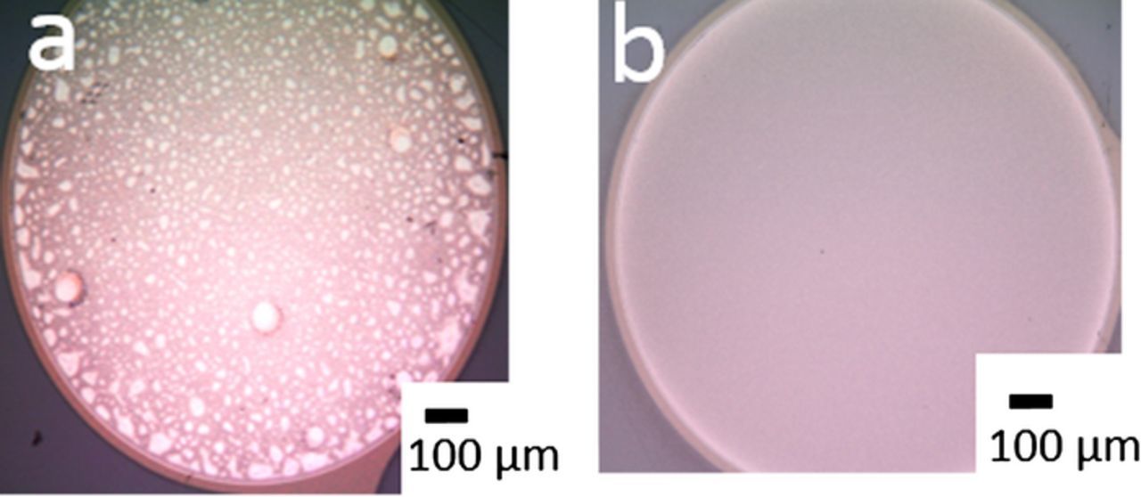
Figure 1. Thin film Pt macroelectrodes roughened in H2SO4 solution (a) with −0.15/2.2 V pulsing at 1 kHz for 100 s and (b) with −0.15/1.9 V pulsing at 250 Hz for 100 s. The higher pulse frequency of 1 kHz resulted in delamination of the film, whereas pulsing at the lower frequency of 250 Hz roughened the film with no delamination.
To examine the frequency dependence for roughening of both thick (Pt disks) and thin films, Pt disks (foils) and thin-film Pt macroelectrodes were roughened over a range of frequencies (150 to 4000 Hz) with all other parameters fixed (−0.15/1.9 V pulsing for 100 s followed by a potentiostatic reduction). Roughness factors shown in Figure 2 indicate that optimal frequencies for roughening exist and that these frequencies are different for thin-film and thick Pt. Optimal frequencies for the roughening of the thick, Pt disks are 1–2 kHz, in agreement with previously published results11,20 while the optimal frequencies for roughening the thin-film Pt macroelectrodes are in the range of 250–350 Hz. Successful roughening of thin-film Pt was only observed in the frequency range 150–500 Hz.

Figure 2. Effect of pulse frequency on roughness factor for representative Pt foil (blue) or thin-film Pt (red) macroelectrodes. All roughening occurs in H2SO4 with −0.15/1.9 V pulsing for 100 s. Reproducibility of surface area increase for samples roughened under identical pulsing parameters was within 10%.
Several factors likely contribute to the frequency dependence of pulsed roughening. The roughening process is controlled by the rates of oxide formation and reduction that occur during each pulse. The chemistry of oxide formation on Pt is complex and involves stages of oxygen species adsorption, progressive oxidation with reversible and irreversible steps, oxygen species diffusion and surface reconstruction.29,30 Short (too high frequency) pulses are inefficient since they only drive double layer charging and initial reversible stages of surface oxide formation that lead to roughening but do not leave time for oxide diffusion and surface reconstruction before oxide reduction. Longer pulses (too low frequency) are inefficient as well due to diffusion limitations that lead to current decay within a pulse. Examination of the surface morphology of roughened Pt provides further insight into factors that influence the ideal frequency range for roughening of foils and thin films.
To examine the surface morphology of electrodes roughened with this technique, the roughened thin-film Pt (1.9/−0.15 V, 250 Hz, 200-second-long pulsing) that resulted in the highest (21x) surface area increase without film delamination was examined by SEM. Comparison of SEM images of untreated (Figure 3a) and roughened (Figure 3b) films reveals nano-scale cracking and dissolution at grain boundaries in the roughened surface (Figure 3b). This indicates that oxide dissolution occurs preferentially at grain boundaries rather than at the grains in the Pt thin films. Therefore, we propose that the altered frequency response for roughening of thin films compared to foils results from different reactivity at grain boundaries rather than grains. Although synthesis or structure information are not available for disk electrodes used in this study, foils and wires are typically synthesized at higher temperature than sputtered films. This may influence diffusivity of oxygen species at inter-grain boundary material controlling the timescale of the reactions.
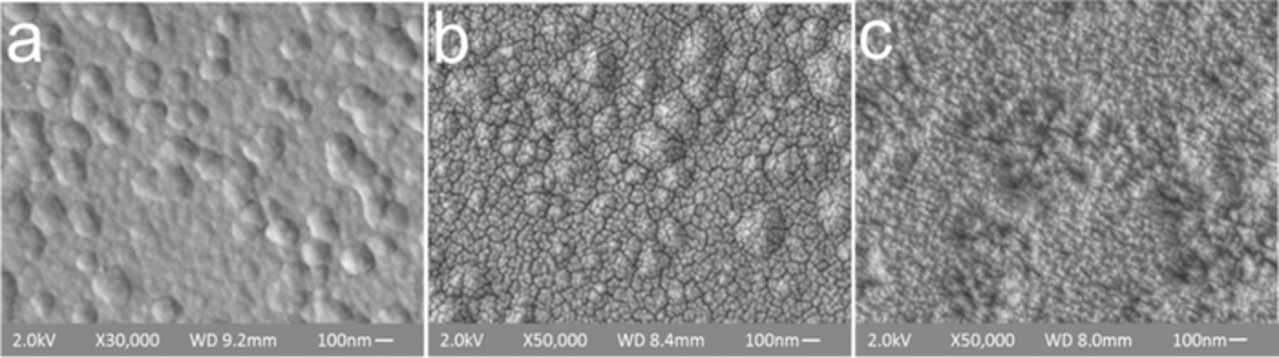
Figure 3. SEM of thin film macroelectrodes (a) Untreated; (b) after roughening in 0.5 M H2SO4 with −0.15/1.9 V 250 Hz 200 s pulsing (resulting in a 21x area increase) and (c) after roughening in 0.5 M HClO4 with −0.15/1.9 V 250 Hz 300s pulsing (resulting in a 44x area increase).
Greater reactivity at grain boundaries of polycrystalline Pt in H2SO4 has been reported previously for the Fe2+/Fe3+ redox reaction due to adsorption of the sulfuric acid anion blocking grain reactivity.31 Interestingly, in previous work grain boundary preferential reactivity was eliminated when the reaction occurred in the less adsorptive perchloric acid (HClO4). Since cracking is an undesirable change in electrode morphology with the potential to compromise film integrity, the roughening experiments were continued in the less adsorptive electrolyte, HClO4.
A larger surface area increase, with no detected grain boundary dissolution, is achieved by switching from the adsorptive H2SO4 to the less-adsorptive HClO4 solution. In HClO4, optimized pulsing parameters (1.9/−0.15 V, 250 Hz 300s pulsing) resulted in a 44x increase in electrode surface area with no visual delamination or dissolution at the grain boundaries observed (n = 1). Examination of the roughened film morphology with SEM revealed that roughening in HClO4 occurs without cracking and with re-deposition of 20–30 nm Pt crystals (Figure 3c). This may explain the greater increase in surface area, compared to roughening in H2SO4. The surface area increase for samples roughened under identical pulsing parameters was consistently reproducible with <10% variation in resulting roughness factor. Optimal roughening frequencies in HClO4 solutions were in the same range as optimal frequencies observed in H2SO4 solution (as shown on Figure S1a).
To determine the neural recording capabilities of these nano-roughened electrodes, thin-film Pt macroelectrodes were roughened in 0.5 M HClO4 with varied pulsing duration, pulse frequency, and oxidative pulse amplitude. Varying these parameters resulted in 5–40x increases in active surface area (Table I). Untreated and roughened electrodes were further characterized by recording impedance spectra and voltage transients as a response to current pulses in PBS solution (Table I and Figure 4a). Roughening parameters included: pulse frequency (F), pulse duration (T), and oxidation pulse amplitude (V). Reduction pulse amplitude was −0.15 V for all tests. The roughness factor was calculated from the CV. Measured impedance spectra showed linear Nyquist plots with no bending (Figure S1b), indicating absence of charge transfer due to sluggish kinetics of dissolved oxygen reduction. For data analysis, curves were fitted with equivalent circuit model Rohm+ CPE, where Rohm is the ohmic resistance (composed of the device trace electrical resistance and ionic resistance of the solution Rohm = Rtrace + Rsolution) and CPE is the constant phase element representing the double layer capacitance at the electrode-solution interface. A representative Nyquist plot for a roughened electrode with data fit using Rohm + CPE equivalent circuit model is shown in Figure S1b. The constant phase element (CPE) parameters of double layer capacitance (Q) and exponent (α) were extracted from fitting EIS spectra with an equivalent circuit model. Also shown is the magnitude of the impedance (|Z|) at 1kHz.
Table I. Summary of surface characteristics for macroelectrodes roughened in HClO4.
| Roughening parameters | Surface Characterization | ||||||
|---|---|---|---|---|---|---|---|
| Treatment | F (Hz) | T (s) | V (V) | Roughness factor | Q (mF/sα-1 cm2) | α | |Z| at 1kHz (Ohm) |
| Untreated | NA | NA | NA | 0.8 | 0.05 | 0.94 | 672 |
| Roughened | 200 | 10 | 2.1 | 4.8 | 0.45 | 0.95 | 340 |
| Roughened | 100 | 50 | 2.1 | 14.8 | 0.86 | 0.94 | 361 |
| Roughened | 200 | 50 | 2.1 | 21.5 | 1.27 | 0.94 | 349 |
| Roughened | 100 | 200 | 2.0 | 31.1 | 1.70 | 0.93 | 350 |
| Roughened | 200 | 100 | 2.1 | 40.0 | 1.99 | 0.93 | 344 |
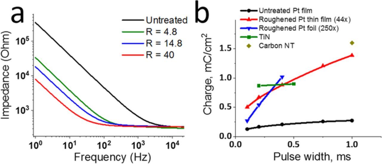
Figure 4. Recording and stimulation characteristics of the roughened films: (a) impedance spectroscopy in PBS for untreated and roughened thin-film electrodes with various surface area increases (R); and (b) charge injection limits for untreated and roughened thin-film Pt roughened to 44x area increase, n = 1 electrode for each data point. Also shown for comparison are the performance of other materials extracted from literature.36,37
As the double layer capacitance increases for the roughened electrodes, the absolute impedance values decrease by more than an order of magnitude at low frequencies (1–100 Hz). In addition, the absolute impedance approaches the lower limit of ohmic resistance (Rohm) at the biologically relevant frequencies for monitoring single neuron activity (∼1 kHz) (Figure 4a). Double layer capacitance (Q) values reported in Table I were determined by fitting impedance spectra with a monotonic equivalent circuit model (see Experimental section for details). There is a nearly linear increase in Q from 0.05 mF/sα-1 cm2 for untreated Pt to 2 mF/sα-1 cm2 for the maximum roughened Pt thin-film; this 40x increase in Q corresponds with the 40x increase in surface area (Table I). The Q value reported here for untreated Pt (50 μF/ sα-1 cm2) is in good agreement with the range (10–60 μF/cm2) typically observed on smooth metal electrodes in similar tests.32 The double layer capacitance of our roughened thin film electrodes (2 mF/sα-1 cm2) is comparable to the electrodes roughened to a similar surface area by Weremfo, et al.11 and to deposited PtIr alloy films27 both of which are commonly used as stimulation and recording electrode material on neural interfaces.
To determine macroelectrode neural stimulation capabilities, charge injection limits of untreated and roughened thin-film Pt electrodes were measured by recording the voltage transient responses to biphasic current pulses of increasing amplitudes until a safe threshold of −0.6 V was observed at an intermediate step (Supplemental Figures S2a–S2b). At the roughened thin film electrodes charge injection occurs through a combination of non-faradaic double layer charging and faradaic electron-transfer processes common for Pt electrodes.33 In addition, reduction of dissolved oxygen in the PBS solution during measurements is also contributing to charge injection during current pulses. Untreated thin-film electrodes reached threshold at 0.17 mC/cm2 charge per phase with 0.2 ms pulses and at 0.26–0.27 mC/cm2 with longer pulses (0.75–1 ms) (Figure 4b). These values are in good agreement with the reported charge injection limits for untreated Pt: with 50–150 μC/cm2 for short 0.2 ms pulses34 and 0.3–0.35 mC/cm2 for longer ms range pulses.35 Roughened electrodes with a 44x increase in surface area showed 2–4 times greater charge injection limits (0.5–1.39 mC/cm2) as compared to the untreated samples, Figure 4b, Supplemental Figures S2c–S2d). For reference, charge injection limits for carbon nanotube array electrodes,36 titanium nitride electrodes37 and thick Pt roughened with a 250x area increase were extracted from literature and added to Figure 4b. Roughened thin-films have greater charge injection limits than laser roughened Pt foil electrodes (∼0.2 mC/cm2 for pulse widths 0.8–1 ms),9 comparable charge injection limits to TiN37 (Figure 4b) and limits just below carbon nanotube-based material (Figure 4b).36 Surprisingly, despite the lower achieved roughness, thin-film Pt roughened with a 44x area increase had greater charge injection limits than the thick Pt roughened with 250x area increase for pulse widths below 0.3 ms. This improvement may originate from the differences in surface morphology that could favor interfacial charge transfer at the thin-film electrode with nano-crystallites compared to a thick electrode with nano- or micro-porosity.
Roughening microelectrodes
Microelectrodes (20 μm diameter) were roughened with pulsing in 0.5 M HClO4 with oxidation pulse amplitudes ranging from 1.2 to 1.4 V and constant −0.25 V reduction. CVs measured in HClO4 solution indicate increased current after roughening (Figure S3a). Since hydrogen adsorption peaks were not well resolved on microelectrode CVs, surface area increase was estimated from analysis of impedance spectra instead of hydrogen adsorption using cyclic voltammetry.26 SEM analysis confirmed the electrode surfaces were roughened, with no signs of cracking or delamination, and showed the same crystal re-deposition with larger crystals (up to 100–200 nm in size) observed on the macroelectrodes (Figure 5). Both size and density of crystals increased with larger oxidation pulse amplitude (up to 200 nm in size for −0.25/1.4 V pulsing on Figures 5c and 5f).
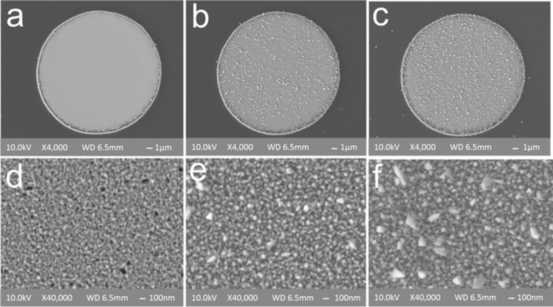
Figure 5. SEM of microelectrode surfaces roughened at different pulse amplitudes: (a) and (d) −0.25/1.25 V; (b) and (e) −0.25/1.35 V; (c) and (f) −0.25/1.4 V for 100 s. Increased size and number/density of re-deposited Pt crystals is observed with increasing oxidation pulse amplitude. No cracking or delamination of the films was observed.
Impedance spectroscopy in PBS was performed on the microelectrodes before and after roughening. Impedance noticeably decreased after roughening for all oxidation pulse amplitudes tested (Figure 6a). Impedance spectra were fit with an equivalent circuit model (see Experimental section for details) and Q was extracted and plotted as a function of oxidation pulse amplitude. As with the macroelectrodes, roughening increases with Q proportionally with pulse amplitude (Figure 6b). Up to a 2.7x area increase was achieved for samples roughened under 1.4V pulse amplitude. Smaller increases in surface area after roughening, compared to those observed in the macroelectrodes, may originate from the increased electric fields experienced by the flush microelectrodes under electrochemical processes in comparison to the recessed macroelectrodes.
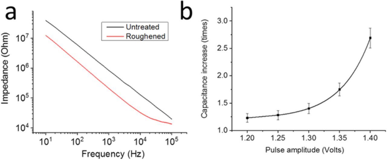
Figure 6. Impedance characteristics of roughened microelectrodes: (a) Representative impedance spectra before (black) and after (red) roughening at −0.25/1.4 V pulsing; (b) Relative increase in double layer capacitance (Q) after roughening as a function of oxidation pulse amplitude during roughening (n = 3). Error bars indicate standard deviation.
Improving adhesion of thin-film coatings by roughening pretreatment
Platinum iridium coating
The adhesion of PtIr to roughened (n = 17) and untreated (n = 14) Pt microelectrodes (20 μm diameter) was examined. Electrodes were roughened with different oxidation pulse amplitudes (1.2–1.4 V) using the roughening procedure outlined above. PtIr was electrodeposited (see Experimental section for details) on these roughened microelectrodes, as well as untreated microelectrodes. After PtIr electrodeposition, all microelectrodes were put through repetitive potential cycling (see Experimental section for details; CV in PBS shown in Figure S3b) as a test of adhesion lifetime. 82% of the PtIr coatings deposited on untreated Pt surfaces (14 out of 17) delaminated after the first series of 20 potential cycles (Supplemental Figures S4 and S5). The remaining 18% of coatings on untreated Pt (3 out of 17) showed signs of degradation after the first 20 potential cycles, but not delamination. For the PtIr coatings deposited on roughened substrates, electrodes roughened at oxidation pulse amplitudes of 1.35 and 1.4 V did not show the same degradation after 1500 potential cycles were applied. Pictures of the PtIr coatings taken before and after 1500 potential cycles are shown in Supplemental Figure S5.
The electrochemical impedance at 1 kHz was recorded during adhesion testing as shown in Figure 7a. All samples showed an initial "activation" with an average 3.2x decrease in impedance (at 1 kHz) occurring during the first 20 potential cycles for all microelectrodes coated with PtIr. This activation effect may be related to irreversible roughening of the PtIr caused by initial dissolution of any loosely adhered deposits or to oxidation of the iridium during the initial cycles that stops after a thermodynamically stable oxide layer is formed. Impedance of the PtIr deposited on the roughened microelectrodes remained low (and stable after initial activation) for all microelectrodes, regardless of the oxidation pulse amplitude used for roughening.
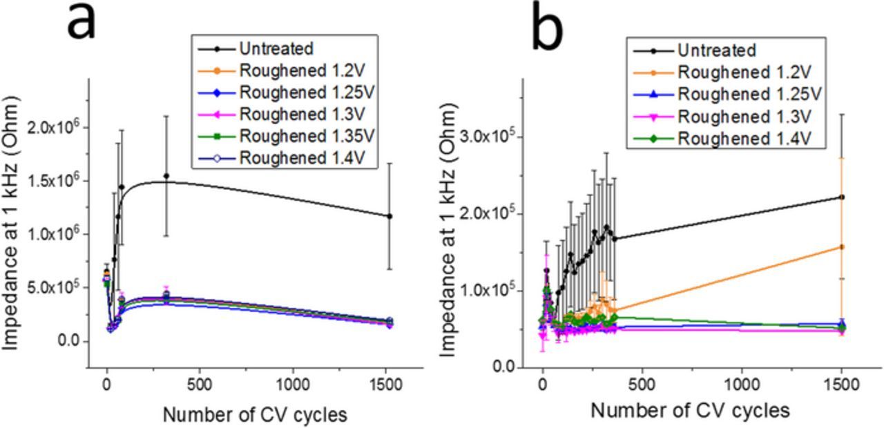
Figure 7. Tracking impedance at 1 kHz over 1500 cycles. (a) PtIr coatings deposited on untreated microelectrodes and microelectrodes roughened at different oxidation pulse amplitudes; (b) IrOx coatings deposited on untreated microelectrodes and microelectrodes roughened at different oxidation pulse amplitudes. Each data point contains data from a minimum of n = 3 microelectrodes. Error bars indicate standard deviation.
Iridium oxide coating
The adhesion of IrOx coatings was also examined on the microelectrodes (both untreated and roughened) (see Experimental section for details; CV in PBS shown on Figure S3b). Tests compared the lifetime of the IrOx coatings deposited on untreated microelectrodes (n = 8) and microelectrodes roughened using the procedure outlined above at different oxidation pulse amplitudes (1.2–1.4 V, n = 14). IrOx deposition was continued until the microelectrodes appeared blue under the microscope, typically requiring 200 cycles for untreated microelectrodes. However, due to the increased surface area, 350 deposition cycles were required on roughened microelectrodes to deposit an IrOx layer thick enough to display the characteristic IrOx blue color upon visual inspection. Three untreated microelectrodes were also coated with the thicker layer of IrOx (350 cycles), while five untreated microelectrodes had the 200-cycle deposition thickness. Images of the microelectrodes were taken before and after a total of 1500 potential cycles were applied (Supplemental Figure S5).
Most of the IrOx coatings deposited on the untreated microelectrodes (75%) showed visible signs of failure (e.g. delamination, cracking) after 1500 cycles. In contrast, only 14% of the IrOx coatings on the roughened microelectrodes showed failure after 1500 cycles. The only two roughened microelectrodes that showed delamination and/or cracking, like the untreated microelectrodes, were roughened with an oxidation pulse amplitude of 1.20 V, indicating that oxidation pulse amplitudes greater than 1.25 V were sufficient for improved adhesion of an electroplated IrOx film. As seen in Figure 7b, the untreated IrOx coated microelectrodes show noteworthy increases in impedance over the course of the 1500 potential cycles applied. This increase in impedance is a quantitative measure of the damage to the IrOx coating on an electrochemical level. Two IrOx coated, untreated microelectrodes did not show significant visual damage (Supplemental Figure S6) and still have lower impedances after 1500 CVs, contributing to the large error bars seen for this experimental group (Figure 7b). Similarly, the impedance of the IrOx coated, roughened microelectrodes stays relatively stable throughout the lifetime testing up to 1500 cycles. The two samples showing an increase in impedance (and thus, signs of damage on an electrochemical level) are correlated to the two microelectrodes roughened at 1.20 V that showed visual signs of failure after 1500 cycles. These quantitative measurements indicate improved adhesion of IrOx films on microelectrodes that are roughened at an oxidation pulse amplitude of at least 1.25 V.
Improving sensitivity of biosensor by surface roughening
The signals from chemical biosensors are also often proportional to the active surface area of the sensing electrode. One subtype of chemical sensors, enzymatic amperometric sensors, rely on the production and subsequent detection of hydrogen peroxide (H2O2) within the sensor.38 As the footprint of the sensor decreases, the number of H2O2 molecules detected must be maximized to improve sensor performance and one approach to improving this detection is increasing the active surface area of the sensor. To test the sensitivity of the roughened microelectrodes for biosensing applications, Pt microelectrodes were roughened using the procedure outlined above with a range of oxidation pulse amplitudes (1.2–1.4 V). To test the potential of the roughened microelectrodes to act as an enzymatic biosensor, sensitivity to H2O2 was measured as a proxy for sensor performance (e.g. glucose sensitivity on a device with immobilized glucose oxidase). Glucose sensors involve the incorporation of glucose oxidase onto the microelectrode surface, where H2O2 is generated from the interaction of glucose and glucose oxidase.39 The microelectrode detects H2O2 via oxidation on the surface of the electrode that causes an increase in current. Testing consisted of measuring the sensitivity of both roughened and untreated microelectrodes to H2O2 (see Experimental section for details); the slope of the relationship between the measured current and the total H2O2 concentration is then measured. This slope, normalized to the geometric area, is the sensitivity of the microelectrode to H2O2. An example of the calibration plot, in which current is measured as a function of time, can be found in the Supplementary Information (Figure S7). In PBS, the H2O2 sensitivity of untreated and roughened microelectrodes was tested over the range of 1–29.3 μM H2O2. Figure 8 demonstrates that all roughened Pt microelectrodes, regardless of the roughening oxidation pulse amplitude, exhibited higher sensitivity to H2O2 compared to untreated Pt microelectrodes. Increasing sensitivity to H2O2 plateaus at 1.3 V roughening oxidation pulse amplitude, after which additional surface area increases (i.e. higher oxidation pulse amplitudes) do not significantly increase H2O2 sensitivity. Roughened microelectrodes show more than double the H2O2 sensitivity of untreated microelectrodes, showing the promise of this roughening procedure for improved biosensor performance.
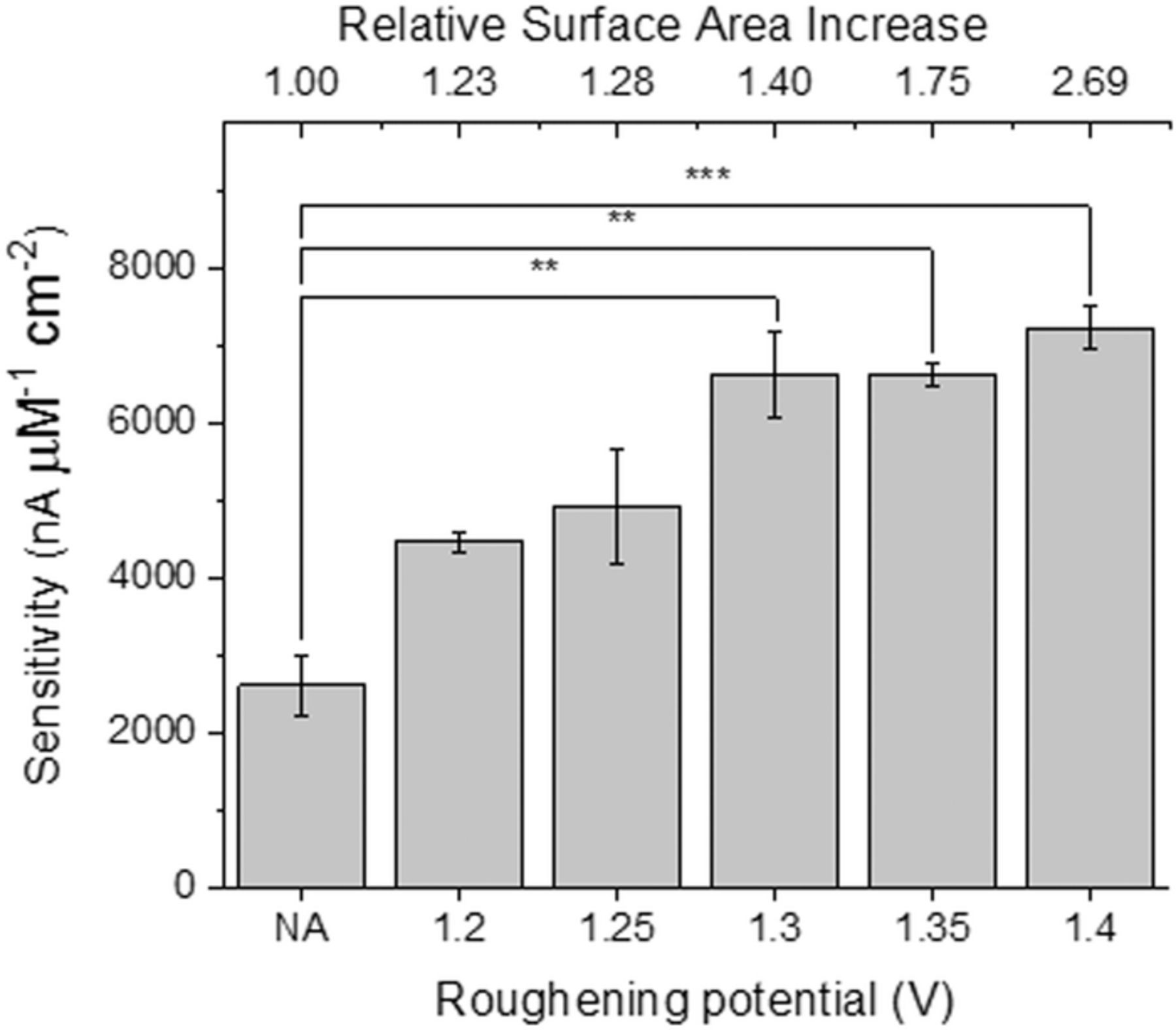
Figure 8. A comparison of average H2O2 sensitivity (in pA μM−1 cm−2) for different roughening oxidation pulse amplitudes (shown at the bottom) with the corresponding relative surface area increases shown at top of graph: Untreated (n = 7), 1.2 V (n = 6), 1.25 V (n = 5), 1.3 V (n = 6), 1.35 V (n = 7), 1.4 V (n = 6). Error bars indicate standard error of the mean. Asterisks (*) indicate significance in one-way ANOVA with Dunn's multiple comparisons post-test. **p ≤ 0.01, ***p ≤ 0.001.
Conclusions
Electrochemical roughening via oxidation-reduction pulsing can be used for non-destructive roughening of thin-film Pt macroelectrodes and microelectrodes. Roughening in the non-adsorbing electrolyte HClO4 provides higher surface area increases and less interface damage than roughening in the adsorbing electrolyte, H2SO4. Roughening treatments in HClO4 resulted in a crack free surface with Pt nanocrystal re-deposition and up to 44x enhancement in surface area on 250 nm thick Pt macroelectrodes. This roughening technique also non-destructively roughens microelectrodes but with a reduced enhancement in surface area before damage is seen. Roughening of 250 nm thick microelectrodes resulted in a 2.7x surface area increase with crystal re-deposition and no signs of film damage. This reduction in surface area is likely due to differences in electric field density and its effect on oxide formation, removal and re-deposition between the recessed macroelectrodes and flush microelectrodes.
Electrochemical roughening results in substantially enhanced electrode performance for both stimulation and recording. Improved recording capabilities on the thin-film, roughened, Pt macroelectrodes were observed as a 40x increase in interfacial double layer capacitance. These roughened electrodes had a 4–5x increase in the charge injection limits (i.e. stimulation capability) compared to untreated Pt. These increased charge injection limits are comparable to those seen for TiN, a commonly used stimulating electrode material.37
Coating adhesion tests showed significant improvement in PtIr and IrOx film lifetimes when deposited on roughened microelectrodes. During lifetime tests of PtIr, 82% of the films deposited on untreated Pt surfaces delaminated after several initial potential cycles while all the films deposited on electrodes roughened at potentials above 1.35 V survived 1500 potential cycles. During lifetime tests of IrOx, 75% of the films deposited on untreated electrodes showed visual signs of failure and increased in impedance after 1500 cycles. Roughening voltages of 1.25 V or above were sufficient to improve adhesion of IrOx film with no observed signs of degradation by EIS or microscopy after the complete series of 1500 cycles. In addition, roughened microelectrodes showed a 2.8x increase in H2O2 sensitivity for improved enzymatic biosensors. Based on these results, for biosensing and film deposition 1.35 V appears to be the optimal roughening voltage to use for greatest adhesion and sensitivity benefits.
We demonstrate a reliable roughening technique for thin-film Pt electrodes that maintains the integrity of the electrode interface while still enhancing their performance. This roughening technique improves the electrical recording, stimulation and biosensing performance of the thin-film electrodes and improves the adhesion of deposited electroactive coatings. These enhancements in electrode performance are critical as neural interfaces and their electrodes continue to miniaturize.
Acknowledgments
Professor Loren Frank is kindly acknowledged for his collaborations with the group that have enabled fabrication and design of the thin-film Pt microarrays discussed in the above work. This work was performed under the auspices of the U.S. Department of Energy by Lawrence Livermore National Laboratory under Contract DE-AC52-07NA27344 and funded by Lab Directed Research and Development Award 16-ERD-035. LLNL IM release #LLNL-JRNL-746398. Notes: Patent application on this work was filed on June 6, 2017, as application number 15/615,648. The application has also been published (US 2017 0350034). The authors declare no competing financial interests.
ORCID
Anna M. Belle 0000-0003-4044-635X
Allison Yorita 0000-0002-1267-8391