Abstract
Controlled transport of electrons through tunnel junctions and their confinement by mesoscopic structures have opened up immense possibilities of single-electron device (SED) applications. The realization of a practical working SED has remained challenging largely owing to the poor understanding of the physics of operation of singe-electron tunneling devices, especially of those with multiple nanometer-sized islands. In this simulation study of one-dimensional (1D) multi-island chains, we propose physical mechanisms that lead to the coulomb blockade (CB) and coulomb staircase (CS) characteristics that are enhanced by the geometrical disorder in the chain. With increasing source-drain (VDS = VD − VS) bias, a multi-island device has to overcome multiple discrete energy barriers (up-steps) for charge advancement before reaching the threshold voltage (Vth). Beyond Vth, current flow is rate-limited by certain junctions with low transition rates, which leads to the CS structures in the current-voltage (IV) characteristic. Each step in the CS is characterized by a unique distribution of charges on the islands, each with an associated distribution of tunneling probabilities that depend on both the charge state and VDS. This study marks an important step in unraveling the microscopic details of SED operation and will inspire further experimental and theoretical studies.
Export citation and abstract BibTeX RIS

This is an open access article distributed under the terms of the Creative Commons Attribution 4.0 License (CC BY, http://creativecommons.org/licenses/by/4.0/), which permits unrestricted reuse of the work in any medium, provided the original work is properly cited.
Two particularly interesting and important features of a single-electron device (SED) are the coulomb blockade (CB) and coulomb staircase (CS) current-voltage (IV) characteristics that are manifestations of the charging effects of the islands due to their small size when they are at the nanometer scale. While many research groups1–7 have fabricated SEDs, some demonstrating the CB and the CS features even at room temperature,7 a few others have successfully explored the applications of a single-electron transistor (SET) device for nanometer-scale displacement sensing,8 thermometry,9 and the SET as a fast and ultrasensitive electrometer.10,11 Single-electron behavior in materials such as single-wall carbon nanotubes has also been demonstrated.12 But to successfully design and fabricate a SED that can exhibit the CB and CS features, it is necessary to better understand the physics behind the charge transport leading to the CB and CS features in the device IV characteristics, which has remained poorly understood so far. A nearly linear variation of the device threshold voltage (Vth) with the number of islands along the chain (N), which is proportional to the chain length (L), has been observed in the experimental devices.4,6,13 Middleton and Wingreen14 carried out a theoretical investigation on an array of islands with uniform capacitances but with the potential levels randomly offset by quenched background charges showing the linear variation of device Vth(N). The computational study by Elteto et al.15 extended the work to a uniform system with the nearest-neighbor inter-island coupling in order to explain the experimental device features observed by Parthasarathy et al.6 In studies carried out on a disordered system with strong inter-island capacitive coupling and non-zero screening length (λ) that defines the sphere of electrostatic influence of the charge carrier, Lee et al.4 and Savaikar et al.16 showed that Vth (N) is still linear, but it is difficult to analytically predict the slope of the Vth dependence on N. In spite of numerous efforts, no definitive work has been done to demonstrate the mechanisms that give rise to CB and CS structure that extend from small to large source-drain biases especially in devices consisting of strongly-coupled islands. In this computational study of one-dimensional (1D) chains of gold nano-islands based on semi-classical tunneling theory and kinetic Monte Carlo (MC) simulation, we describe the physical mechanism behind the CB and CS structures at temperature T = 0 K at the microscopic-level, which has not been addressed in any previous study. Simulation allows for the detailed examination of the charge buildup that develops in the system as VDS is increased in order to overcome a series of energy barriers (up-steps), ultimately leading to a steady-state source-drain current (ISD) at the threshold Vth. We further explore the physics behind the charge transport across the device giving rise to CS structures after the device begins to conduct.
Physical Mechanism Leading to the Coulomb Blockade and Threshold Voltage
In the following discussion, the source toward the right end of chain is fixed at ground potential (VS = 0 V) while the drain at the left end is biased (Fig. 1). Middleton and Wingreen,14 in their study on a uniform 1D array system with zero inter-island coupling, defined an "up-step" as any energy barrier that arises due to the background charge disorder. Carrying forward the argument proposed by Middleton and Wingreen14 for VDS < Vth to disordered systems with strong inter-island coupling, we broaden their definition of an "up-step" as any change in successive charge states of the system that takes place requiring a minimum increase (ΔV) in VDS. In a disordered system with a sufficiently random distribution in junction widths and island radii, the junction charging energies are expected to have a fairly broad distribution.16 The junction charging energy (Ec) is the energy required for a single electron transition across a junction between the two coupled islands, as determined by all of the capacitances of the system.16 In a system with reasonably strong inter-island capacitive couplings, Ec is influenced by both the junction widths and the island radii, but predominantly by the later. These charging energies, along with the evolving charge states of the system play a crucial role in determining the Vth and the IV characteristics.16 In any static charge state of the system, the change in free energy (ΔWij = −eVij + Ec, ij, where Vij is the potential drop across the junction coupling the two islands i and j, and Ec,ij is its charging energy) of the system for tunneling between any two islands i and j has ΔWij > 0 and the tunneling is forbidden for T = 0 K.16 For any transition to take place at T = 0 K, ΔWij needs to be less than or equal to zero, and the energy required to overcome the coulomb energy barrier can be supplied only by the external sources. When a 1D system consisting of nano-islands with strong inter-island- and self-capacitances (and with no background charges) is biased by VDS across the source and drain electrodes, the first allowed transition (up-step) with ΔWij = 0 at T = 0 K is most likely to take place across the first junction next to the biased drain. This is because in the absence of any net charge on the islands, the largest potential drop occurs across the first junction next to the drain due to the large self-capacitances of the islands. Furthermore, if the source and drain electrodes are larger in size, their larger sizes decrease the Ec of nearby junctions at the two ends of the device chain. While the large potential drop across the first junction allows the first transition to take place there, the first junction need not be the one with the minimum Ec in the Ec distribution. For sufficiently large VDS > 0, the electron tunnels from the first island to the drain, thereby creating a hole (+e) on the first island. On the other hand, for sufficient VDS < 0, the electron tunnels in the reverse direction from the drain to the first island thereby depositing on it a net negative charge (−e). In either case, the absolute value of VDS must exceed the ΔVof the first up-step that is sufficient to just bring ΔWij to zero in order for the first transition to take place, thus overcoming the first up-step. This may or may not be followed by a cascade of additional fast tunneling transitions (avalanche), but ultimately leads to a new static charge state and a new up-step. As VDS is further increased, the new up-step will eventually be overcome leading to a different static charge state. With ever increasing VDS the likelihood increases that subsequently overcome up-steps will also be followed by cascades of tunneling transitions before reaching the new static charge state. With the buildup of background charges the charge front also advances toward the grounded source electrode. This process continues with increasing VDS until the last up-step has been overcome at Vth and a non-zero steady state current develops in the system.
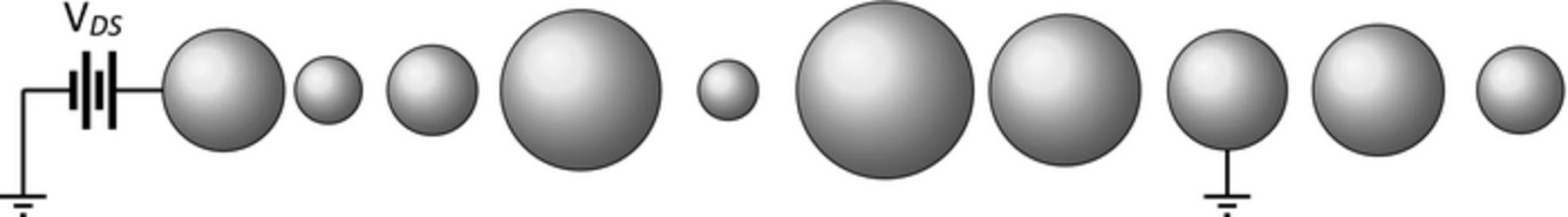
Figure 1. Schematic of the geometrical model of a 1D chain of gold nano-islands deposited on an insulating wire used for investigating the physical mechanisms. The island radii and junction widths are randomly selected over uniform distributions to model the position of metallic islands in an experimental device fabricated by Lee et al.4
We have examined at T = 0 K the up-steps for the disordered 25-junction chain system previously studied by Savaikar et al.,16 which has reasonably strong inter-island couplings, and for which the inter-island spacings vary over a range from ∼1.1 nm to ∼4.9 nm and island radii vary from ∼4.2 nm to ∼9.6 nm. The model device is schematically shown in Fig. 1. The simulation methods are the same as described by Savaikar et al.16 A total of 32 up-steps were observed while increasing VDS in increments of ∼74 × 10−9 V from zero up to Vth = 0.74 V. Figure 2 shows the static charge distribution in the 25-junction system as it evolves with increasing VDS > 0 after overcoming each particular up-step. It is observed that upon overcoming an up-step the new static charge state may not necessarily advance the charge front toward the source. For example, as the system overcomes the up-steps from 6 to 10, the charge front does not advance but remains at the twelfth island. Furthermore, overcoming of an up-step and propagation of the charge front need not necessarily involve a change in the net charge on the device as observed during the overcoming of the last up-step, although overcoming all the remaining up-steps in the system is accompanied by a change in net charge on the device (see Fig. 2 and Table I). For a positive VDS, the net charge on the device in any static charge state is positive, with each charged island carrying a net positive. On the other hand, for a negative VDS at T = 0 K, we have observed that the net charge on the device is negative with each charged island carrying a net negative charge. At T = 0 K for a positive VDS, it is highly unlikely that any island would carry a net negative charge when the system is in a static charge state. It is observed that after up-step number 32 is overcome, the system has reached its Vth with the arrival of the charge front to the source, and a small steady-state current begins to flow.
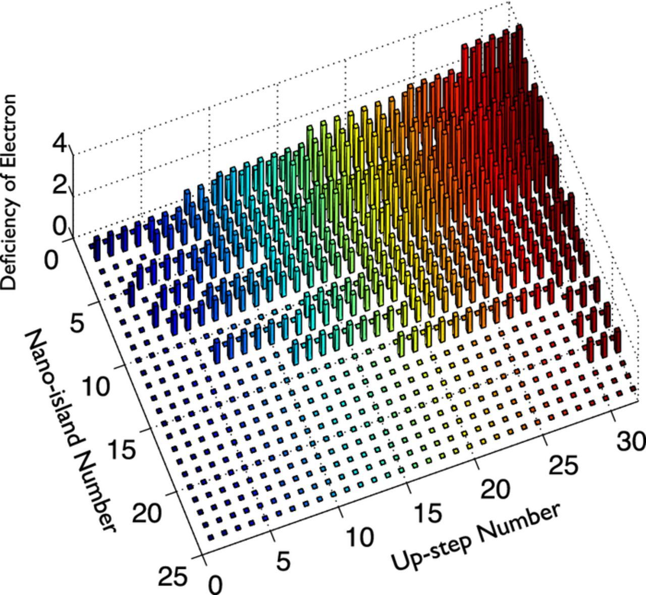
Figure 2. The static charge distribution in the 25-junction system at T = 0 K as the system evolves with increasing VDS in increments of ∼74 × 10−9 V after overcoming each particular up-step of the total 32 up-steps. The vertical axis shows the excess electron number (in this case, a deficiency of electrons) on each island at a particular VDS. The rows numbering from 1 to 24 along one of the horizontal axes represent the 24 islands in the sequential order from the drain to the source. The other horizontal axis indicates the sequential up-step number from 1 to 32. Overcoming of an up-step need not necessarily be accompanied by the propagation of charge front (for example, up-steps from 11 to 17), nor it be accompanied by an increase in the net charge on the device as observed in the overcoming of the last up-step.
Table I. The net charge (total number of electrons) present on the two electrodes at each up-step. The magnitude of sum of the net charges on the two electrodes at any particular up-step is equal to the magnitude of net charge that is present on the device at that particular up-step.
| Up-step | 1 | 2 | 3 | 4 | 5 | 6 | 7 | 8 | 9 | 10 | 11 | 12 | 13 | 14 | 15 | 16 | 17 | 18 | 19 | 20 | 21 | 22 | 23 | 24 | 25 | 26 | 27 | 28 | 29 | 30 | 31 | 32 |
| Drain | 1 | 2 | 3 | 4 | 5 | 6 | 7 | 8 | 9 | 10 | 11 | 12 | 13 | 14 | 15 | 16 | 17 | 19 | 20 | 21 | 22 | 23 | 24 | 25 | 26 | 27 | 28 | 29 | 30 | 33 | 34 | 834 |
| Source | 0 | 0 | 0 | 0 | 0 | 0 | 0 | 0 | 0 | 0 | 0 | 0 | 0 | 0 | 0 | 0 | 0 | 0 | 0 | 0 | 0 | 0 | 0 | 0 | 0 | 0 | 0 | 0 | 0 | 0 | 0 | −800 |
The first electron moved across the first junction from the first island to the drain at VDS = 8.78 × 10⁻² V thereby overcoming the first up-step. The first junction is, however, not the junction with the minimum Ec, as can be seen from the Ec distribution in Fig. 3 for the 25-junction chain device. The values of ΔV required to overcome each subsequent up-step ranged anywhere from ∼7.4 × 10⁻⁸ V up to 1.54 × 10⁻¹ V (Fig. 4). In the process of overcoming an up-step, frequently one electron and sometimes two to three electrons (e.g. up-step numbers 18 and 30 in Fig. 2 and Table I) were observed to move to the drain, leading to a change in the net positive charge on the device during the overcoming of an up-step. The flow of more than a single electron to the drain suggests that there might actually exist additional up-steps that require less than the incremental value of 74 × 10−9 V for them to be overcome. During the course of overcoming the 32 up-steps, the charge front advanced only nine times toward the source (Fig. 2). Although it is difficult to establish the relation between the number of up-steps, the size of the up-steps ΔV, and Ec, it is observed that a large number of the up-steps (24 out of the 32) arise when the advancing charge front is halted by junctions with large Ec (junctions 13, 15 and 17), especially by those that are further away from the biased drain (junction 17, see Fig. 2). It is to be noted that these junctions are not necessarily the junctions having the maximum Ec (junction 18 has the maximum Ec, see Fig. 3). Overall, however, we observe that a large fraction of the Vth is required to overcome the up-steps when the charge front is halted by large Ec junctions. For example, ∼62% of Vth is utilized to push the charge front across junctions 13 and 17. Overcoming of these "large" up-steps is also accompanied by a considerable increase in the net charge on the device, which helps the electrons to tunnel through large Ec junctions by developing sufficiently large potential drops across these junctions. For example, when the charge front is stuck on island 16 halted by junction 17, the net charge on the device increased by +11e (from +19e to +30e in up-steps 18–29, see Fig. 2 and Table I). When it finally advances past island 16, the net charge on the system changes from +30e to +33e. After overcoming all the up-steps at the Vth, the system attains a characteristic "long lived" background charge state and starts conducting.
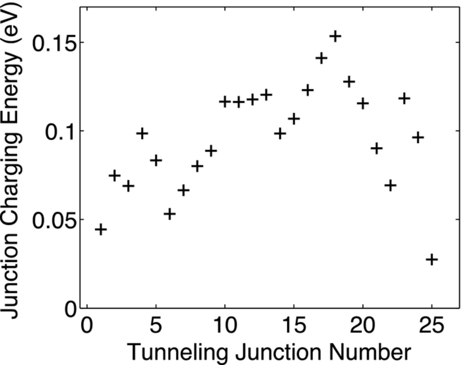
Figure 3. Distribution of charging energies in a 25-junction chain device having random distribution in junction widths (∼1.1 nm to ∼4.9 nm) and island radii (∼4.2 nm to ∼9.6 nm), and reasonably strong inter-island couplings and self-capacitances.
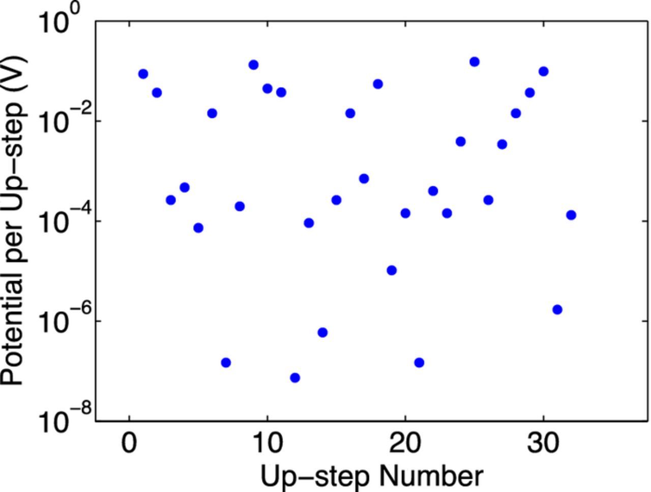
Figure 4. ΔVrequired to overcome each up-step at T = 0 K in the 25-junction chain device before the device reaches the Vth = 0.74 V and begins to conduct. Due to the system disorder, strong inter-island coupling, and larger λ, ΔV is widely distributed ranging anywhere from ∼74 × 10−9 V up to 154 × 10−3 V making it difficult to predict from the native device structure what the up-steps will be, and therefore, what the Vth will be, unlike in an uncoupled uniform system.14
Similar observations in a 12-junction chain device demonstrate that the device begins to conduct after overcoming 6 up-steps with ΔV values that spread over a wide range from 140 × 10−6 V to 88 × 10−3 V. From these observations it appears that it is difficult to analytically predict the number of up-steps for a given chain length in which the islands are strongly coupled to one another. Unlike in the uniform system studied by Middleton and Wingreen,14 in a disordered system with stronger inter-island coupling, the larger-λ limit leads to potential drops across the junctions that change as the charge states change. The change in potential drops along with the distribution of Ec make it difficult to predict from the native structure what the up-steps will be, and therefore, ultimately what the Vth will be. The set of ΔV values required to overcome the up-steps varies over a wide range that only increases with increasing chain length. Furthermore, it is difficult to identify the specific junction across which the system expends maximum energy to drive ahead the charge front when the charge front stops advancing. Because of the variable voltage drops across the junctions as the charge front advances, that junction need not be the one with the maximum Ec, although the results of this analysis indicate that it is typically from among those that have larger Ec values, which are largely those associated with smaller islands.16
Physical Mechanism Leading to the Coulomb Staircase Structure
When the device reaches the Vth at T = 0 K, the charge front reaches the grounded source electrode and the device starts conducting. Savaikar et al.16 showed that 1D chains with sufficient structural disorder exhibit interesting staircase structures in their IV characteristics at low VDS, especially at lower T, and which are more pronounced for longer chains. We are unaware of any previous work that has clearly and comprehensively explained the detailed mechanism behind the origin of CS structures, especially in multi-island SEDs with inter-island couplings. In this section, we describe the microscopic details of the mechanism behind the current flow in multi-island one-dimensional SEDs at low VDS that leads to CS structures as the VDS increases.
When a one-dimensional multi-island SED enters the conducting state at VDS = Vth after having overcome all the up-steps, it attains a unique longest-lived charge distribution for the given VDS that we refer to as the device's longest lifetime state (LLS). The LLS of the system is the state in which the system spends the longest amount of time (waiting time) before the rate-limiting step (RLS) transition takes place. The RLS transition is the slowest electronic transition that occurs across a particular tunneling junction in a given device for a given VDS during which the system exits the LLS. The RLS transition is followed by a series of fast transitions (cascade) that leads to a net flow of charge across the device giving a non-zero current, and ends with the system back again in the LLS. The cascade of transitions may not necessarily occur in the sequential order of the junctions. At any particular VDS, the microscopic observation of the charge states of the system during its temporal evolution shows that the waiting time for the RLS transition predominantly determines the device current at that particular bias. Therefore, the junction across which the RLS transition occurs acts as the current-limiting junction (CLJ). At T = 0 K, and moderate source-drain bias (in the range in which CS structures are evident in the IV characteristic) the number of MC steps required for the system to return back to its LLS is observed to be an integral multiple of the number of junctions in the system. During the time the system returns back to the LLS, net one electron is transferred across the device from the source to the drain. Along a CS step, as VDS is increased, the LLS stays the same, and the RLS transition rate increases only slightly due to the increased bias, until the next step appears in the staircase structure. The transition rates of the subsequent fast transitions across the other junctions following the RLS transition may drastically vary as the system periodically (in terms of MC steps) returns back to the LLS. However, these fast-rate transitions do not have any major impact on the steady-state ISD. Therefore the device current (ISD) shows only a small increase until VDS reaches the second step where there is a change in the background charge distribution leading to a change in the LLS and associated RLS, where a different junction acts as the CLJ. Typically, it is observed that the new background charge state and an increase in VDS result in a new CLJ with an increased transition rate. Therefore the device exhibits a relatively sharp increase in the current leading to a step-like structure in the IV curve. Since the increase in device current between the two consecutive staircase steps is typically very small as compared to the change in current at a step, the IV curve appears practically flat between any two consecutive thresholds in the IV characteristics. At each successive CS threshold, the charge distribution in the LLS of the system may change considerably, especially as VDS gets larger. The change in the background charge distribution may open up new conduction channels in the bias-charge-state space.16 Most frequently when the current transitions from one step to the next, the net charge on a few of the islands that are already charged increases by one unit and some of the uncharged islands are likely to become charged. With the new charge distribution that is accompanied by a change in LLS, RLS, and a change in CLJ, the device carries a larger current at each successive threshold. This process continues with the increasing bias at low VDS values giving rise to a CS structure in the device IV characteristics. As VDS increases more conduction channels16 open up in the bias-charge-state space, each with its own comparable LLS. Each of the several LLS having comparable lifetimes may contribute significantly in determining the overall device current, especially at larger VDS. Furthermore, the number of possible transitions and their transition probabilities at any given point of time increase with increasing VDS and the dominance of any one LLS subsequently diminishes. Hence the periodicity in the evolution of charge states breaks down, and the step structure washes out at sufficiently high VDS.
In order to illustrate the mechanism described above, we have investigated the evolving charge microstates at T = 0 K as a function of increasing VDS in a 12-junction chain device. The device consists of islands whose sizes vary over a range from ∼4.5 nm to ∼9.6 nm and whose spacings vary from ∼1.4 nm to ∼4.9 nm. The IV characteristics showing discrete coulomb staircase steps are presented in Fig. 5. When the device switches on at Vth = 0.14 V, the system has a LLS charge distribution that is shown in Fig. 6. It can be seen that at VDS = 0.14 V five of the eleven islands are charged, each one carrying a net positive charge of +e (electron vacancy), while the remaining islands are still neutral. At VDS = 0.14 V, the RLS transition occurs at the rate of 6.5 × 10⁷s− 1 (Fig. 7) across the first junction, coupling the first island to the drain, thereby yielding a device current of 7.9 × 10− 12A. Therefore the first junction acts as a CLJ at Vth = 0.14 V. The RLS transition across the first junction is followed by a cascade of transitions across the remaining junctions in a non-sequential order, with their rates ranging anywhere from 6.8 × 10⁸ s−1 to 5.2 × 10¹³ s−1 (Fig. 7), as the system periodically (in terms of MC steps) returns back to its LLS while VDS is fixed at 0.14 V. It is observed that the system most frequently returns back to the LLS after 12 steps (inset in Fig. 7), which is the number of junctions present in the system. The inset shows a close-up view of the rate at which the system exits the LLS with a specific charge distribution, and the rates of the subsequent transitions with different charge distributions before the system finally returns back to the LLS again. During this time period, net one electron flows across the device from the source to the drain. Since the rates are very sensitive to the charge state of the system, it is apparent from the transition rates in Fig. 7 that the system nearly periodically visits the same charge state every time it returns back to its LLS as it evolves through the cycle of MC steps. This has been observed in the simulation data. As the system evolves, sometimes rare events having smaller probabilities and shorter lifetimes occur in the system (see, for example, near Monte Carlo step 300 in Fig. 7). However, it is observed that the system, through self-correcting transitions, returns back to the expected LLS, but taking a larger number of steps, which is a higher multiple of 12. The periodic process repeats yielding a flow of charge across the device, unless there is a sufficient change in VDS. When VDS is increased to 0.16 V, the net charge in the system increases by +e (Fig. 6) from +5e to +6e and a rearrangement of the charge takes place in the LLS of the system. Due to the rearrangement of the charge and the small increase inVDS, it is observed that the transition rate across the first junction, which earlier predominantly influenced the ISD, increases substantially from 6.5 × 10⁷ s−1 to 1.9 × 10¹⁰ s−1. Importantly, the first junction does not determine the device current anymore. Rather, the RLS transition now occurs across the ninth junction making it the CLJ. At VDS = 0.16 V, the new CLJ transfers an electron at the rate of 6.9 × 10⁸ s−1, thereby limiting the device current to 50.4 × 10− 12 A. When VDS is increased from 0.14 V to 0.16 V, the rate of the RLS transition jumps by a factor of ∼10 and the device current increases by a factor of ∼6 (inset in Fig. 5). As the bias is further increased beyond VDS = 0.16 V, no appreciable change takes place in ISD up to VDS = 0.34 V. Despite the change in the LLS caused by an increase in the net charge on the device at VDS = 0.34 V (see Fig. 6), the increase in the current is observed to be negligible (on the scale shown) caused by the only small increase in the rate of the RLS transition that continues to occur across the ninth junction and limit the device current, thus giving rise to the first CS step in the IV characteristic. When VDS further increases to 0.38 V, the RLS transition now occurs across the tenth junction with a higher transition rate thereby sharply increasing the device current further, and giving rise to the second step of the CS in the IV characteristic. At VDS = 0.38V, the net charge in the device in its LLS increases to +13e. The net charge on few of the already charged islands increased by one unit charge (+e) and few of the neutral islands became charged. The three junctions 1, 9, and 10 that act as CLJs at three different VDS values of 0.14, 0.16, and 0.38 V are among the wider junctions along the chain. As the bias is increased further, the same process continues with every change in the CLJ most frequently giving rise to a sharp step in the IV that is accompanied by an increase in the net charge in the device, a change in the LLS, and an increase in RLS transition rate. The multiple possibilities of transitions along with their higher transition probabilities at larger VDS, and the increasing similarities of lifetimes of LLS of different conduction channels in the bias-charge-state space ultimately lead to diminishing of the staircase steps in the IV characteristics at larger VDS. Similar observations were made in devices of different chain lengths such as the 25-junction system discussed earlier.
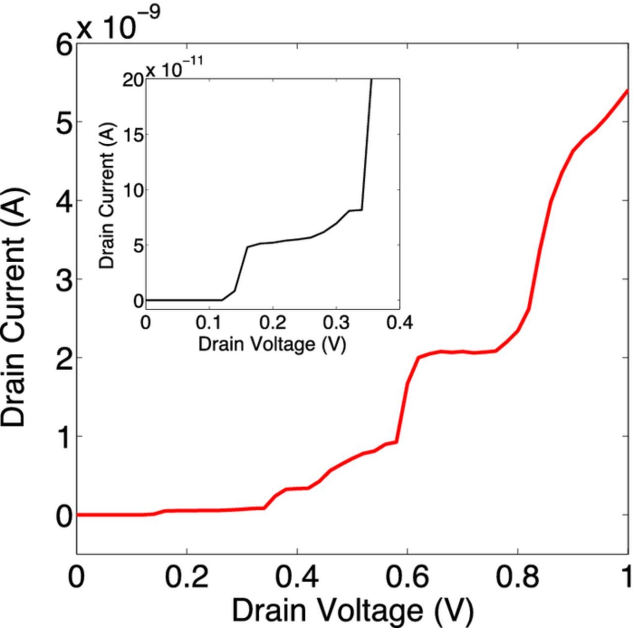
Figure 5. The IV characteristics of the 12-junction chain device at T = 0 K. After the device begins to conduct at Vth = 0.14V, it exhibits discrete, non-uniform staircase-step like structures that are characteristic of the disorder in the chain. The device shows a sharp increase in ISD at every threshold due to the change in the current-limiting junction (CLJ) accompanied by a change in the longest lifetime state (LLS) and an increase in the rate-limiting step (RLS) transition rate. In between any two consecutive thresholds, ISD shows a negligible increase (on the scale) with the increasing VDS due to the negligible increase in the RLS transition rate across a particular junction that makes the IV curve appear practically flat along the step. The inset shows the close-up view of the IV characteristics.
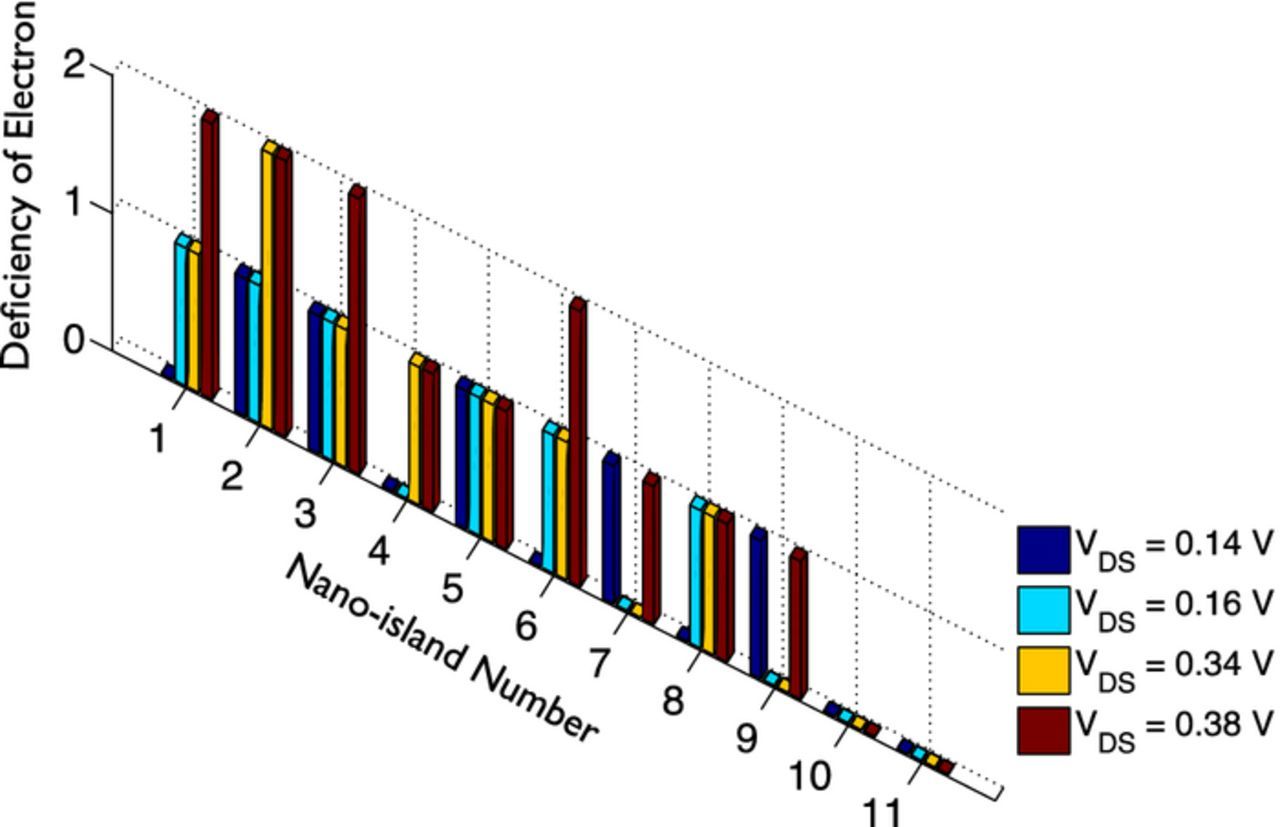
Figure 6. The net charge distribution on each island in the 12-junction chain device at T = 0 K in its LLS at three different threshold values of VDS = 0.14, 0.16, and 0.38 V. The horizontal axis represents the 11 nano-islands in the sequential order from the drain to the source while the vertical axis shows the excess electron number (in this case, a deficiency of electrons) on each island. At every subsequent threshold the net charge on the device increases, not necessarily accompanied by an increase in charge on all the islands, that typically leads to a change in current-limiting junction (CLJ), change in the longest-lifetime state (LLS), and an increase in rate-limiting step (RLS) transition rate, ultimately leading to a sharp increase in ISD.
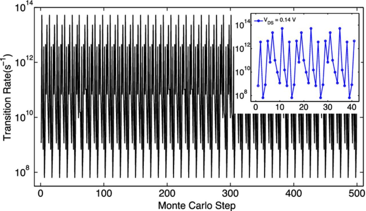
Figure 7. The total transition rate in the device at T = 0 K and VDS = 0.14 V when the device just begins to conduct. Because of the large disorder in the device especially in junction widths, only one junction is energetically favorable for transition at any particular time (Monte Carlo step), and the transition rate varies over a considerably large range anywhere from 6.5 × 10⁷ s−1 to 5.2 × 10¹³s−1. The RLS transition rate (6.5 × 10⁷ s−1) across a particular junction determines the overall device current. The inset (close-up view) shows the periodicity (12 steps for the 12 junction system) in the evolution of the system charge states as the steady-state system returns back to its LLS during which a net charge flows across the device from the source (right in Fig. 1) to the drain (left in Fig. 1) giving a non-zero average current.
On a concluding note, the disorder in a capacitively coupled 1D chain is primarily responsible for the CB and CS structures in the device IV characteristics. The large Ec junctions that tend to couple the smaller islands act as major barriers to the charge propagation as the device approaches its Vth, thereby predominantly contributing to the coulomb blockade and the Vth. When the device begins to conduct, the wider junctions that most frequently act as CLJs predominantly determine the device current. For a given device, it is difficult to predict the CB and the nature of the CS from its native structure. This study inspires further investigations on experimentally fabricated one- and multi-dimensional devices. For example, a disordered 1D device is expected to exhibit different CS structures, and possibly different Vth values when the electrodes are exchanged under the same bias conditions. Multi-dimensional device structures are less likely to exhibit CS structures in their IV characteristics even at lower temperatures.5,6,17,18 This is because such structures are either likely to have conduction spread out over many possible conduction paths, or, they would behave like quasi-1D devices having a dominant conducting path depending on the disorder in the system. If conduction is spread over many possible conducting paths, the average IV behavior over all paths would "wash out" the CS structure of any one path. On the other hand, in cases of sufficient disorder where there would be one or a few dominant conducting paths, those dominant paths would likely be made of a subset of relatively narrower junctions17,18 and larger islands from among the respective distributions in the whole device. The distributions sampled in the dominant conducting paths would exhibit less pronounced CS structures due to the higher degree of uniformity in their island sizes and junction widths. We further expect that in the simulations carried out at non-zero temperature, the device behavior may reveal a thermally activated nature of the Coulombic barriers in 1D structures and also the opening of new conduction paths in multi-dimensional structures with the increasing temperatures. All these studies require a systematic experimental investigation that may potentially validate the proposed mechanisms.
Acknowledgments
We are grateful to Douglas Banyai and Y. K. Yap for stimulating discussions. Simulations were conducted using the MITS simulation software.16 Results presented here were obtained in part using the high performance computing cluster wigner.research.mtu.edu in Information Technology Services and rama.phy.mtu.edu in the Physics Department at Michigan Technological University.
M.A.S. designed the numerical experiments and carried out the simulations primarily under the guidance of J. A. J., and was the primary author of the manuscript. All three authors defined the scope of the work and the direction of the effort. M.A.S. and J.A.J. analyzed the data. All three authors discussed the results and contributed to writing the manuscript.