
Abstract
Uniformly arrayed single- and multi-directional slanted Cu nanorods on a Si substrate were fabricated using a template of slanted channel structures. The single-directional slanted Cu nanorods were obtained using slanted channel structures oriented at an angle of 15° with respect to the surface normal. Double- and quadruple-directional slanted Cu nanorods were obtained using double- and quadruple-directional slanted channel structures, respectively. The double-directional Cu nanorods were symmetrically slanted at 30°, preserving the architecture of the slanted channel structures. The quadruple-directional slanted Cu nanorods had pyramidal structures, with slanted rods positioned at 30° from the surface normal to the right, left, front, and back.

This is an open access article distributed under the terms of the Creative Commons Attribution Non-Commercial No Derivatives 4.0 License (CC BY-NC-ND, http://creativecommons.org/licenses/by-nc-nd/4.0/), which permits non-commercial reuse, distribution, and reproduction in any medium, provided the original work is not changed in any way and is properly cited. For permission for commercial reuse, please email: oa@electrochem.org.
One-dimensional metal nanostructures have attracted much attention because of the unique properties of nanoscale materials compared to those of the bulk.1 In particular, one-dimensional Cu nanostructures such as nanorods or nanopillars have been applied to battery electrodes,2,3 micro-sized heating pipes,4 boiling or cooling devices,5,6 and photocatalysts.7
Template-based electrochemical deposition is generally employed for the growth of Cu nanorods. Anodic aluminum oxide (AAO) templates have been widely used for fabricating Cu nanorods because the material typically possesses a relatively uniform pore distribution.2,3,8,9,10 With the templating method, the diameter and periodicity of the Cu nanorods can be precisely controlled by adjusting the characteristics of pores in the templates. The method is relatively simple and inexpensive; however, the angles of the Cu nanorods are limited by the use of vertical structures, which are perpendicular to the substrate surface.
Slanted Cu nanorods have been used in heat-transfer devices,5,6 and have potential applications in the above-mentioned fields. Oblique angle deposition has been used exclusively for the fabrication of slanted Cu nanorods.5,11,12 The oblique angle deposition technique is based on deposition at oblique anlges, where the trajectories of the incident vapor fluxes are directed off-normal (oblique) to the substrate.13–15 Self-shadowing occurs in the initial nucleation stage, preventing film growth in these regions. The resulting film is inclined in the direction of the vapor source. By rotating the substrate properly, the angle and shape of the structures can be controlled. In oblique angle deposition, the control of the process parameters is relatively simple and various metallic sources can be used. However, extremely precise control over the surface angle is required and the deposited films are usually porous. Controlling the periodicity of the columnar structures in a large area is also difficult, because the columns easily aggregate with each other during deposition.6,11 Şeşen et al. reported that slanted Cu nanorods fabricated by oblique angle deposition were disadvantageous for heat-transfer devices because the denser Cu nanorods, which formed film-like rod structures, acted as thermal resistors.6 Therefore, it is important to control the periodicity and angle of slanted Cu nanorods for use in the above-mentioned applications.
Recently, a slanted plasma etching technique for the fabrication of single- and multi-directional slanted channel structures was reported.16 Because slanted plasma etching can be performed under practical plasma processing conditions, it is advantageous for fabricating slanted patterns over a large area with excellent uniformity in pattern height and diameter. The method also precisely controls the angle of the slanted patterns by the use of a specially designed Faraday cage system, which allows one to control the angle of ions incident on the substrate. Therefore, slanted channel structures prepared by slanted plasma etching may be adequate as templates for the fabrication of uniform arrays of slanted Cu nanorods.
In this study, single- and multi-directional slanted Cu nanorods on a Si substrate were fabricated using slanted channel structures as templates. The single-, double-, and quadruple-directional slanted channel structures were obtained by slanted plasma etching of Si under practical plasma processing conditions.
Figure 1 shows a schematic of the fabrication of single- and multi-directional slanted Cu nanorods. Single- and multi-directional slanted etch profiles (channel structures) of Si were prepared by slanted plasma etching. The slanted plasma etching process was conducted using a Faraday cage system, which was described in detail in a previous study.16 The material used to create the channel structures was a Si substrate with a polycrystalline Si (poly-Si) film on the etch stop layer. A pattern of holes was delineated on the poly-Si film by optical lithography. SiO2 was used as both a mask and an etch stop layer. Poly-Si was grown by low pressure chemical vapor deposition (LPCVD) with silane. SiO2 was deposited by plasma-assisted chemical vapor deposition (PECVD) with tetraethoxysilane (TEOS). The thicknesses of the poly-Si film and SiO2 mask were 1100 nm and 372 nm, respectively. The widths of the mask and open spaces were 390 nm and 417 nm, respectively.
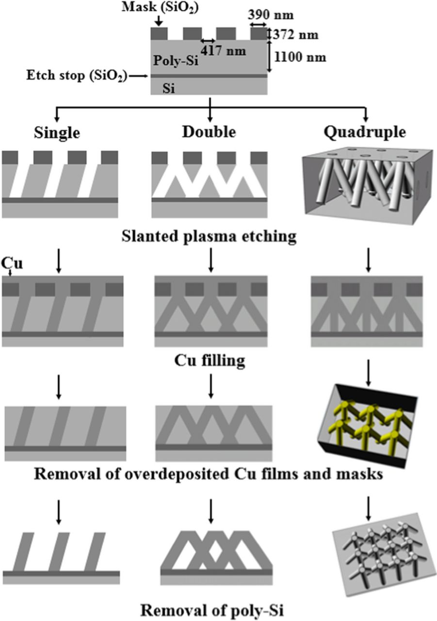
Figure 1. Schematic of the fabrication of single-, double-, and quadruple-directional slanted Cu nanorods.
The slanted channel structures within the Si were filled with Cu by electroless plating. The substrate was activated in 1 L of an aqueous solution containing 0.1 g PdCl2, 5 mL 50% HF, and 3 mL 35% HCl for 40 s. Electroless plating of Cu was then carried out in 1 L of an aqueous solution consisting of 5 mL 2, 2′-dipyridyl, 5 g CuSO4·5H2O, 15 g ethylenediaminetetraacetic acid (EDTA), and 5 mL paraformaldehyde (HCHO)n. The plating was performed at a constant temperature of 85°C for 420 s. The pH of the plating solution was adjusted to approximately 12.5 using a 0.5 M KOH solution. The conditions for the electroless plating of Cu employed in this work were similar to those used for the interconnection of Cu in ultra large scale integrated (ULSI) circuits.17
When electroless plating of Cu was conducted to fill the slanted channel structures, Cu was overdeposited in order to ensure the complete filling of the channel structures. The films of overdeposited Cu and the SiO2 masks were removed using chemical mechanical polishing (CMP). CMP was performed using polishing equipment (M-Prep 3, Allied High Tech) at a rotational speed of 40 rpm. Alumina slurry (0.8 μm in size) was used as an abrasive.
Finally, wet etching was performed to remove the remaining poly-Si of the channel structures between the Cu rods. Wet etching was conducted in 1 L of an aqueous solution containing 100 g KOH and 200 mL normal propanol (n-propanol) maintained at a temperature of 85°C. This solution is commonly used to remove Si in the fabrication of ULSI circuits.18
Single-directional slanted Cu nanorods were successfully obtained using the single-directional slanted Si channel structures as a template. The angle of the slanted Si channel, which was defined with respect to the surface normal, could be controlled by varying the angle of the sample holder in the Faraday cage.16 In this study, the angle of the single-directional slanted channels was 15°. Figure 2 shows a scanning electron microscopy (SEM) image of the single-directional slanted Cu nanorods after the removal of poly-Si. It is clearly seen that the single-directional slanted Cu nanorods are uniformly arrayed at an angle of 15° on the Si substrate. The diameter and length of the slanted Cu nanorods were 360 and 1006 nm, respectively. Note that the diameter and length of the Cu nanorods can be controlled by varying the dimensions of the slanted Si channel structures, which in turn can be controlled by changing the process conditions for slanted plasma etching. Based on our previous results,19,20 it is expected that slanted Cu nanorods having diameters less than 100 nm and angles as high as 60° can be obtained.
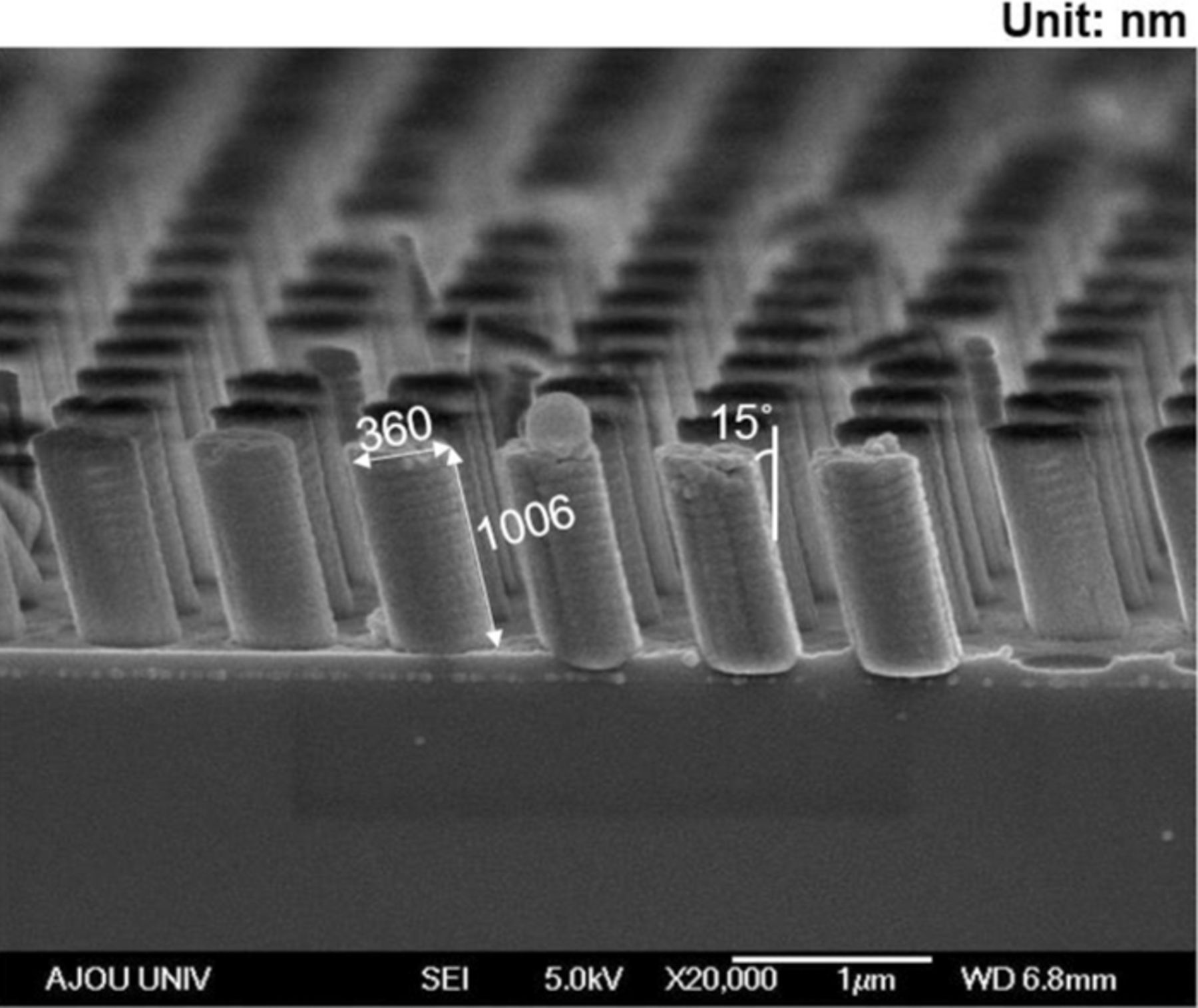
Figure 2. SEM image of the single-directional slanted Cu nanorods using single-directional slanted Si channel structures as templates.
The microstructural properties of the single-directional slanted Cu nanorods were characterized using X-ray diffractometer (XRD). The XRD spectrum (not shown here) of the slanted Cu nanorods showed two distinct peaks corresponding to Cu (111) and Cu (200) planes, respectively. Therefore, the single-directional slanted Cu nanorods obtained in this study are polycrystalline with preferred orientations of (111) and (200) planes. This agrees with other studies on electroless plating of Cu using CuSO4·5H2O as a Cu precursor.21
Because the uniform array of single-directional slanted Cu nanorods was successfully fabricated using corresponding channel structures as a template, it is expected that multi-directional, such as double and quadruple, slanted Cu nanorods could be obtained if corresponding double- and quadruple-channel structures, respectively, are provided. Figure 3 shows the SEM image of the double-directional slanted Cu nanorods based on double-directional Si channel structures having angles of 30° with respect to the surface normal. The double-directional slanted Cu nanorods have uniform and symmetrical structures positioned at angles of 30° to the surface normal in opposite directions. The diameters of the slanted Cu nanorods in each direction are nearly equal to 300 nm, which also indicates the good symmetry of the array.
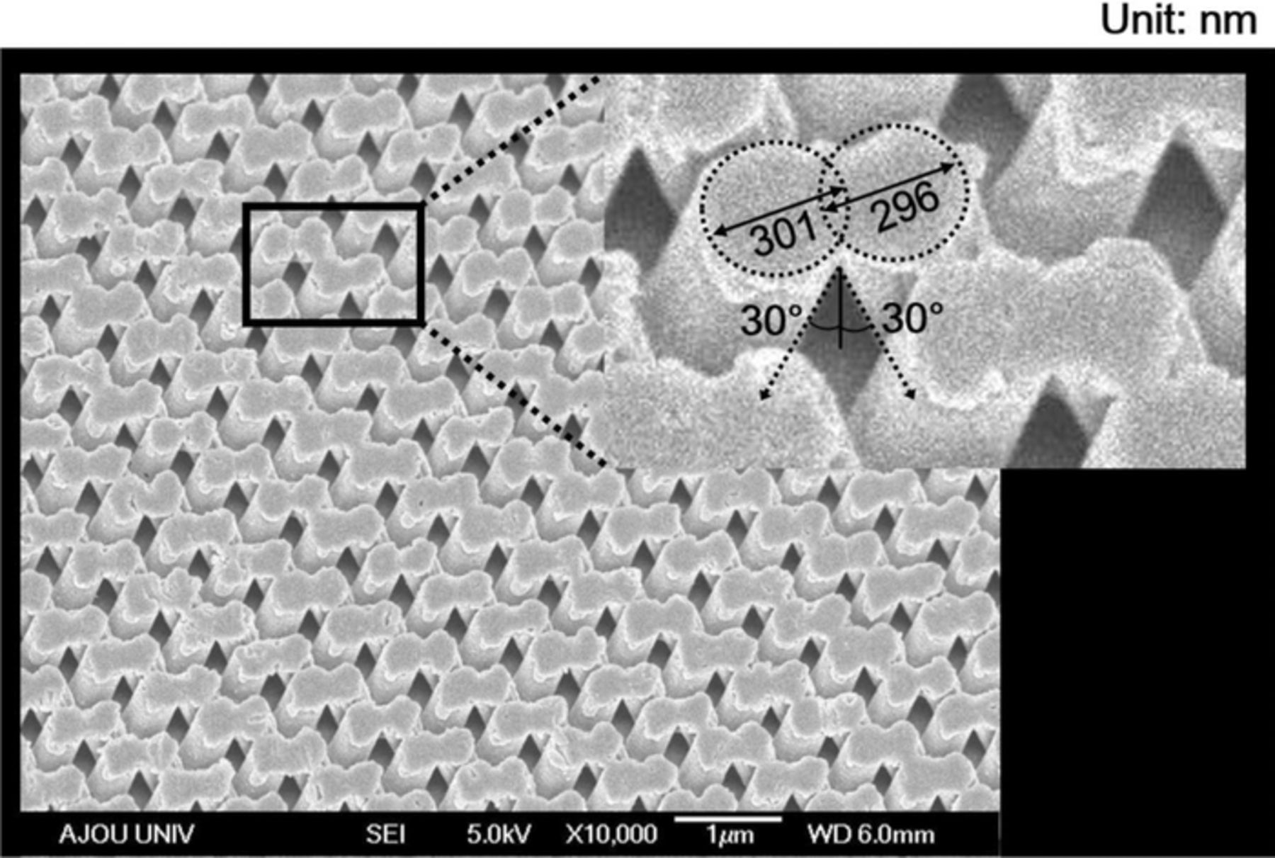
Figure 3. SEM image of the double-directional slanted Cu nanorods using the double-directional slanted Si channel structures as templates.
Quadruple-directional slanted Cu nanorods were obtained using quadruple-directional Si channel structures. The quadruple-directional Si channel structures were symmetrical with angles of 30° to the surface normal in four directions. Figure 4 shows SEM images with top and cross-sectional views of the quadruple-directional slanted Cu nanorods. A three-dimensional model of the quadruple-directional slanted Cu nanorods is also shown for the sake of visualization. The quadruple-directional slanted Cu nanorods viewed from the top show patterns similar to plaid because they have a pyramidal structure. In Figure 4a, the bright part represents Cu while the dark part represents the open spaces. The diameters of the slanted Cu nanorods in the right/left and forward/backward directions were 479 and 411 nm, respectively. The sample was cut in the direction of the “cleaving line” indicated on Figure 4a. As shown in this cross-sectional view in Figure 4b, the slanted Cu nanorods have angles of 30° with respect to the surface normal. This implies the successful fabrication of the quadruple-directional slanted Cu nanorods in uniform arrays.
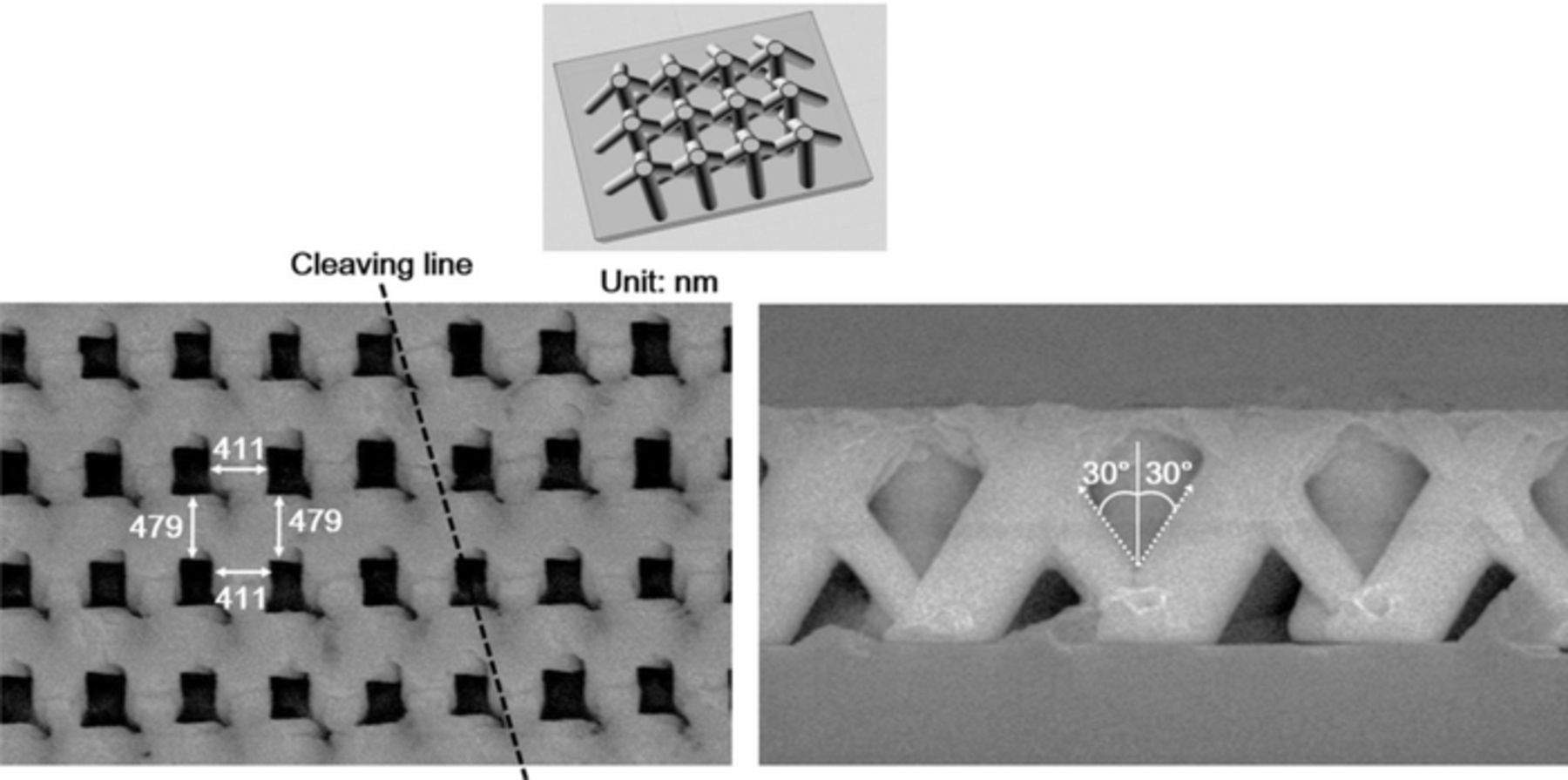
Figure 4. SEM images showing (a) top and (b) cross-sectional views of the quadruple-directional slanted Cu nanorods using quadruple-directional slanted Si channel structures as templates. The three-dimensional model of the Cu nanorods at the top schematically indicates the contents of the two micrographs.
As mentioned earlier, Cu nanostructures such as nanorods or nanopillars find applications in battery electrodes, boiling or cooling devices, and so on. The use of multi-directional structures have advantages in these applications because the multi-directional structures increase the specific surface area of the substrate, improving the performance of the devices. For example, the specific areas of the substrate having double- and quadruple-directional Cu nanorods prepared in this study are increased to around 1.5 and 4.3 times, respectively, compared to that having single-directional Cu nanorods.
In summary, uniform arrays of single- and multi-directional slanted Cu nanorods were realized using plasma-etched slanted channel structures as templates. The single-, double-, and quadruple-directional slanted channel structures of Si were obtained by a slanted plasma etching technique. The angles, diameters, and lengths of the single- and multi-directional slanted Cu nanorods showed excellent uniformity and symmetry, demonstrating the successful transfer of the template architecture from the corresponding slanted channel structures. This work offers a novel method for the fabrication of uniformly arrayed slanted metal nanostructures with controllable sizes and angles.
Acknowledgments
This work was supported by the National Research Foundation of Korea (NRF) grant (grant Nos. 2012R1A2A2A01004416 and 2015R1A2A2A01002305).