
Abstract
Room temperature ferroelectricity in pulsed laser deposited rare-earth doped hafnium oxide (HfO2) thin films is discussed. Maximum values of remnant polarizations (Pr) ∼13.5 and 12 μC/cm2 along with coercive fields (EC) ∼334 and 384 kV/cm are observed in 6 mol. % of rare-earth (Sm or Gd) doped-HfO2 thin films (Sm:HfO2 and Gd:HfO2), respectively. Piezoresponse force microscopy measurements confirmed ferroelectric nature of films by showing phase hysteresis and butterfly amplitude loops. It is noticed that wake-up cycles improved the remnant polarization and found to be necessary for the forming of well saturated hysteresis loops. Our results showed potential toward realization of future highly scaled non-volatile ferroelectric memories.

This is an open access article distributed under the terms of the Creative Commons Attribution 4.0 License (CC BY, http://creativecommons.org/licenses/by/4.0/), which permits unrestricted reuse of the work in any medium, provided the original work is properly cited.
Ferroelectric materials are engendering considerable interest because of a variety of emerging applications including ferroelectric memories which have promising potentials for next generation high integration density and low power nonvolatile memory technology.1,2 The most studied material for ferroelectric memories, Pb[ZrxTi1-x]O3 (PZT),1 is facing severe scaling limitations due to its complicated crystal structure which in turn hinders its applicability toward dense integration in the complementary metal oxide semiconductor (CMOS) technology. The lead (Pb) toxicity in PZT is also a snag due to ecological concerns.
Recently, experimental as well as theoretical studies showed ferroelectricity in doped hafnia (HfO2) thin films which are compatible with existing CMOS technology.3–10 Ferroelectric phenomenon in these doped-HfO2 films deposited by various deposition techniques such as atomic layer deposition,5–10 chemical solution deposition,11 and sputtering12 was mainly explained by the existence of noncentrosymmetric orthorhombic phase (space group of Pca21).5,6,12 The dopant incorporation into monoclinic HfO2 matrix results in a transformation to tetragonal/cubic phase with the appearance of an intermediate metastable orthorhombic (Pca21) phase. On the other hand, in some of the reports, ferroelectric nature in doped-HfO2 films was attributed to the influence of “wake-up” effect.11–13
In this paper, we report on the ferroelectric properties of rare earth doped Sm:HfO2 (SHO) and Gd:HfO2 (GHO) thin films fabricated by the sequential pulsed laser deposition (SPLD) technique.14–16 The deposition was performed by periodic depositions from HfO2 and Sm2O3/Gd2O3 ceramic targets. The dopant concentration was obtained by controlling number of Sm2O3/Gd2O3 ablation pulses relative to that of HfO2. To study the ferroelectric properties of the deposited samples, polarization-voltage (P-V), capacitance-voltage (C-V), and piezoresponse force microscopy (PFM) measurements were performed.
Experimental
Polycrystalline thin films of SHO and GHO of ∼60 nm thickness were fabricated on Pt/TiO2/SiO2/Si substrates by SPLD technique at a fixed temperature of 650°C and in an oxygen ambient partial pressure of ∼0.5 Pa. The KrF excimer laser (248 nm, 10 Hz) operating at an energy density of ∼2.1 J cm−2 was used for the ablation of the Sm2O3 (SO), Gd2O3 (GO) and HfO2 (HO) ceramic targets, synthesized by solid state reaction method. With this set of parameters, the deposition rate was determined to be about 0.01 nm/pulse for all three oxide materials. During the sequential ablation of ceramic targets, concentration of Sm/Gd dopant in HfO2 matrix was controlled by varying the ablation pulses of SO/GO target with respect to that of HO. The desired overall thickness of the film with 6 mol. % doping was achieved by alternating 36 ablation pulses of HO and 3 ablation pulses of SO/GO for a predetermined number of times. In addition, number of ablation pulses were decided by calculating number of unit cells present in one mole while considering cubic structure with effective lattice parameter as; 5.10, 5.42, and 5.45 Å for HfO2, Gd2O3, and Sm2O3, respectively. The compositional analysis of as grown thin films was done by X-ray photoelectron spectroscopy and energy dispersive X-ray (EDX) microanalysis. The structural properties were investigated by recording X-ray diffraction patterns of the films using Rigaku Ultima III- X-ray diffractometer equipped with CuKα radiation (λ = 1.5405 Å) source. The surface morphology and the thickness of the films were investigated by contact mode atomic force microscopy (AFM) (multimode Nanoscope V, Veeco) and field emission scanning electron microscopy (FE-SEM, JEOL JSM-7500F), respectively. To fabricate metal-insulator-metal (MIM) capacitor structure, square Pt-top electrodes of thickness ∼70 nm and side length ∼80 μm were deposited at room temperature by dc-magnetron sputtering. After the Pt electrode deposition, post-metallization annealing was conducted in a rapid thermal annealing (RTA) chamber using forming gas (90% N2 + 10% H2) at 500°C for 10 minutes. Ferroelectric properties were characterized using a RT6000 loop tester (Radiant Technologies) and piezoresponse force microscopy (PFM). The capacitance measurements were performed with Agilent 4294A precision impedance analyzer. The P-V and C-V curves were measured at a frequency of 20 kHz (250 mV ac probing signal for the C-V measurements) on device areas of 5.6 × 10⁻⁵ cm2.
Results and Discussion
Figure 1a shows the room temperature X-ray diffraction (XRD) patterns of the SHO and GHO thin films in the 2θ range of 20–100°. XRD patterns revealed the presence of fully stabilized cubic structure in both films without any Bragg signals corresponding to monoclinic, tetragonal, or orthorhombic phases. A granular morphology was observed in SHO film as confirmed by the FESEM image shown in Fig. 1b. As depicted in Fig. 1c, the thickness of the SHO film was measured to be about 60 nm by capturing cross-sectional FESEM image of SHO/Pt/TiO2/SiO2/Si heterostructure and is in accordance with the expected growth rate during SPLD. The AFM measurements showed the surface morphology of the SHO and GHO films over 10 × 10 μm area, as shown in Figs. 1d and 1e, respectively. Nearly smooth and homogenous surface of the films was observed with root mean square (rms) roughness of ∼1.3 and 1.8 nm for SHO and GHO, respectively.
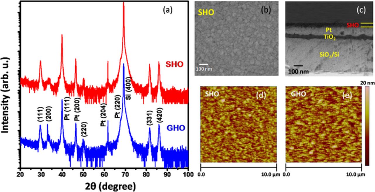
Figure 1. (a) XRD patterns of SHO and GHO films on platinum. Both the films show nearly the same diffractograms with a definite cubic phase without any evidence of monoclinic or orthorhombic phases. (b) SEM micrograph and (c) cross-sectional SEM image of SHO film, (d-e) represent the AFM-topography map of SHO and GHO, respectively.
The evolution of P-V hysteresis loops in Pt/SHO/Pt and Pt/GHO/Pt capacitors under different DC voltage sweep cycles of ± 4 V at 20 kHz is represented in Fig. 2a. It can be observed that the cyclic voltage sweep gives rise to an enhancement in ferroelectric response in both the films. As evident form Figs. 2a and 2b, at an initial DC voltage sweep with a maximum voltage of 4 V, no actual ferroelectric hysteresis was observed even up to 150 voltage sweep cycles. After 150 cycles at the same conditions, a hysteresis loop starts to emerge and become distinct after 400 continuous cycles. Also, ferroelectric hysteresis was observed with enhanced remnant polarization and coercive field depending on the increase in number of DC sweep cycles. The maximum values of remnant polarization [(Pr)max = (Pr + + Pr −)/2] ∼13.5 and 12 μC/cm2, and coercive field [(Ec)max = (Ec + + Ec −)/2] ∼334 and 384 kV/cm were observed after 600 cycles in SHO and GHO thin films, respectively, which exhibit the improved ferroelectric behavior in our thin films as compare to the previously reported Gd-doped HfO2 thin films deposited by atomic layer deposition (ALD) technique with same doping concentration of Gd.8 We observed that a definite amount of wake-up cycles is required to enhance the hysteresis and Pr as well as EC in these films. Our results were found to be in agreement with the previously published reports by Zhou et al.13 in ALD deposited Si-doped HfO2 thin films and later on by Starschich et al.11 in chemical solution deposited Y-doped HfO2 thin films, where the “wake-up” effect in the polarization hysteresis was observed. The “wake-up” (de-aging) effect corresponds to an increase in the remnant polarization caused by the application of subsequent bipolar voltage cycles. We can expect presence of the charged defects (mainly oxygen vacancies) in our doped- HfO2 thin films due to the relatively low oxygen partial pressure (∼0.5 Pa) used during film deposition.17 These charged defects near the electrode/ferroelectric interface inhibit the growth of domains of opposite polarity.13 High interfacial charged defects can lead to the band banding with the formation of a depletion layer where the built-in electric field (Ebi) across the depletion region can be expected to result in local alignment of ferroelectric dipoles.2 Further, successive bipolar voltage cycles can cause removal or redistribution of these charged defects, which reduces the Ebi by de-pinning more and more domains to participate in polarization switching. This increase in polarization switching leads to enhanced remnant polarization. In addition, non-linear small signal capacitance-voltage responses from Pt/SHO/Pt and Pt/GHO/Pt capacitors showed the ferroelectric behavior where the double peaks in the relative permittivity (calculated from the measured capacitance) versus voltage curves were observed near the vicinity of the coercive voltages while sweeping a full hysteresis loop in the same voltage range ± 4 V, as depicted in Figs. 2c and 2d. The observation of characteristics maxima (double peaks) in the voltage dependent relative permittivity (ɛr) is a characteristic property of ferroelectric capacitors and can be explained in terms of increased domain walls movement at the coercive fields.18 At the coercive field, the maximum number of domain walls exists in the ferroelectric, which can contribute to the permittivity through its reversible motion giving rise to the maxima in permittivity versus voltage curve.18 Thus, the domain wall motions give the largest contribution to the permittivity in ferroelectrics. Additionally, the low dielectric constant (about 50) observed in these samples make them good candidates for metal-ferroelectric-insulator-semiconductor (MFIS) memory structures with good interface properties.
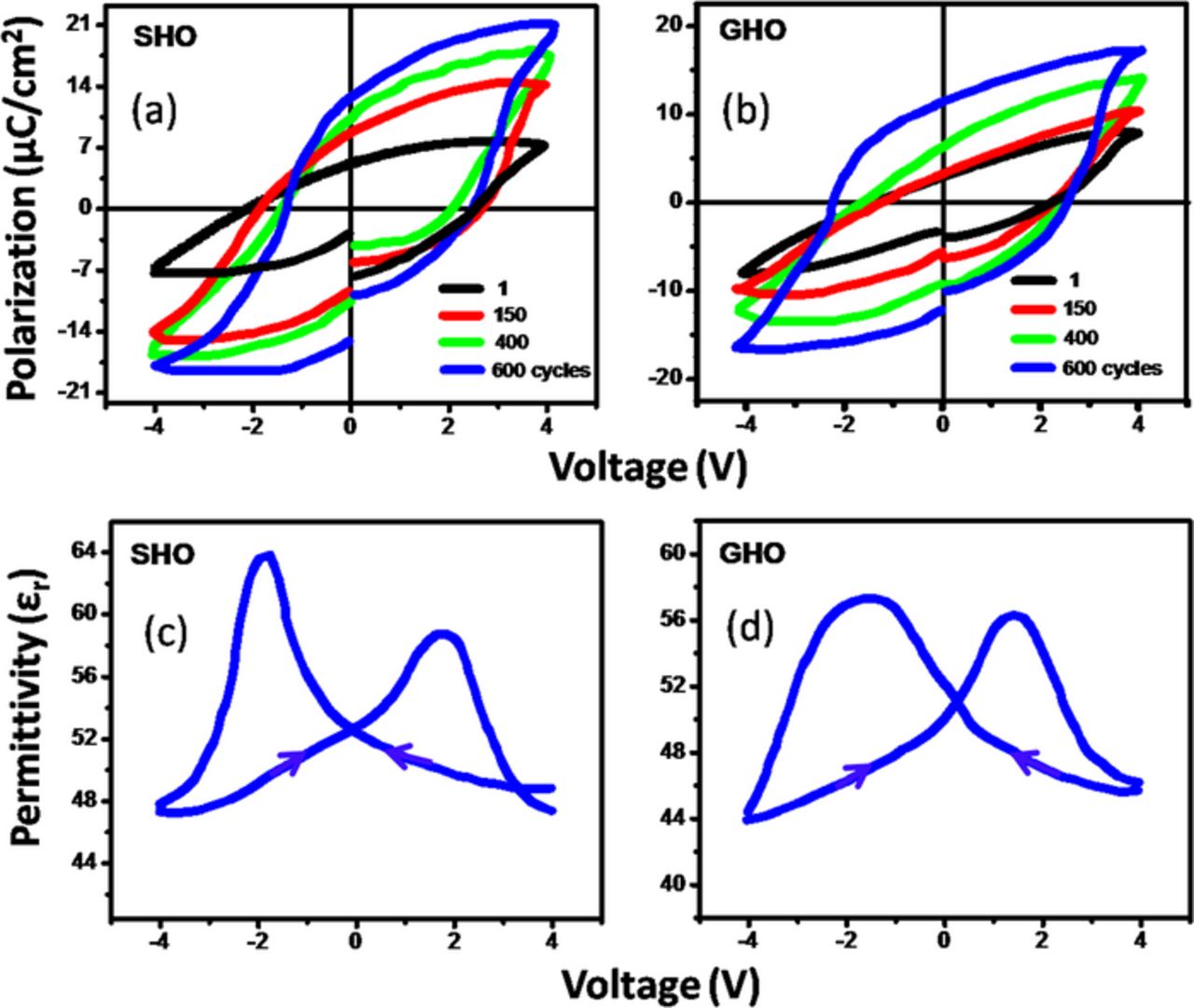
Figure 2. (a-b) Macroscopic ferroelectric hysteresis loops are established after a wake-up cycling period and (c-d) the characteristic ferroelectric capacitance peaks in dual sweep C-V for Pt/SHO/Pt and Pt/GHO/Pt capacitors, respectively.
To confirm the ferroelectric nature of these films, the local ferroelectric properties were also studied using PFM measurements. The out-of-plane piezoresponse hysteresis loops were measured as a function of applied voltage of ± 4 V on the same capacitors where all the P-V cyclic and capacitance measurements were performed. As shown in Figs. 3a–3d, the phase and amplitude hysteresis loops measured on Pt/SHO/Pt and Pt/GHO/Pt capacitors showed well-defined phase hysteresis (with the phase change of ∼ 180°) and butterfly shaped amplitude loops revealing that both of the films possess ferroelectric character at the nanoscale level.
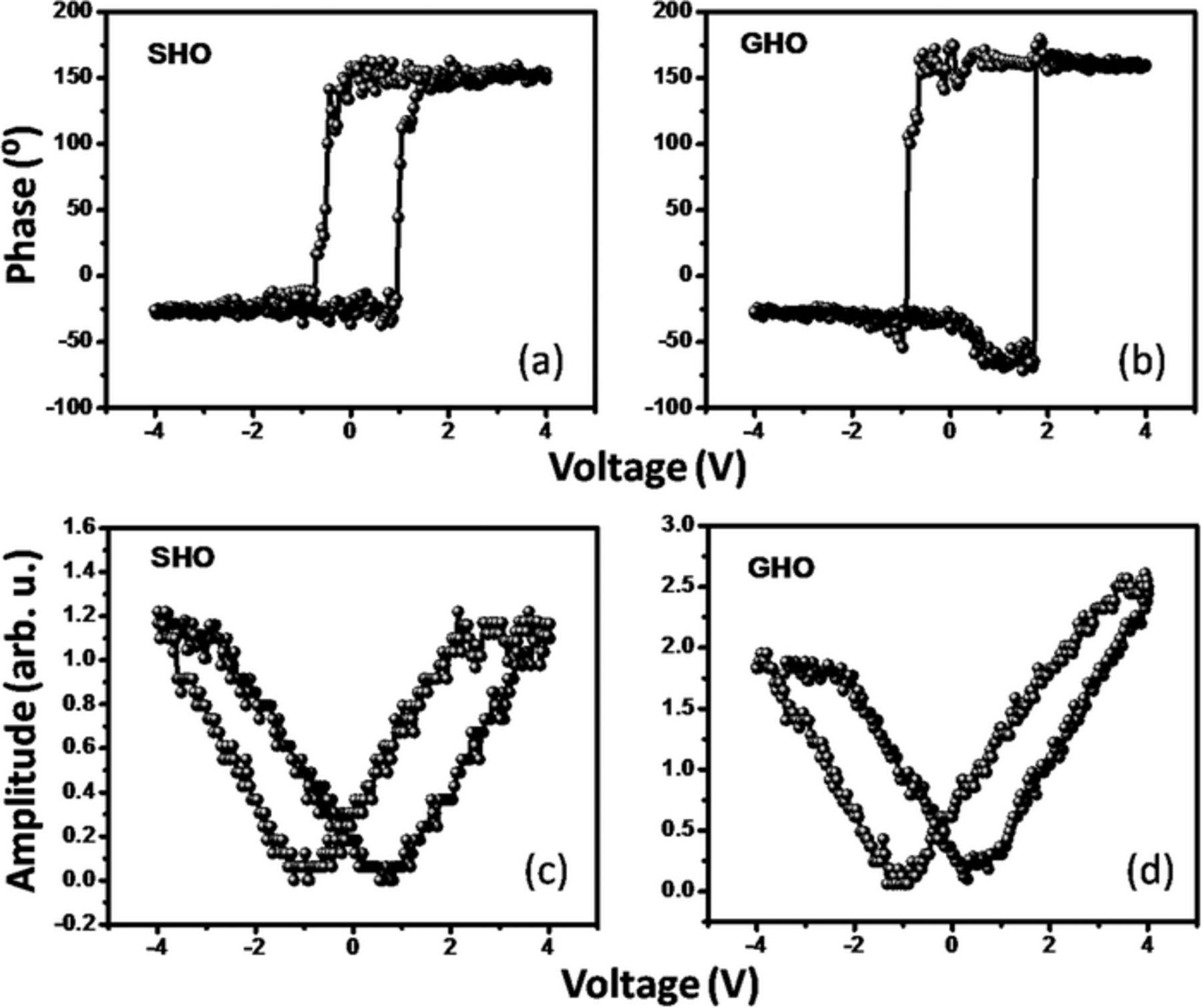
Figure 3. Piezoresponse force microscopy (PFM) measurements show: (a-b) phase and (c-d) amplitude hysteresis loops measured on SHO/Pt and GHO/Pt structures.
Conclusions
In summary, we have demonstrated the ferroelectric nature of Sm or Gd-doped HfO2 thin films deposited by SPLD technique. The macroscopic ferroelectric measurements revealed maximum remanent polarization of ∼13.5 (∼12) μC/cm2 and coercive field of ∼334 (∼384) kV/cm in 60 nm thick SHO (GHO) thin film. Piezoforce macroscopic measurements in terms of phase hysteresis and butterfly amplitude loops further confirmed the ferroelectric nature of SHO and GHO films. It was observed that wake-up cycles are essential to get polarization hysteresis and to enhance the remnant polarization. Our ferroelectric thin films can have promising potentials for future lead free ferroelectric non-volatile memory.
Acknowledgment
Financial support from DOE grant No. DE-FG02-08ER46526 is acknowledged. Y. S., D. B., and R. A. are grateful to IFN for graduate fellowship and S. P. P. is thankful to IFN for post-doctoral fellowship under NSF grant # 1002410.